153
Контроль
умения говорить.
Подготовьте
и сделайте сообщения по следующим
темам:
Film
technology and semiconductor technology
Silicon
for microelectronics.
Oxidation
and its function.
The
techniques for the deposition of thin films. Текст
3.10
С
Прочитайте
текст. Изложите свои выводы о преимуществах
приборов на арсениде галлия. Используя
рисунок, опишите принцин действия
прибора. На основе прочитанного и
ваших знаний но специальности подготовьте
сообщения о: а) технологии
полупроводниковых приборов и ИС; б)
новых материалах и новой технологии
производства ИС, БИС и СБИС. Ill—V
Semiconductor
Integrated Circuits
III—V
semiconductors
attract the attention of scientists and manufacturers working
in the field of microelectronics. This interest is based upon the
ability of these materials to satisfy a wide variety of needs.
Technological
applications include high speed processing, communications,
sensing and imagining, and many others. Integrated circuits with
various combinations of MESFET, JFET, bipolar, Gunn, Schottky diode,
laser diode, optical detector, light guide, acoustic wave, and other
assorted functions are being explored, developed and utilized.
One
of the first large-scale applications of III—V semiconductors
was light-emitting diodes (LEDs) which are two terminal devices
that emit light when a forward-bias current is passed through a p-
n
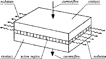
junction. An energy state and device construction is given in Fig.
3.
When
an electron in the conduction band combines with a hole in the
valence band, the energy is emitted as a photon and light is
Produced. Of course, non-radiative combination processes and light
re-absorption
must be minimized for high efficiency. To emit light yisible
to the human eye, a band gap near 2 e V is necessary to pro- vide
the proper photon energy, which produces red-green light.Раздел 3 Третье занятие
154
Микроэлектроника
настоящее и будущее
Fig.3
At
the beginning of the 1970’s, the GaAs MESFET device was developed
for use in circuits such as microwave amplifiers operating in the
frequencies range from about 2 to 12 Ghz. The device is fabricated
on a base of single-crystal semi-insulating GaAs. A GaAs film
containing a closely-controlled concentration of я-type
dopant atoms is epitaxially deposited on the GaAs wafer. The devices
are completed by etching “mesas” or islands to electrically
isolate the device and by adding low resistance contacts and a
gate electrode. The gate length is typically 1 mm.
The
first integration of GaAs M ESFET transistors into logic gates was
done in 1974. These gates have been integrated into gated flip-flop
integrated circuits and used for prescalers and time-interval
measurements. These GaAs integrated circuits operate at
substantially higher speeds than silicon ICs because of a
combination of higher transcon- ductance due to higher substrate
resistivity. The higher substrate resistivity in GaAs is a
result of its larger bandgap. Semi-insulating GaAs
material
naturally provides device-to-device electrical isolation.
Digital
capability in GaAs has passed from the SSI (small-scale
integration,
- 10 gates) realm into the MSI (medium-scale integra- tion, ~ 100
gates), and is headed for LSI (large-scale integration, ~ 1000
gates). Fabrication of an 8 x 8 bit parallel multiplier (1008 gates
fabri- cated from approximately 6000 transistors and diodes) has
been re'