- •Verilog-AMS
- •Language Reference Manual
- •Table of Contents
- •1. Verilog-AMS introduction
- •1.1 Overview
- •1.2 Mixed-signal language features
- •1.3 Systems
- •1.3.1 Conservative systems
- •1.3.1.1 Reference nodes
- •1.3.1.2 Reference directions
- •1.3.2 Kirchhoff’s Laws
- •1.3.3 Natures, disciplines, and nets
- •1.3.4 Signal-flow systems
- •1.3.5 Mixed conservative/signal flow systems
- •1.4 Conventions used in this document
- •1.5 Contents
- •2. Lexical conventions
- •2.1 Overview
- •2.2 Lexical tokens
- •2.3 White space
- •2.4 Comments
- •2.5 Operators
- •2.6 Numbers
- •2.6.1 Integer constants
- •2.6.2 Real constants
- •2.7 String literals
- •2.8 Identifiers, keywords, and system names
- •2.8.1 Escaped identifiers
- •2.8.2 Keywords
- •2.8.3 System tasks and functions
- •2.8.4 Compiler directives
- •2.9 Attributes
- •2.9.1 Standard attributes
- •2.9.2 Syntax
- •3. Data types
- •3.1 Overview
- •3.2 Integer and real data types
- •3.2.1 Output variables
- •3.3 String data type
- •3.4 Parameters
- •3.4.1 Type specification
- •3.4.2 Value range specification
- •3.4.3 Parameter units and descriptions
- •3.4.4 Parameter arrays
- •3.4.5 Local parameters
- •3.4.6 String parameters
- •3.4.7 Parameter aliases
- •3.5 Genvars
- •3.6 Net_discipline
- •3.6.1 Natures
- •3.6.1.1 Derived natures
- •3.6.1.2 Attributes
- •3.6.1.3 User-defined attributes
- •3.6.2 Disciplines
- •3.6.2.1 Nature binding
- •3.6.2.2 Domain binding
- •3.6.2.3 Empty disciplines
- •3.6.2.4 Discipline of nets and undeclared nets
- •3.6.2.5 Overriding nature attributes from discipline
- •3.6.2.6 Deriving natures from disciplines
- •3.6.2.7 User-defined attributes
- •3.6.3 Net discipline declaration
- •3.6.3.1 Net descriptions
- •3.6.3.2 Net Discipline Initial (Nodeset) Values
- •3.6.4 Ground declaration
- •3.6.5 Implicit nets
- •3.7 Real net declarations
- •3.8 Default discipline
- •3.9 Disciplines of primitives
- •3.10 Discipline precedence
- •3.11 Net compatibility
- •3.11.1 Discipline and Nature Compatibility
- •3.12 Branches
- •3.13 Namespace
- •3.13.1 Nature and discipline
- •3.13.2 Access functions
- •3.13.4 Branch
- •4. Expressions
- •4.1 Overview
- •4.2 Operators
- •4.2.1 Operators with real operands
- •4.2.1.1 Real to integer conversion
- •4.2.1.2 Integer to real conversion
- •4.2.1.3 Arithmetic conversion
- •4.2.2 Operator precedence
- •4.2.3 Expression evaluation order
- •4.2.4 Arithmetic operators
- •4.2.5 Relational operators
- •4.2.6 Case equality operators
- •4.2.7 Logical equality operators
- •4.2.8 Logical operators
- •4.2.9 Bitwise operators
- •4.2.10 Reduction operators
- •4.2.11 Shift operators
- •4.2.12 Conditional operator
- •4.2.13 Concatenations
- •4.3 Built-in mathematical functions
- •4.3.1 Standard mathematical functions
- •4.3.2 Transcendental functions
- •4.4 Signal access functions
- •4.5 Analog operators
- •4.5.1 Vector or array arguments to analog operators
- •4.5.2 Analog operators and equations
- •4.5.3 Time derivative operator
- •4.5.4 Time integral operator
- •4.5.5 Circular integrator operator
- •4.5.6 Derivative operator
- •4.5.7 Absolute delay operator
- •4.5.8 Transition filter
- •4.5.9 Slew filter
- •4.5.10 last_crossing function
- •4.5.11 Laplace transform filters
- •4.5.11.1 laplace_zp
- •4.5.11.2 laplace_zd
- •4.5.11.3 laplace_np
- •4.5.11.4 laplace_nd
- •4.5.11.5 Examples
- •4.5.12 Z-transform filters
- •4.5.13 Limited exponential
- •4.5.14 Constant versus dynamic arguments
- •4.5.15 Restrictions on analog operators
- •4.6 Analysis dependent functions
- •4.6.1 Analysis
- •4.6.2 DC analysis
- •4.6.3 AC stimulus
- •4.6.4 Noise
- •4.6.4.1 white_noise
- •4.6.4.2 flicker_noise
- •4.6.4.3 noise_table
- •4.6.4.4 Noise model for diode
- •4.6.4.5 Correlated noise
- •4.7 User defined functions
- •4.7.1 Defining an analog user defined function
- •4.7.2 Returning a value from an analog user defined function
- •4.7.2.1 Analog user defined function identifier variable
- •4.7.2.2 Output arguments
- •4.7.2.3 Inout arguments
- •4.7.3 Calling an analog user defined function
- •5. Analog behavior
- •5.1 Overview
- •5.2 Analog procedural block
- •5.2.1 Analog initial block
- •5.3 Block statements
- •5.3.1 Sequential blocks
- •5.3.2 Block names
- •5.4 Analog signals
- •5.4.1 Access functions
- •5.4.2 Probes and sources
- •5.4.2.1 Probes
- •5.4.2.2 Sources
- •5.4.3 Port branches
- •5.4.4 Unassigned sources
- •5.5 Accessing net and branch signals and attributes
- •5.5.1 Accessing net and branch signals
- •5.5.2 Signal access for vector branches
- •5.5.3 Accessing attributes
- •5.6 Contribution statements
- •5.6.1 Direct branch contribution statements
- •5.6.1.1 Relations
- •5.6.1.2 Evaluation
- •5.6.1.3 Value retention
- •5.6.2 Examples
- •5.6.2.1 The four controlled sources
- •5.6.3 Resistor and conductor
- •5.6.4 RLC circuits
- •5.6.5 Switch branches
- •5.6.6 Implicit Contributions
- •5.6.7 Indirect branch contribution statements
- •5.6.7.1 Multiple indirect contributions
- •5.6.7.2 Indirect and direct contribution
- •5.7 Analog procedural assignments
- •5.8 Analog conditional statements
- •5.8.1 if-else-if statement
- •5.8.2 Examples
- •5.8.3 Case statement
- •5.8.4 Restrictions on conditional statements
- •5.9 Looping statements
- •5.9.1 Repeat and while statements
- •5.9.2 For statements
- •5.9.3 Analog For Statements
- •5.10 Analog event control statements
- •5.10.1 Event OR operator
- •5.10.2 Global events
- •5.10.3 Monitored events
- •5.10.3.1 cross function
- •5.10.3.2 above function
- •5.10.3.3 timer function
- •5.10.4 Named events
- •5.10.5 Digital events in analog behavior
- •6. Hierarchical structures
- •6.1 Overview
- •6.2 Modules
- •6.2.1 Top-level modules
- •6.2.2 Module instantiation
- •6.3 Overriding module parameter values
- •6.3.1 Defparam statement
- •6.3.2 Module instance parameter value assignment by order
- •6.3.3 Module instance parameter value assignment by name
- •6.3.4 Parameter dependence
- •6.3.5 Detecting parameter overrides
- •6.3.6 Hierarchical system parameters
- •6.4 Paramsets
- •6.4.1 Paramset statements
- •6.4.2 Paramset overloading
- •6.4.3 Paramset output variables
- •6.5 Ports
- •6.5.1 Port definition
- •6.5.2 Port declarations
- •6.5.2.1 Port type
- •6.5.2.2 Port direction
- •6.5.3 Real valued ports
- •6.5.4 Connecting module ports by ordered list
- •6.5.5 Connecting module ports by name
- •6.5.6 Detecting port connections
- •6.5.7 Port connection rules
- •6.5.7.1 Matching size rule
- •6.5.7.2 Resolving discipline of undeclared interconnect signal
- •6.5.8 Inheriting port natures
- •6.6 Generate constructs
- •6.6.1 Loop generate constructs
- •6.6.2 Conditional generate constructs
- •6.6.2.1 Dynamic parameters
- •6.6.3 External names for unnamed generate blocks
- •6.7 Hierarchical names
- •6.7.1 Usage of hierarchical references
- •6.8 Scope rules
- •6.9 Elaboration
- •6.9.1 Concatenation of analog blocks
- •6.9.2 Elaboration and paramsets
- •6.9.3 Elaboration and connectmodules
- •6.9.4 Order of elaboration
- •7. Mixed signal
- •7.1 Overview
- •7.2 Fundamentals
- •7.2.1 Domains
- •7.2.2 Contexts
- •7.2.3 Nets, nodes, ports, and signals
- •7.2.4 Mixed-signal and net disciplines
- •7.3 Behavioral interaction
- •7.3.1 Accessing discrete nets and variables from a continuous context
- •7.3.2 Accessing X and Z bits of a discrete net in a continuous context
- •7.3.2.1 Special floating point values
- •7.3.3 Accessing continuous nets and variables from a discrete context
- •7.3.4 Detecting discrete events in a continuous context
- •7.3.5 Detecting continuous events in a discrete context
- •7.3.6 Concurrency
- •7.3.6.1 Analog event appearing in a digital event control
- •7.3.6.2 Digital event appearing in an analog event control
- •7.3.6.3 Analog primary appearing in a digital expression
- •7.3.6.4 Analog variables appearing in continuous assigns
- •7.3.6.5 Digital primary appearing in an analog expression
- •7.3.7 Function calls
- •7.4 Discipline resolution
- •7.4.1 Compatible discipline resolution
- •7.4.2 Connection of discrete-time disciplines
- •7.4.3 Connection of continuous-time disciplines
- •7.4.4 Resolution of mixed signals
- •7.4.4.1 Basic discipline resolution algorithm
- •7.4.4.2 Detail discipline resolution algorithm
- •7.4.4.3 Coercing discipline resolution
- •7.5 Connect modules
- •7.6 Connect module descriptions
- •7.7 Connect specification statements
- •7.7.1 Connect module auto-insertion statement
- •7.7.2 Discipline resolution connect statement
- •7.7.2.1 Connect Rule Resolution Mechanism
- •7.7.3 Parameter passing attribute
- •7.7.4 connect_mode
- •7.8 Automatic insertion of connect modules
- •7.8.1 Connect module selection
- •7.8.2 Signal segmentation
- •7.8.3 connect_mode parameter
- •7.8.3.1 merged
- •7.8.3.2 split
- •7.8.4 Rules for driver-receiver segregation and connect module selection and insertion
- •7.8.5 Instance names for auto-inserted instances
- •7.8.5.1 Port names for Verilog built-in primitives
- •8. Scheduling semantics
- •8.1 Overview
- •8.2 Analog simulation cycle
- •8.2.1 Nodal analysis
- •8.2.2 Transient analysis
- •8.2.3 Convergence
- •8.3 Mixed-signal simulation cycle
- •8.3.1 Circuit initialization
- •8.3.2 Mixed-signal DC analysis
- •8.3.3 Mixed-signal transient analysis
- •8.3.3.1 Concurrency
- •8.3.3.2 Analog macro process scheduling semantics
- •8.3.3.3 A/D boundary timing
- •8.3.4 The synchronization loop
- •8.3.5 Synchronization and communication algorithm
- •8.3.6 Assumptions about the analog and digital algorithms
- •8.4 Scheduling semantics for the digital engine
- •8.4.1 The stratified event queue
- •8.4.2 The Verilog-AMS digital engine reference model
- •8.4.3 Scheduling implication of assignments
- •8.4.3.1 Continuous assignment
- •8.4.3.2 Procedural continuous assignment
- •8.4.3.3 Blocking assignment
- •8.4.3.4 Non blocking assignment
- •8.4.3.5 Switch (transistor) processing
- •8.4.3.6 Processing explicit D2A events (region 1b)
- •8.4.3.7 Processing analog macro-process events (region 3b)
- •9. System tasks and functions
- •9.1 Overview
- •9.2 Categories of system tasks and functions
- •9.3 System tasks/functions executing in the context of the Analog Simulation Cycle
- •9.4 Display system tasks
- •9.4.1 Behavior of the display tasks in the analog context
- •9.4.2 Escape sequences for special characters
- •9.4.3 Format specifications
- •9.4.4 Hierarchical name format
- •9.4.5 String format
- •9.4.6 Behavior of the display tasks in the analog block during iterative solving
- •9.4.7 Extensions to the display tasks in the digital context
- •9.5.1 Opening and closing files
- •9.5.1.1 opening and closing files during multiple analyses
- •9.5.1.2 Sharing of file descriptors between the analog and digital contexts
- •9.5.2 File output system tasks
- •9.5.3 Formatting data to a string
- •9.5.4 Reading data from a file
- •9.5.4.1 Reading a line at a time
- •9.5.4.2 Reading formatted data
- •9.5.5 File positioning
- •9.5.6 Flushing output
- •9.5.7 I/O error status
- •9.5.8 Detecting EOF
- •9.5.9 Behavior of the file I/O tasks in the analog block during iterative solving
- •9.6 Timescale system tasks
- •9.7 Simulation control system tasks
- •9.7.1 $finish
- •9.7.2 $stop
- •9.7.3 $fatal, $error, $warning, and $info
- •9.8 PLA modeling system tasks
- •9.9 Stochastic analysis system tasks
- •9.10 Simulator time system functions
- •9.11 Conversion system functions
- •9.12 Command line input
- •9.13 Probabilistic distribution system functions
- •9.13.1 $random and $arandom
- •9.13.2 distribution functions
- •9.13.3 Algorithm for probablistic distribution
- •9.14 Math system functions
- •9.15 Analog kernel parameter system functions
- •9.16 Dynamic simulation probe function
- •9.17 Analog kernel control system tasks and functions
- •9.17.1 $discontinuity
- •9.17.2 $bound_step task
- •9.17.3 $limit
- •9.18 Hierarchical parameter system functions
- •9.19 Explicit binding detection system functions
- •9.20 Table based interpolation and lookup system function
- •9.20.1 Table data source
- •9.20.2 Control string
- •9.20.3 Example control strings
- •9.20.4 Lookup algorithm
- •9.20.5 Interpolation algorithms
- •9.20.6 Example
- •9.21 Connectmodule driver access system functions and operator
- •9.21.1 $driver_count
- •9.21.2 $driver_state
- •9.21.3 $driver_strength
- •9.21.4 driver_update
- •9.21.5 Receiver net resolution
- •9.21.6 Connect module example using driver access functions
- •9.22 Supplementary connectmodule driver access system functions
- •9.22.1 $driver_delay
- •9.22.2 $driver_next_state
- •9.22.3 $driver_next_strength
- •9.22.4 $driver_type
- •10. Compiler directives
- •10.1 Overview
- •10.2 `default_discipline
- •10.3 `default_transition
- •10.4 `define and `undef
- •10.5 Predefined macros
- •10.6 `begin_keywords and `end_keywords
- •11. Using VPI routines
- •11.1 Overview
- •11.2 The VPI interface
- •11.2.1 VPI callbacks
- •11.2.2 VPI access to Verilog-AMS HDL objects and simulation objects
- •11.2.3 Error handling
- •11.3 VPI object classifications
- •11.3.1 Accessing object relationships and properties
- •11.3.2 Delays and values
- •11.4 List of VPI routines by functional category
- •11.5 Key to object model diagrams
- •11.5.1 Diagram key for objects and classes
- •11.5.2 Diagram key for accessing properties
- •11.5.3 Diagram key for traversing relationships
- •11.6 Object data model diagrams
- •11.6.1 Module
- •11.6.2 Nature, discipline
- •11.6.3 Scope, task, function, IO declaration
- •11.6.4 Ports
- •11.6.5 Nodes
- •11.6.6 Branches
- •11.6.7 Quantities
- •11.6.8 Nets
- •11.6.9 Regs
- •11.6.10 Variables, named event
- •11.6.11 Memory
- •11.6.12 Parameter, specparam
- •11.6.13 Primitive, prim term
- •11.6.15 Module path, timing check, intermodule path
- •11.6.16 Task and function call
- •11.6.17 Continuous assignment
- •11.6.18 Simple expressions
- •11.6.19 Expressions
- •11.6.20 Contribs
- •11.6.21 Process, block, statement, event statement
- •11.6.22 Assignment, delay control, event control, repeat control
- •11.6.23 If, if-else, case
- •11.6.24 Assign statement, deassign, force, release, disable
- •11.6.25 Callback, time queue
- •12. VPI routine definitions
- •12.1 Overview
- •12.2 vpi_chk_error()
- •12.3 vpi_compare_objects()
- •12.4 vpi_free_object()
- •12.6 vpi_get_cb_info()
- •12.7 vpi_get_analog_delta()
- •12.8 vpi_get_analog_freq()
- •12.9 vpi_get_analog_time()
- •12.10 vpi_get_analog_value()
- •12.11 vpi_get_delays()
- •12.13 vpi_get_analog_systf_info()
- •12.14 vpi_get_systf_info()
- •12.15 vpi_get_time()
- •12.16 vpi_get_value()
- •12.17 vpi_get_vlog_info()
- •12.18 vpi_get_real()
- •12.19 vpi_handle()
- •12.20 vpi_handle_by_index()
- •12.21 vpi_handle_by_name()
- •12.22 vpi_handle_multi()
- •12.22.1 Derivatives for analog system task/functions
- •12.22.2 Examples
- •12.23 vpi_iterate()
- •12.24 vpi_mcd_close()
- •12.25 vpi_mcd_name()
- •12.26 vpi_mcd_open()
- •12.27 vpi_mcd_printf()
- •12.28 vpi_printf()
- •12.29 vpi_put_delays()
- •12.30 vpi_put_value()
- •12.31 vpi_register_cb()
- •12.31.1 Simulation-event-related callbacks
- •12.31.2 Simulation-time-related callbacks
- •12.31.3 Simulator analog and related callbacks
- •12.31.4 Simulator action and feature related callbacks
- •12.32 vpi_register_analog_systf()
- •12.32.1 System task and function callbacks
- •12.32.2 Declaring derivatives for analog system task/functions
- •12.32.3 Examples
- •12.33 vpi_register_systf()
- •12.33.1 System task and function callbacks
- •12.33.2 Initializing VPI system task/function callbacks
- •12.34 vpi_remove_cb()
- •12.35 vpi_scan()
- •12.36 vpi_sim_control()
- •A.1 Source text
- •A.1.1 Library source text
- •A.1.2 Verilog source text
- •A.1.3 Module parameters and ports
- •A.1.4 Module items
- •A.1.5 Configuration source text
- •A.1.6 Nature Declaration
- •A.1.7 Discipline Declaration
- •A.1.8 Connectrules Declaration
- •A.1.9 Paramset Declaration
- •A.2 Declarations
- •A.2.1 Declaration types
- •A.2.1.1 Module parameter declarations
- •A.2.1.2 Port declarations
- •A.2.1.3 Type declarations
- •A.2.2 Declaration data types
- •A.2.2.1 Net and variable types
- •A.2.2.2 Strengths
- •A.2.2.3 Delays
- •A.2.3 Declaration lists
- •A.2.4 Declaration assignments
- •A.2.5 Declaration ranges
- •A.2.6 Function declarations
- •A.2.7 Task declarations
- •A.2.8 Block item declarations
- •A.3 Primitive instances
- •A.3.1 Primitive instantiation and instances
- •A.3.2 Primitive strengths
- •A.3.3 Primitive terminals
- •A.3.4 Primitive gate and switch types
- •A.4 Module instantiation and generate construct
- •A.4.1 Module instantiation
- •A.4.2 Generate construct
- •A.5 UDP declaration and instantiation
- •A.5.1 UDP declaration
- •A.5.2 UDP ports
- •A.5.3 UDP body
- •A.5.4 UDP instantiation
- •A.6 Behavioral statements
- •A.6.1 Continuous assignment statements
- •A.6.2 Procedural blocks and assignments
- •A.6.3 Parallel and sequential blocks
- •A.6.4 Statements
- •A.6.5 Timing control statements
- •A.6.6 Conditional statements
- •A.6.7 Case statements
- •A.6.8 Looping statements
- •A.6.9 Task enable statements
- •A.6.10 Contribution statements
- •A.7 Specify section
- •A.7.1 Specify block declaration
- •A.7.2 Specify path declarations
- •A.7.3 Specify block terminals
- •A.7.4 Specify path delays
- •A.7.5 System timing checks
- •A.7.5.1 System timing check commands
- •A.7.5.2 System timing check command arguments
- •A.7.5.3 System timing check event definitions
- •A.8 Expressions
- •A.8.1 Concatenations
- •A.8.2 Function calls
- •A.8.3 Expressions
- •A.8.4 Primaries
- •A.8.5 Expression left-side values
- •A.8.6 Operators
- •A.8.7 Numbers
- •A.8.8 Strings
- •A.8.9 Analog references
- •A.9 General
- •A.9.1 Attributes
- •A.9.2 Comments
- •A.9.3 Identifiers
- •A.9.4 White space
- •A.10 Details
- •C.1 Verilog-AMS introduction
- •C.1.1 Verilog-A overview
- •C.1.2 Verilog-A language features
- •C.2 Lexical conventions
- •C.3 Data types
- •C.4 Expressions
- •C.5 Analog signals
- •C.6 Analog behavior
- •C.7 Hierarchical structures
- •C.8 Mixed signal
- •C.9 Scheduling semantics
- •C.10 System tasks and functions
- •C.11 Compiler directives
- •C.12 Using VPI routines
- •C.13 VPI routine definitions
- •C.14 Analog language subset
- •C.15 List of keywords
- •C.16 Standard definitions
- •C.17 SPICE compatibility
- •C.18 Changes from previous Verilog-A LRM versions
- •C.19 Obsolete functionality
- •D.1 The disciplines.vams file
- •D.2 The constants.vams file
- •D.3 The driver_access.vams file
- •E.1 Introduction
- •E.1.1 Scope of compatibility
- •E.1.2 Degree of incompatibility
- •E.2 Accessing Spice objects from Verilog-AMS HDL
- •E.2.1 Case sensitivity
- •E.2.2 Examples
- •E.3 Accessing Spice models
- •E.3.1 Accessing Spice subcircuits
- •E.3.1.1 Accessing Spice primitives
- •E.4 Preferred primitive, parameter, and port names
- •E.4.1 Unsupported primitives
- •E.4.2 Discipline of primitives
- •E.4.2.1 Setting the discipline of analog primitives
- •E.4.2.2 Resolving the disciplines of analog primitives
- •E.4.3 Name scoping of SPICE primitives
- •E.4.4 Limiting algorithms
- •E.5 Other issues
- •E.5.1 Multiplicity factor on subcircuits
- •E.5.2 Binning and libraries
- •F.1 Discipline resolution
- •F.2 Resolution of mixed signals
- •F.2.1 Default discipline resolution algorithm
- •F.2.2 Alternate expanded analog discipline resolution algorithm
- •G.1 Changes from previous LRM versions
- •G.2 Obsolete functionality
- •G.2.1 Forever
- •G.2.2 NULL
- •G.2.3 Generate
- •G.2.4 `default_function_type_analog
|
Accellera |
Analog and Mixed-signal Extensions to Verilog HDL |
Version 2.3.1, June 1, 2009 |
8.3.2 Mixed-signal DC analysis
Mixed-signal DC analysis is the process of finding the steady state of the circuit, which is the DC operating point for transient and AC analysis. The steady state of the digital circuit is defined as the final state at time 0 when all analog and digital events are executed. For mixed-signal DC analysis, the processes of the analog DC analysis and the digital simulation at time 0 are executed iteratively, starting with the initialization phase (including analog and digital) defined in circuit initialization (8.3.1), until all signals at the A/D boundaries reach steady state. The signal propagation at the A/D boundaries follows the same scheduling semantics as are defined in transient analysis in the following sections.
8.3.3 Mixed-signal transient analysis
A Verilog-AMS simulation consists of a number of analog and digital processes communicating via events, shared memory and conservative nodes. Analog processes that share conservative nodes are “solved” jointly and can be viewed as a “macro” process, there may be any number “macro” processes, and it is left up to the implementation whether it solves them in a single matrix, multiple matrices or uses other techniques but it should abide by the accuracy stipulated in the disciplines and analog functions.
8.3.3.1 Concurrency
Most (current) simulators are single-threaded in execution, meaning that although the semantics of VerilogAMS imply processes are active concurrently, the reality is that they are not. If an implementation is genuinely multi-threaded, it should not evaluate processes that directly share memory concurrently, as there are no data locking semantics in Verilog-AMS.
8.3.3.2 Analog macro process scheduling semantics
The internal evaluation of an analog macro process is described in 8.2.2. Once the analog engine has determined its behavior for a given time, it must communicate the results to other processes in the mixed signal simulation through events and shared variables. When an analog macro process is evaluated, the analog engine finds a potential “solution” at a future time (the “acceptance time”), and it stores (but does not communicate) values1 for all the process’s nodes up to that time. A “wake up” event is scheduled for the acceptance time of the process, and the process is then inactive until it is either woken up or receives an event from another process. If it is woken up by its own “wake up” event, it calculates a new solution point, acceptance time (and so forth) and deactivates. If it is woken up prior to acceptance time by an event that disturbs its current solution, it will cancel its own “wake up” event, accept at the wake-up time, recalculate its solution and schedule a new “wake up” event for the new acceptance time. The process may also wake itself up early for reevaluation by use of a timer (which can be viewed as just another process).
If the analog process identifies future analog events such as “crossings” or timer events (see 5.10.3) then it will schedule its wake-up event for the time of the first such event rather than the acceptance time. If the analog process is woken by such an analog event it will communicate any related events at that time and deactivate, rescheduling its wake-up for the next analog event or acceptance. Events to external processes generated from analog events are not communicated until the global simulation time reaches the time of the analog event.
If the time to acceptance is infinite then no wake-up event needs to be scheduled2.
Analog processes are sensitive to changes in all variables and digital signals read by the process unless that access is only in statements ‘guarded’ by event expressions. For example the following code implements a simple digital to analog convertor:
1Or derivatives w.r.t. time used to calculate the values. 2The case when all derivatives are zero - the circuit is stable.
181 |
Copyright © 2009 Accellera Organization, Inc. All rights reserved. |
Accellera |
|
Version 2.3.1, June 1, 2009 |
VERILOG-AMS |
module d2a(val,vo); // 16 bit D->A
parameter |
Vgain = 1.0/65536; |
input |
val; |
wire [15:0] val; |
|
electrical |
vo; |
analog begin
V(vo) <+ Vgain * val; end
endmodule
The output voltage V(vo) is reevaluated when any bit in val changes, which is not a problem if all the bits change simultaneously and no ‘X’ values occur. A practical design would require that the digital value is latched to avoid bad bit sequences, as in the following version:
module d2aC(clk,val,vo); // Clocked 16 bit D2A
parameter |
Vgain = 1.0/65536; |
input |
clk; |
input |
val; |
wire [15:0] val; |
|
electrical |
vo; |
real |
v_clkd; |
analog begin
@(posedge clk) v_clkd = Vgain * val; V(vo) <+ v_clkd;
end endmodule
Since val is now guarded by the @(posedge clock) expression the analog block is not sensitive to changes in val and only reevaluates when clk changes.
Macro processes can be evaluated separately but may be evaluated together1, in which case, the wake up event for one process will cause the re-evaluation of all or some of the processes. Users should bear this in mind when writing mixed-signal code, as it will mean that the code should be able to handle re-evaluation at any time (not just at its own event times).
8.3.3.3 A/D boundary timing
In the analog kernel, time is a floating point value. In the digital kernel time is an integer value. Hence, A2D events generally do not occur exactly at digital integer clock ticks.
For the purpose of reporting results and scheduling delayed future events, the digital kernel converts analog event times to digital times such that the error is limited to half the precison base for the module where the conversion occurs. For the examples below the timescale is 1ns/1ns, so the maximum scheduling error when swapping a digital module for its analog counterpart will be 0.5ns.
Consequently an A2D event that results in a D2A event being scheduled with zero (0) delay, shall have its effect propagated back to the analog kernel with zero (0) delay.
1This is implementation-dependent.
Copyright © 2009 Accellera Organization, Inc. |
182 |
|
Accellera |
Analog and Mixed-signal Extensions to Verilog HDL |
Version 2.3.1, June 1, 2009 |
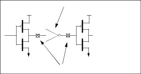
Zero delay inverter: always @(A) B<= !A;
A B
Connection modules
Figure 8-2: A zero delay inverter
If the circuit shown in Figure 8-2 is being simulated with a digital time resolution of 1e-9 (one (1) nanosecond) then all digital events shall be reported by the digital kernel as having occurred at an integer multiple of 1e-9. The A2D and D2A modules inserted are a simple level detector and a voltage ramp generator:
connectmodule a2d(i,o); |
|
parameter vdd = 1.0; |
|
ddiscrete |
o; |
input |
i; |
output |
o; |
reg |
o; |
electrical |
i; |
always begin @(cross(V(i) - vdd/2,+1))o = 1; end always begin @(cross(V(i) - vdd/2,-1))o = 0; end
endmodule
connectmodule d2a(i, o);
parameter |
vdd = |
1.0; |
parameter |
slewrate = 2.0/1e9; // V/s |
|
input |
i; |
|
output |
o; |
|
electrical |
o; |
// queued value |
reg |
qd_val, |
|
real |
nw_val; |
// delay to event |
et; |
||
real start_delay; |
// .. to ramp start |
always @(driver_update i) begin
nw_val = $driver_next_state(i,0); // assume one driver if (nw_val == qd_val) begin
// no change (assume delay constant) end else begin
et |
= $driver_delay(i,0) * 1e-9; // real delay |
qd_val |
= nw_val; |
end |
|
end |
|
analog begin |
start_delay = et - (vdd/2)/slewrate; |
@(qd_val) |
V(o) <+ vdd * transition(qd_val,start_delay,vdd/slewrate); end
endmodule
183 |
Copyright © 2009 Accellera Organization, Inc. All rights reserved. |
Accellera |
|
Version 2.3.1, June 1, 2009 |
VERILOG-AMS |
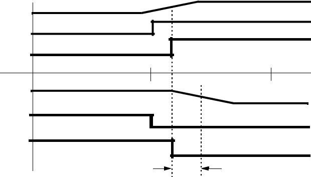
If connector A detects a positive threshold crossing, the resulting falling edge at connector B generated by the propagation of the signal through verilog inverter model shall be reported to the analog kernel with no further advance of analog time. The digital kernel will treat these events as if they occurred at the nearest nanosecond.
Example:
If A detects a positive crossing as a result of a transient solution at time 5.2e-9, the digital kernel shall report a rising edge at A at time 5.0e-9 and falling edge at B at time 5.0e-9, but the analog kernel shall see the transition at B begin at time 5.2e-9, as shown in Figure 8-3. D2As fed with zero delay events cannot be preemptive, so the crossover on the return is delayed from the digital event; zero-delay inverters are not physically realizable devices.
|
|
analog |
|
signal |
|
|
|
A |
|
digital reported |
|
|
|
|
|
|
|
digital real-time |
|
signal |
4 ns |
5 ns |
6 ns |
B |
|
analog |
|
|
|
|
|
|
|
digital reported |
|
|
|
digital real-time |
|
|
|
|
Analog gate delay |
Figure 8-3: Zero delay transient solution times
If the inverter equation is changed to use a one unit delay (always @(A) B<= #1 !A), then the timing is as in Figure 8-4.
Copyright © 2009 Accellera Organization, Inc. |
184 |