- •Contents
- •Preface
- •Related Documents
- •Typographic and Syntax Conventions
- •Introduction to the Virtuoso XL Layout Editor
- •Editing Your Technology File for Virtuoso XL Layout Editor
- •Sample Technology File
- •Virtuoso XL Technology File Requirements
- •Layer Rules
- •Devices
- •Physical Rules
- •Virtuoso XL Rules (lxRules)
- •Compactor Rules
- •Preparing Your Connectivity Source for the Virtuoso XL Layout Editor
- •Placing Design Elements
- •Using Design Variables
- •Netlist Processor Expressions
- •Analog Expression Language Expressions
- •Simulation Design Variables
- •Using One-to-Many Mapping
- •Iterated Instances and Bus Pins
- •Multiplication Factor (mfactor)
- •Series-Connection Factor (sfactor)
- •One-to-Many Assignment with the Update Device Correspondence
- •Using Many-to-Many or Many-to-One Mapping
- •Modifying Many-to-Many or Many-to-One Mapping Between Components
- •Deleting Many-to-Many or Many-to-One Mapping Between Components
- •Using Virtuoso XL Properties
- •Using the lxUseCell Property to Specify Layout Devices to Use
- •Using the lvsIgnore Property to Exclude Schematic Symbols
- •Using the lxlgnoredParams Property to Exclude Device Properties
- •Using the lxRemoveDevice property to Ignore Parasitic Devices
- •Using the lxViewList and lxStopList Properties to Prepare Hierarchical Designs
- •Using the lxCombination Property to Build Complex Devices
- •Preparing Instances and Pins in Your Layout for the Virtuoso XL Layout Editor
- •Preparing Pins for the Virtuoso XL Layout Editor
- •Preparing Pins for Permutability
- •Search Order Variable
- •Syntax
- •Macros
- •Setting the permuteRule Property in the Symbol Master
- •Setting the permuteRule Property in the Device Master
- •Setting the permuteRule Property in the Symbol Instance
- •Setting the permuteRule Property in the Device Instance
- •Setting the permuteRule Property in the Component Description Format
- •Preparing Instances for Hierarchical Connectivity Checking
- •Setting Up Your Desktop
- •Customizing Your Desktop Layout
- •Using Multiple Cellviews
- •Printing to the Command Interpreter Window
- •Changing Display Colors
- •Using Bindkeys
- •Displaying Bindkeys
- •Loading Virtuoso XL Bindkeys
- •Setting Environment Variables
- •Information About Online Forms
- •Layout XL Options Form
- •Introduction to Abutment
- •Abutment Requirements
- •Setting Up Cells for Abutment
- •abutAccessDir
- •abutClass
- •Steps in Auto-Abutment
- •Sample Parameterized Cells Set Up for Abutment
- •Example 1
- •Example 2
- •Creating CMOS Pcells to Use with Abutment
- •autoAbutment Properties
- •The abutMosStretchMat Property
- •abutMosStretchMat Rules for MOS Abutment
- •Example Code Setting MOS Abutment Properties
- •Setting Environment Variables for Abutment
- •Move Together
- •Constraint Assisted
- •Using Device Abutment
- •Generating Your Layout with Virtuoso XL Layout Editor
- •Starting Virtuoso XL from the Schematic
- •Importing a Netlist for a Connectivity Reference
- •Starting Virtuoso XL from the Layout View
- •Connectivity Reference as a Netlist
- •Mapping File Structure
- •Working with Template Files
- •Saving Form Contents
- •Loading Template Files
- •Modifying Templates
- •Loading Template Files
- •Creating Template Files
- •Template File Syntax
- •General Syntax Rules
- •Boundaries Section
- •I/O Pins Section
- •Sample Template
- •Generating a Layout with Components Not Placed (Gen From Source)
- •Moving Components from the Schematic into the Layout (Pick from Schematic)
- •Placing a Group of Schematic Elements Together
- •Placing Individual Components
- •Generating Pins
- •Viewing Unplaced Instances/Pins
- •Viewing in Place
- •Manually Abutting Devices Using Pick from Schematic
- •Cloning Components
- •Cloning
- •Troubleshooting
- •Cloning Using Multiple Cellviews
- •Using Correspondence Points
- •Information About Online Forms
- •Add Correspondence Pairs Form
- •Cloning Form
- •Correspondence Pairs Form
- •Import XL Netlist Form
- •Layout Generation Options Form
- •Open File Form
- •Pick from Schematic Form
- •Remove Correspondence Components Form
- •Set Pin Label Text Style Form
- •Startup Option Form
- •Template File Form
- •Editing Your Layout with Virtuoso XL Layout Editor
- •Identifying Incomplete Nets
- •Moving Objects Manually in the Virtuoso XL Layout Editor
- •Moving Objects Using Move Options
- •Setting the Move Form to Appear Automatically
- •Aligning Objects
- •Post Selecting Devices
- •PreSelecting Devices
- •Swapping Components
- •Permuting Component Pins
- •Permuting Pins Manually
- •Checking Permutation Information
- •Using Device Locking
- •Using Automatic Spacing
- •Using Interactive Device Abutment
- •Setting Component Types
- •About Component Types
- •MOS Transistor Stacking and Folding Parameters
- •Modifying a Component Type
- •Using Transistor Chaining
- •Using Transistor Folding
- •Controlling the Folding Grid
- •Folding Transistors
- •Adding Instances to a Layout
- •Adding Pins to a Layout
- •Assigning Pins to a Net
- •Maintaining Connectivity When Editing a Flattened Pcell
- •Information About Online Forms
- •Assign Nets Form
- •Edit Component Types Form
- •Move Form
- •Set Transistor Folding Form
- •Show Incomplete Nets Form
- •Stretch Form
- •Virtuoso XL Alignment Form
- •Using the Virtuoso Custom Placer
- •Overview
- •Main Features
- •Place Menu Command Summary
- •Other Commands Used with the Virtuoso custom placer
- •Placement Styles
- •Setting Up the Virtuoso XL Layout Editor for Placement
- •Identifying the Placement Translation Rules
- •Setting Cadence Design Framework II Environment Variables
- •Setting Environment Variables for the Virtuoso Custom Router and Placer
- •Setting MOS Chaining and Folding Parameters
- •Abutting Standard Cells
- •Using Auto-Abutment During Placement
- •Placement Constraints
- •Constraint Manager Geometric Constraints
- •Pin Placement Constraints
- •Constraint Limitations
- •Placement Parameters and Component Types
- •MOS Transistor Chaining and Folding Parameters
- •Pin Placement
- •Assigning Pins to an Edge
- •Assigning Pins to a Fixed Position
- •Railing Pins
- •Loading the Template File
- •Assigning Spacing Between Pins
- •Saving Pin Placement to a Template File
- •Partitioning the Design
- •Creating a Partition
- •Loading the Template File
- •Saving Partitions to a Template File
- •Setting Placement Planning
- •Assisted CMOS Placement
- •Choose Component Types Form
- •Running the Virtuoso Custom Placer
- •Prerequisites to Placement
- •Running the Virtuoso Custom Placer: Initial Placement
- •Stopping the Placer
- •Running Load Balancing Service (LBS)
- •Troubleshooting Placement Results
- •Running the Virtuoso Custom Placer: Detailed Placement
- •Showing Congestions
- •Information About Forms
- •Auto Placer Form
- •Partitioning Form
- •Choose Component Types Form
- •Pin Placement Form
- •Load Template File Form
- •Placement Planning Form (Assisted CMOS)
- •Placement Planning Form (Assisted Standard Cell)
- •Placement Planning Form (Assisted Mixed CMOS/Standard-Cell)
- •Preparing Your Design for Routing in the Virtuoso XL Layout Editor
- •Understanding Connectivity
- •Pseudo-Parallel Connections
- •Selecting Layers
- •Changing Layers
- •Connecting Nets
- •Creating Paths
- •Connecting Nets with Path Stitching
- •Connecting Nets with Design Shapes
- •Checking Connectivity with Flight Lines
- •Checking Connectivity with Markers
- •Finding Markers
- •Explaining Markers
- •Deleting Single Markers
- •Deleting All Markers
- •Using the Virtuoso Compactor on a Routed Design
- •Overview
- •Main Features
- •Wire Editing Commands
- •Virtuoso Custom Router to Virtuoso XL Command Mapping
- •Prerequisites
- •Rule Information
- •Net Connectivity Information
- •Routing Area Boundary
- •Enabling Wire Editing
- •Toggling Between Virtuoso XL and Wire Editing Enabled
- •Loading ASCII Rules Files
- •The Wire Editing Environment
- •Status Banner
- •Preview Wires and Routing Aids
- •Mouse Button Behavior
- •Using Environment Variables
- •Routing Paths
- •Routing a Single Path
- •Routing Multiple Paths
- •Preventing and Checking Design Rule Violations
- •Interactive Checking
- •Same Net Checking
- •Checking Regions
- •Checking Route and Pin Violations
- •Routing Options and Styles
- •Matching Path Width and Pin Widths
- •Matching Path Width and Pin Widths for Multiple Paths
- •Gathering Bus Wires
- •Spacing for Gathered Bus Wires
- •Overriding Bus Spacing
- •Rotating the Bus Cursor
- •Cycling the Control Wire
- •Allowing Redundant Wiring
- •Allowing Orthogonal Jogs
- •Route To Cursor
- •Allow Floating Nets
- •Connecting Multiple Component Pins
- •Pushing Routes and Components
- •Routing Shielded Nets
- •Routing Tandem Layer Pairs
- •Using Vias
- •Changing Layers and Adding Vias
- •Using Vias Patterns on Multiple Paths
- •Legal Via Sites
- •Rotating Vias
- •Pseudo Vias
- •Editing Routed Connections
- •Stretching Paths and Vias
- •Splitting and Stretching Paths
- •Copying Routes
- •Using Critic Wire
- •Compacting Paths Using Pull
- •Displaying Reports
- •Displaying Routing Status Reports
- •Displaying Network Reports
- •Displaying Component Reports
- •Displaying Net Reports
- •Creating Rules Reports
- •Search Reports
- •Saving Reports
- •Setting Constraints
- •Using the Virtuoso Constraint Manager
- •Using .do Files
- •About the Forms
- •Add Via Form
- •Check Routes Form
- •Create Path Form
- •Find File Form
- •Layout
- •Reports Form
- •Route Options Form
- •Save As Form
- •Search Form
- •Split Form
- •Via Pattern Pop-up
- •Reports
- •Route Status Report Window
- •Network Report Window
- •Instance Report Window
- •Net Report Window
- •Rules Report Window
- •Setting Environment Variables
- •Troubleshooting
- •Finding Design Elements (Probing)
- •Probing Hierarchical Designs
- •Removing Probes
- •Exiting the Probe Command
- •Showing the Options Form
- •Checking Shorts and Opens
- •Comparing Design Elements and Parameters (Checking against the Connectivity Source)
- •Information About Online Forms
- •Probe Options Form
- •Updating Design Data in Virtuoso XL
- •Updating Layout Parameters
- •Updating Schematic Parameters
- •Updating Device Correspondence
- •Creating Device Correspondence
- •Needed Mode
- •Computer Aided Mode
- •Updating the Connectivity Reference
- •Changing the Device (Instance) View
- •Information About Online Forms
- •Change Instance View Form
- •Create Device Correspondence
- •Problems with the Interface
- •Invalid Markers from Previous Software Versions
- •Options Form Does Not Appear
- •Virtuoso XL Performance Is Slow
- •Problems with Editing
- •Components Move Slowly
- •Extra Probes Appear
- •Layout Generation Options Form Does Not Keep Values from the Last Entry
- •Parameters Not Updated
- •Schematic Not Editable
- •Warning to Update Your Design Appears at Startup
- •Problems with Connectivity
- •Connections Not Made
- •Incomplete Nets Command Does Not Recognize Connected Pins and Nets
- •Markers for Nonexistent Overlaps and Shorts Appear
- •Path Ends Not Accepted
- •Placement and Routing Do Not Run
- •Virtuoso XL Does Not Recognize Physical Vias
- •Moving Software Executables To a New Location
- •Environment Variables
- •Virtuoso XL Layout Editor
- •alignApplySeparation
- •alignApplySpacings
- •alignDirection
- •alignLayer
- •alignMethod
- •alignSelectionMode
- •alignSeparation
- •allowRotation
- •autoAbutment
- •autoArrange
- •autoPermutePins
- •autoSpace
- •checkTimeStamps
- •ciwWindow
- •compTypeRefLibs
- •constraintAssistedMode
- •createBoundaryLabel
- •crossSelect
- •extractEnable
- •extractStopLevel
- •globalPlacement
- •ignoredParams
- •ignoreNames
- •incNetCycleHilite
- •incNetHiliteLayer
- •infoWindow
- •initAspectRatio
- •initAspectRatioOption
- •initBoundaryLayer
- •initCreateBoundary
- •initCreateInstances
- •initCreateMTM
- •initCreatePins
- •initDoFolding
- •initDoStacking
- •initEstimateArea
- •initGlobalNetPins
- •initIOLabelType
- •initIOPinLayer
- •initIOPinName
- •initPinHeight
- •initPinMultiplicity
- •initPinWidth
- •initPrBoundaryH
- •initPrBoundaryW
- •initSymbolicPins
- •initUtilization
- •layoutWindow
- •lswWindow
- •lxAllowPseudoParallelNets
- •lxDeltaWidth
- •lxFingeringNames
- •lxGenerationOrientation
- •lxGenerationTopLevelOnly
- •lxInitResetSource
- •lxStackMinimalFolding
- •lxStackPartitionParameters
- •lxWidthTolerance
- •maintainConnections
- •mfactorNames
- •mfactorSplit
- •moveAsGroup
- •openWindow
- •optimizePlacement
- •paramTolerance
- •pathProbe
- •pathPurposeList
- •pathSwitchLayer
- •pathSwitchPurpose
- •preserveTerminalContacts
- •probeCycleHilite
- •probeDevice
- •probeHiliteLayer
- •probeInfoInCIW
- •probeNet
- •probePin
- •rowGroundLayer
- •rowGroundName
- •rowGroundWidth
- •rowPowerLayer
- •rowPowerName
- •rowPowerWidth
- •rowSupplyPosition
- •rowSupplySpacing
- •rowMOSSupplyPattern
- •rowSTDAllowFlip
- •rowSTDSupplyPattern
- •rulesFile
- •runTime
- •saveAs
- •saveAsCellName
- •saveAsLibName
- •saveAsViewName
- •schematicWindow
- •setPPConn
- •sfactorNames
- •sfactorParam
- •showIncNetEnable
- •stopList
- •templateFileName
- •traverseMixedHierarchies
- •updateReplacesMasters
- •updateWithMarkers
- •vcpConductorDepth
- •vcpKeepoutDepth
- •viewList
- •Wire Editor
- •allowFloatingNets
- •allowJogs
- •allowRedundantWiring
- •autoAdjustLength
- •autoShield
- •busOverride
- •busOverrideValue
- •busWireSpacing
- •busWireSpacingType
- •checkCornerCorner
- •checkCrosstalk
- •checkLength
- •checkLimitWay
- •checkMaxProcessWireWidth
- •checkMaxStackViaDepth
- •checkMaxTotalVia
- •checkMinMaskEdgeLength
- •checkMinProcessWireWidth
- •checkMiter
- •checkNetOrder
- •checkOffManGridPin
- •checkOffWireGridPin
- •checkPinSpacing
- •checkPolygonWire
- •checkProtected
- •checkReentrantPath
- •checkRegion
- •checkSameNet
- •checkSegment
- •checkStub
- •checkUseLayers
- •checkUseVias
- •checkWireExtension
- •doFile
- •enableBusRouting
- •enableTandemPair
- •gatherBusWires
- •inaccessiblePin
- •interactiveChecking
- •matchPinWidth
- •matchPinWidthValue
- •matchWireWidth
- •multiplePinsConnection
- •pinLargerMaxProcessWidth
- •pinSmallerMinProcessWidth
- •pushComponent
- •pushRouting
- •routeAsManyAsPossible
- •routeToCursor
- •routeToCursorStyle
- •sameNetChecking
- •showTimingMeter
- •showTimingOctagon
- •snapToPinOrigin
- •useDoFile
- •useRulesFile
- •viaAssistance
- •viaPattern
- •Private Environment Variables
- •Virtuoso XL Command Quick Reference
- •Using Spice and CDL For Netlist Driven Layout Generation
- •Introduction
- •Specifying Spice Designs
- •Cell Creation Rules
- •Character Considerations
- •Spice Statements
- •File Level Statements
- •Statements Allowed at File Level or within a Subckt Cell or a Top Level Cell
- •Statements Allowed within a Subckt Cell or a Top Level Cell
- •Spice Design Example
- •CDL Design Example
- •Parameter Resolution
- •Parameter Levels
- •Resolving Parameters
- •Putting the Rules Together (Examples)
- •Parameter Scaling
- •Complete ibuf Example Results
- •Virtuoso XL .do File Commands
- •Rule Hierarchy
- •circuit
- •Syntax
- •Example
- •Syntax
- •Example
- •limit
- •Syntax
- •Example
- •rule
- •Syntax
- •Example
- •Syntax
Virtuoso XL Layout Editor User Guide
Using the Virtuoso Custom Placer
If you specify spacing between a pin and an iterated pin, the software applies the space between the last pin of the iterated pin and the individual pin.
5.Click Apply.
The pin moves to the position specified.
Pitch values are only enforced if two pins are adjacent on an edge, even if spacing is set between two non-adjacent pins.
You will receive a warning in the CIW if the pitch for the pins cannot be satisfied. Also notice that the pins have not moved.
Saving Pin Placement to a Template File
To save the pin location and constraint information to a template file use theDesign – Save To Template command.
You can save the following information from the pin placement form:
Pin location
Floating
Fixed at placed location
As Is
Constraint
The boundary edge on which a pin is placed
The order in which a pin has been placed on an edge boundary.
If the pin is fixed to a certain location
The required distance between a pin and its neighboring pins.
Pins that are either vertical or horizontal rails.
Partitioning the Design
To plan the layout more efficiently you can cluster components together and assign them specific area of the layout. This allows you to monitor the placement more closely.
December 2002 |
283 |
Product Version 5.0 |
Virtuoso XL Layout Editor User Guide
Using the Virtuoso Custom Placer
You use the Place – Partitioning command to assign components to a partition. A partition defines an area in the design to which you can confine components.
■All legal placements have to be made inside the design boundary
■The design boundary is the default partition
If no partition exists, all the components belong to the design boundary.
If a component is not assigned to any partition, it belongs to the design boundary.
If no partition is selected, the design boundary becomes the target partition
the keyword “boundary” is a reserved name that cannot be used as a partition name
■A component that is not assigned to that partition should not be placed in that partition
■A partition can be created without having a shape giving you the ability to partition a netlist or schematic.
■Partitions can be made in terms of the connectivity source name space or the layout name space
■All members of a one-to-many, many-to-one, or many-to-many group will have to be assigned to the same partition.
Important
To view any ECO changes in the Partitioning form you must close and then re-open the Partitioning form.
Creating a Partition
1.Create a shape that will be attached to the partition. In the LSW select Edit – Set Valid layers and add the softFence drawing layer purpose pair to the list of Valid layers.
Note: The sequence of creating a partition and a shape does not matter.
2.Select Create – Rectangle and draw a rectangle on the softFence layer around the devices that you want to keep together during placement.
3.To create a partition select Place – Partitioning.
December 2002 |
284 |
Product Version 5.0 |
Virtuoso XL Layout Editor User Guide
Using the Virtuoso Custom Placer
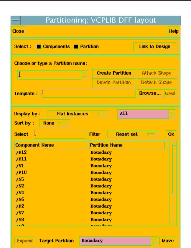
4. The Partitioning form appears.
December 2002 |
285 |
Product Version 5.0 |
Virtuoso XL Layout Editor User Guide
Using the Virtuoso Custom Placer
5.Click Link and then click anywhere in the layout cellview to link the Partitioning form to the layout.In the CIW a message appears telling you that the Partitioning Form is linked to the design “VCPLIB BUF layout”.
6.By default the Partition name is set to Boundary. To create a new partition name clear the text field and type in a user defined partition name and selectCreate Partition.
The new partition name appears in the cyclic field with a question mark next to the name. The question mark denotes that the partition does not have a shape attached to it.
7.To attach the softFence rectangle to the partition select Attach Shape and click to select the rectangle.
8.To add the devices to the partition change the Target Partition to the new partition name and select the devices in the Component Name list.
9.Select Move to move the devices into the partition. Notice that the components and partition are highlighted.
Loading the Template File
1.Click on the Browse button and the Open File form appears.
If you know the template file name you can type the file name in theTemplate text field.
2.Click on the directories in the left list box to descend into your file hierarchy until you reach the name of the template file to use.
The left and right arrows at the right side of the form let you go up and down in the file hierarchy.
3.Click on the name of the template file in the right list box to enter it in theName field.
4.Click OK.
Saving Partitions to a Template File
You can save the partition information from the cellview to a template file by using theDesign
– Save To Template command. Below is an example of the partition information that is saved to the template file.
partition_section(
connectivity "VCPLIB DFF schematic"
December 2002 |
286 |
Product Version 5.0 |