

Virtuoso XL Layout Editor User Guide
Generating Your Layout with Virtuoso XL Layout Editor
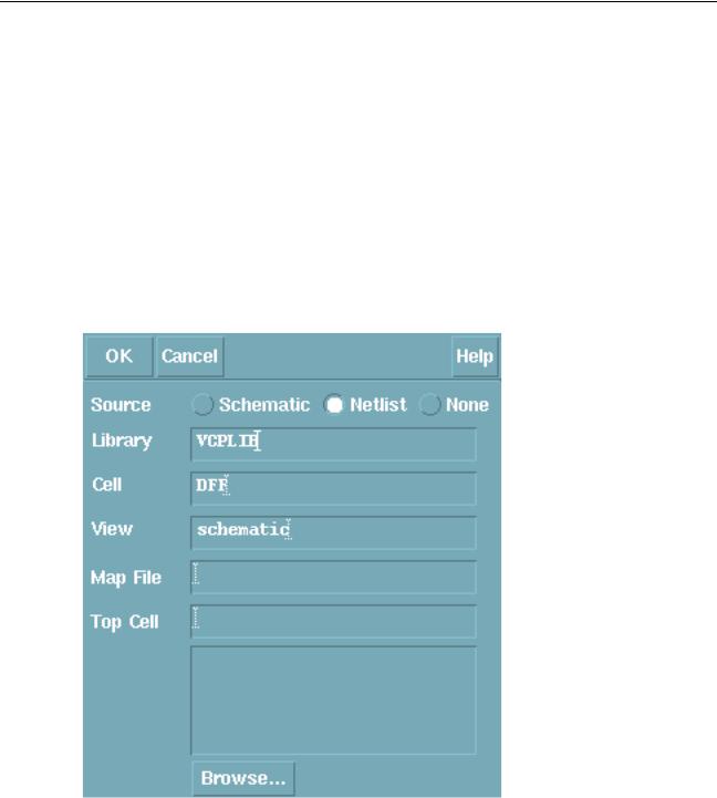
Connectivity Reference as a Netlist
The netlist syntax must comply with the guidelines defined in appendix B titledUsing Spice and CDL For Netlist Driven Layout Generation. If you do not follow these guidelines, then the layout may not reflect the full intent of the netlist.
The netlist can contain user defined properties and generic parameters that can be passed to the layout instance generated from Virtuoso XL. Any parameter of type String, Boolean, int, and float is supported.
If the connectivity reference is a netlist, choose Netlist.
The Define Connectivity Reference form changes to let you enter the Map File and the Top Cell of the netlist.
1.Type the name of a mapping file to import.
The mapping file lists model, cell (subcircuit), and instance properties and maps them to the names they have in the layout.
December 2002 |
143 |
Product Version 5.0 |

Virtuoso XL Layout Editor User Guide
Generating Your Layout with Virtuoso XL Layout Editor
You can also use the mapping file to map terminal names in the netlist (such as resistor terminal names Plus and Minus) to terminal names in the layout (such as resistor terminal names A and B), and parameter names in the netlist (such as the resistance value r) to parameter names in the layout (such as the resistance value R).
The Connectivity-Update-Source command loads the information in the mapping file into the cellview you specify on the form, overwriting any previously entered information. The mapping file structure, with an example, is shown in the next section.
You can click Browse to open the Library Browser to find a netlist and click on the netlist name to enter it in the Define Connectivity Reference form.
Mapping File Structure
The structure of the mapping file is as follows: the first section is the cell and model section which is mandatory(lxNetlistCellMap); the second section is optional and contains the instance mapping section (lxNetlistInstMap);
lxNetlistCellMap( (device_class
(device_type
(property) (property)
...
)
(property)
...
)
(property)
...
)lxNetlistInstMap( (device_hierarchical_name (property)
(property)
...
(property)
...
)
(device_hierarchical_name (property)
(property)
December 2002 |
144 |
Product Version 5.0 |

Virtuoso XL Layout Editor User Guide
Generating Your Layout with Virtuoso XL Layout Editor
...
(property)
...
)
)
where
■device_class is a string identifying a model or cell (subcircuit). If the device_type is specified, this parameter can be omitted. The format of thedevice_class is identical to the value field of the device“ _type”.
Note: device_class cannot be used anymore for all the model names of certain types (e.g. R for all resistors, M for MOS) because it is incompatible with the enhanced format.
■device_type identifies the model or cell (subcircuit) in the connectivity source hierarchy. It contains a keyword, a separator and value, for example, the name of the model or cell (subcircuit). The keyword is one of “MODEL”, “SUBCKT”, or “CELL”. The separator is the “=” character and the value is either a single string of characters (quoted or unquoted) that specify the model of subcircuit name for SPICE/CDL netlists or a quoted, space separated “lib cell” name when mapping composer schematic CELLS.
Note: When using the “device_class” field instead of the device_type, the field must always be quoted.
xNetlistCellMap(("nmos"
...
)
)
is equivalent to:
lxNetlistCellMap(
((MODEL=nmos
...
)
December 2002 |
145 |
Product Version 5.0 |

Virtuoso XL Layout Editor User Guide
Generating Your Layout with Virtuoso XL Layout Editor
...
)
)
For the following example:
lxNetlistCellMap("obsolete" ((CELL="mylib and"
...
)
(SUBCKT=AND2
...
)
)
)
the "obsolete" device_class is ignored.
■device_hierarchical_name is the hierarchical leaf instance name in forward slash (‘/’) separated name. For example, “/X1/X22/M3” is the name of the MOS transistor instantiated in the subcircuit X22, which is instantiated in subcircuit X1.
■property is a property. Properties can be defined in any number at any level inside the template, and inheritance rules apply to them. Therefore, properties defined at a high level apply globally to all devices defined at that level or lower, except where they are locally overwritten.
The following is the list of properties:
December 2002 |
146 |
Product Version 5.0 |

Virtuoso XL Layout Editor User Guide
Generating Your Layout with Virtuoso XL Layout Editor
useCell name definesname as the layout cell to be used to implement the device.
paramNameMap list defines a mapping table between the device parameters and the layout cell’s parameters. list is a list of pairs in the form device_param cell_param.
pinNameMap list defines a mapping table between the device pin names and the layout cell’s pin names. list is a list of pairs in the form device_pin cell_in.
paramSet list sets a list of parameters to the given values. The list contains elements of the type name type value, meaning that the value of name in the cell must be set to the value of the given type.
stopList list defineslist as the stop list.
ignoreNames list_of_names specifies instances to be ignored during layout generation. This property applies only at the top level of the design. If this property is used at lower levels, it still applies to only the top level and the software issues warnings to remind you of this.
ignoreCells list_of_names defines subcircuits whose instances are to be ignored during layout generation. This property applies only at the top level of the design. If it appears at a lower level, it still applies only to the top level and the software issues warnings to remind you of this.
ignoreParams list_of_params defines names of parameters to be ignored during layout generation. This property applies within the level it is defined in.
ignorePins list_of_pins defines names of pins to be ignored during layout generation. This property applies to all the instances within the level it is defined in
Note: The properties within a “model” block apply to that model only. The properties within a class apply to all the models in that section. The properties within the lxNetlistCellMap() block are global properties.
The order in which devices and properties are defined in the mapping file is irrelevant.
Example
lxNetlistCellMap(
("M"
(("MODEL" "=" "P") (useCell "pmos")
(paramNameMap ("WP" "w")("wp" "w")("LP" "l") ("lp" "l")) (paramSet ("l" "float" 1.1))
)
December 2002 |
147 |
Product Version 5.0 |

Virtuoso XL Layout Editor User Guide
Generating Your Layout with Virtuoso XL Layout Editor
((MODEL = Plow)
(useCell “pmos”)
)
(("MODEL" "=" "N") (useCell "nmos")
(paramNameMap ("WN" "w")("wn" "“w")("LN" "l")("ln" "l"))
)
(paramNameMap ("W" "w") ("L" "l") ("M" "m") ("C" "c") ("A" "a") ("P" "p") ("R" "r"))
(pinNameMap ("s" "S") ("g" "G") ("d" "D")("b" "B"))
(paramSet
("l" "float" 1.0) ("w" "float" 1.3)
("sourceContact?" "boolean" t) ("drainContact?" "boolean" t) ("showLabels?" "boolean" t)
)
(stopList "symbolic")
)
(stopList "layout compacted symbolic")
lxNetlistCellMap(
("M"
(("MODEL" "=" "P")
(useCell "pmos")
(paramNameMap ("WP" "w")("wp" "w")("LP" "l") ("lp" "l"))
(paramSet ("l" "float" 1.1))
)
(("MODEL" "=" "N")
(useCell "nmos")
(paramNameMap ("WN" "w")("wn" ""w")("LN" "l")("ln" "l"))
)
(paramNameMap ("W" "w") ("L" "l") ("M" "m")
("C" "c") ("A" "a") ("P" "p") ("R" "r"))
(pinNameMap ("s" "S") ("g" "G") ("d" "D")("b" "B"))
(paramSet
("l" "float" 1.0)
("w" "float" 1.3)
("sourceContact?" "boolean" t)
("drainContact?" "boolean" t)
("showLabels?" "boolean" t)
)
(stopList "symbolic")
)
(stopList "layout compacted symbolic")
December 2002 |
148 |
Product Version 5.0 |

Virtuoso XL Layout Editor User Guide
Generating Your Layout with Virtuoso XL Layout Editor
)
)
In this example, the device class “M” is ignored because 3 models are defined. The stop list
“layout compacted symbolic” applies to all devices except for the models “P” “Plow” and “N”, to which the stop list “symbolic” applies. Parameter 1 is set to 1.0 to both Plow and N models, except for the ones of model P, which is set to 1.1.
Defining the Design Boundary
When you initialize a layout, Virtuoso XL provides a design boundary.
To reset the default size for the design boundary, choose the layout window Design – Gen From Source command and set the options in the Boundary section of the Layout Generation Options form.
To stretch, move, or delete the design boundary, use the layout editor Edit commands. The design boundary must be a valid layer in the LSW and must be layer prBoundary or layer cellBoundary, or else it must have the purpose boundary (by).
To place all objects and pins inside the boundary, use the layout window Edit – Place from Schematic command.
To draw a new design boundary, follow these steps.
1.If you are using the Layout Generation Options form to generate a new layout, turn off
Boundary.
2.In the LSW, click on the prBoundary layer.
The boundary layer appears as the current layer at the top of the LSW. You can also use the layer cellBoundary from the Layout Generation Options form Boundary section Layer cyclic field.
3.From the layout window, choose Create – Rectangle or Create – Polygon.
4.Draw the design boundary in the layout window where you want it placed.
For a rectangular boundary, click to place one corner of the new boundary, drag the mouse to place the opposite corner, and release the mouse button.
For a polygonal boundary, use the cursor to click on the first point, each corner point, and end point (identical to the first point) of the polygon.
The new boundary appears in the layout window.
December 2002 |
149 |
Product Version 5.0 |