- •Contents
- •Preface
- •Related Documents
- •Typographic and Syntax Conventions
- •Introduction to the Virtuoso XL Layout Editor
- •Editing Your Technology File for Virtuoso XL Layout Editor
- •Sample Technology File
- •Virtuoso XL Technology File Requirements
- •Layer Rules
- •Devices
- •Physical Rules
- •Virtuoso XL Rules (lxRules)
- •Compactor Rules
- •Preparing Your Connectivity Source for the Virtuoso XL Layout Editor
- •Placing Design Elements
- •Using Design Variables
- •Netlist Processor Expressions
- •Analog Expression Language Expressions
- •Simulation Design Variables
- •Using One-to-Many Mapping
- •Iterated Instances and Bus Pins
- •Multiplication Factor (mfactor)
- •Series-Connection Factor (sfactor)
- •One-to-Many Assignment with the Update Device Correspondence
- •Using Many-to-Many or Many-to-One Mapping
- •Modifying Many-to-Many or Many-to-One Mapping Between Components
- •Deleting Many-to-Many or Many-to-One Mapping Between Components
- •Using Virtuoso XL Properties
- •Using the lxUseCell Property to Specify Layout Devices to Use
- •Using the lvsIgnore Property to Exclude Schematic Symbols
- •Using the lxlgnoredParams Property to Exclude Device Properties
- •Using the lxRemoveDevice property to Ignore Parasitic Devices
- •Using the lxViewList and lxStopList Properties to Prepare Hierarchical Designs
- •Using the lxCombination Property to Build Complex Devices
- •Preparing Instances and Pins in Your Layout for the Virtuoso XL Layout Editor
- •Preparing Pins for the Virtuoso XL Layout Editor
- •Preparing Pins for Permutability
- •Search Order Variable
- •Syntax
- •Macros
- •Setting the permuteRule Property in the Symbol Master
- •Setting the permuteRule Property in the Device Master
- •Setting the permuteRule Property in the Symbol Instance
- •Setting the permuteRule Property in the Device Instance
- •Setting the permuteRule Property in the Component Description Format
- •Preparing Instances for Hierarchical Connectivity Checking
- •Setting Up Your Desktop
- •Customizing Your Desktop Layout
- •Using Multiple Cellviews
- •Printing to the Command Interpreter Window
- •Changing Display Colors
- •Using Bindkeys
- •Displaying Bindkeys
- •Loading Virtuoso XL Bindkeys
- •Setting Environment Variables
- •Information About Online Forms
- •Layout XL Options Form
- •Introduction to Abutment
- •Abutment Requirements
- •Setting Up Cells for Abutment
- •abutAccessDir
- •abutClass
- •Steps in Auto-Abutment
- •Sample Parameterized Cells Set Up for Abutment
- •Example 1
- •Example 2
- •Creating CMOS Pcells to Use with Abutment
- •autoAbutment Properties
- •The abutMosStretchMat Property
- •abutMosStretchMat Rules for MOS Abutment
- •Example Code Setting MOS Abutment Properties
- •Setting Environment Variables for Abutment
- •Move Together
- •Constraint Assisted
- •Using Device Abutment
- •Generating Your Layout with Virtuoso XL Layout Editor
- •Starting Virtuoso XL from the Schematic
- •Importing a Netlist for a Connectivity Reference
- •Starting Virtuoso XL from the Layout View
- •Connectivity Reference as a Netlist
- •Mapping File Structure
- •Working with Template Files
- •Saving Form Contents
- •Loading Template Files
- •Modifying Templates
- •Loading Template Files
- •Creating Template Files
- •Template File Syntax
- •General Syntax Rules
- •Boundaries Section
- •I/O Pins Section
- •Sample Template
- •Generating a Layout with Components Not Placed (Gen From Source)
- •Moving Components from the Schematic into the Layout (Pick from Schematic)
- •Placing a Group of Schematic Elements Together
- •Placing Individual Components
- •Generating Pins
- •Viewing Unplaced Instances/Pins
- •Viewing in Place
- •Manually Abutting Devices Using Pick from Schematic
- •Cloning Components
- •Cloning
- •Troubleshooting
- •Cloning Using Multiple Cellviews
- •Using Correspondence Points
- •Information About Online Forms
- •Add Correspondence Pairs Form
- •Cloning Form
- •Correspondence Pairs Form
- •Import XL Netlist Form
- •Layout Generation Options Form
- •Open File Form
- •Pick from Schematic Form
- •Remove Correspondence Components Form
- •Set Pin Label Text Style Form
- •Startup Option Form
- •Template File Form
- •Editing Your Layout with Virtuoso XL Layout Editor
- •Identifying Incomplete Nets
- •Moving Objects Manually in the Virtuoso XL Layout Editor
- •Moving Objects Using Move Options
- •Setting the Move Form to Appear Automatically
- •Aligning Objects
- •Post Selecting Devices
- •PreSelecting Devices
- •Swapping Components
- •Permuting Component Pins
- •Permuting Pins Manually
- •Checking Permutation Information
- •Using Device Locking
- •Using Automatic Spacing
- •Using Interactive Device Abutment
- •Setting Component Types
- •About Component Types
- •MOS Transistor Stacking and Folding Parameters
- •Modifying a Component Type
- •Using Transistor Chaining
- •Using Transistor Folding
- •Controlling the Folding Grid
- •Folding Transistors
- •Adding Instances to a Layout
- •Adding Pins to a Layout
- •Assigning Pins to a Net
- •Maintaining Connectivity When Editing a Flattened Pcell
- •Information About Online Forms
- •Assign Nets Form
- •Edit Component Types Form
- •Move Form
- •Set Transistor Folding Form
- •Show Incomplete Nets Form
- •Stretch Form
- •Virtuoso XL Alignment Form
- •Using the Virtuoso Custom Placer
- •Overview
- •Main Features
- •Place Menu Command Summary
- •Other Commands Used with the Virtuoso custom placer
- •Placement Styles
- •Setting Up the Virtuoso XL Layout Editor for Placement
- •Identifying the Placement Translation Rules
- •Setting Cadence Design Framework II Environment Variables
- •Setting Environment Variables for the Virtuoso Custom Router and Placer
- •Setting MOS Chaining and Folding Parameters
- •Abutting Standard Cells
- •Using Auto-Abutment During Placement
- •Placement Constraints
- •Constraint Manager Geometric Constraints
- •Pin Placement Constraints
- •Constraint Limitations
- •Placement Parameters and Component Types
- •MOS Transistor Chaining and Folding Parameters
- •Pin Placement
- •Assigning Pins to an Edge
- •Assigning Pins to a Fixed Position
- •Railing Pins
- •Loading the Template File
- •Assigning Spacing Between Pins
- •Saving Pin Placement to a Template File
- •Partitioning the Design
- •Creating a Partition
- •Loading the Template File
- •Saving Partitions to a Template File
- •Setting Placement Planning
- •Assisted CMOS Placement
- •Choose Component Types Form
- •Running the Virtuoso Custom Placer
- •Prerequisites to Placement
- •Running the Virtuoso Custom Placer: Initial Placement
- •Stopping the Placer
- •Running Load Balancing Service (LBS)
- •Troubleshooting Placement Results
- •Running the Virtuoso Custom Placer: Detailed Placement
- •Showing Congestions
- •Information About Forms
- •Auto Placer Form
- •Partitioning Form
- •Choose Component Types Form
- •Pin Placement Form
- •Load Template File Form
- •Placement Planning Form (Assisted CMOS)
- •Placement Planning Form (Assisted Standard Cell)
- •Placement Planning Form (Assisted Mixed CMOS/Standard-Cell)
- •Preparing Your Design for Routing in the Virtuoso XL Layout Editor
- •Understanding Connectivity
- •Pseudo-Parallel Connections
- •Selecting Layers
- •Changing Layers
- •Connecting Nets
- •Creating Paths
- •Connecting Nets with Path Stitching
- •Connecting Nets with Design Shapes
- •Checking Connectivity with Flight Lines
- •Checking Connectivity with Markers
- •Finding Markers
- •Explaining Markers
- •Deleting Single Markers
- •Deleting All Markers
- •Using the Virtuoso Compactor on a Routed Design
- •Overview
- •Main Features
- •Wire Editing Commands
- •Virtuoso Custom Router to Virtuoso XL Command Mapping
- •Prerequisites
- •Rule Information
- •Net Connectivity Information
- •Routing Area Boundary
- •Enabling Wire Editing
- •Toggling Between Virtuoso XL and Wire Editing Enabled
- •Loading ASCII Rules Files
- •The Wire Editing Environment
- •Status Banner
- •Preview Wires and Routing Aids
- •Mouse Button Behavior
- •Using Environment Variables
- •Routing Paths
- •Routing a Single Path
- •Routing Multiple Paths
- •Preventing and Checking Design Rule Violations
- •Interactive Checking
- •Same Net Checking
- •Checking Regions
- •Checking Route and Pin Violations
- •Routing Options and Styles
- •Matching Path Width and Pin Widths
- •Matching Path Width and Pin Widths for Multiple Paths
- •Gathering Bus Wires
- •Spacing for Gathered Bus Wires
- •Overriding Bus Spacing
- •Rotating the Bus Cursor
- •Cycling the Control Wire
- •Allowing Redundant Wiring
- •Allowing Orthogonal Jogs
- •Route To Cursor
- •Allow Floating Nets
- •Connecting Multiple Component Pins
- •Pushing Routes and Components
- •Routing Shielded Nets
- •Routing Tandem Layer Pairs
- •Using Vias
- •Changing Layers and Adding Vias
- •Using Vias Patterns on Multiple Paths
- •Legal Via Sites
- •Rotating Vias
- •Pseudo Vias
- •Editing Routed Connections
- •Stretching Paths and Vias
- •Splitting and Stretching Paths
- •Copying Routes
- •Using Critic Wire
- •Compacting Paths Using Pull
- •Displaying Reports
- •Displaying Routing Status Reports
- •Displaying Network Reports
- •Displaying Component Reports
- •Displaying Net Reports
- •Creating Rules Reports
- •Search Reports
- •Saving Reports
- •Setting Constraints
- •Using the Virtuoso Constraint Manager
- •Using .do Files
- •About the Forms
- •Add Via Form
- •Check Routes Form
- •Create Path Form
- •Find File Form
- •Layout
- •Reports Form
- •Route Options Form
- •Save As Form
- •Search Form
- •Split Form
- •Via Pattern Pop-up
- •Reports
- •Route Status Report Window
- •Network Report Window
- •Instance Report Window
- •Net Report Window
- •Rules Report Window
- •Setting Environment Variables
- •Troubleshooting
- •Finding Design Elements (Probing)
- •Probing Hierarchical Designs
- •Removing Probes
- •Exiting the Probe Command
- •Showing the Options Form
- •Checking Shorts and Opens
- •Comparing Design Elements and Parameters (Checking against the Connectivity Source)
- •Information About Online Forms
- •Probe Options Form
- •Updating Design Data in Virtuoso XL
- •Updating Layout Parameters
- •Updating Schematic Parameters
- •Updating Device Correspondence
- •Creating Device Correspondence
- •Needed Mode
- •Computer Aided Mode
- •Updating the Connectivity Reference
- •Changing the Device (Instance) View
- •Information About Online Forms
- •Change Instance View Form
- •Create Device Correspondence
- •Problems with the Interface
- •Invalid Markers from Previous Software Versions
- •Options Form Does Not Appear
- •Virtuoso XL Performance Is Slow
- •Problems with Editing
- •Components Move Slowly
- •Extra Probes Appear
- •Layout Generation Options Form Does Not Keep Values from the Last Entry
- •Parameters Not Updated
- •Schematic Not Editable
- •Warning to Update Your Design Appears at Startup
- •Problems with Connectivity
- •Connections Not Made
- •Incomplete Nets Command Does Not Recognize Connected Pins and Nets
- •Markers for Nonexistent Overlaps and Shorts Appear
- •Path Ends Not Accepted
- •Placement and Routing Do Not Run
- •Virtuoso XL Does Not Recognize Physical Vias
- •Moving Software Executables To a New Location
- •Environment Variables
- •Virtuoso XL Layout Editor
- •alignApplySeparation
- •alignApplySpacings
- •alignDirection
- •alignLayer
- •alignMethod
- •alignSelectionMode
- •alignSeparation
- •allowRotation
- •autoAbutment
- •autoArrange
- •autoPermutePins
- •autoSpace
- •checkTimeStamps
- •ciwWindow
- •compTypeRefLibs
- •constraintAssistedMode
- •createBoundaryLabel
- •crossSelect
- •extractEnable
- •extractStopLevel
- •globalPlacement
- •ignoredParams
- •ignoreNames
- •incNetCycleHilite
- •incNetHiliteLayer
- •infoWindow
- •initAspectRatio
- •initAspectRatioOption
- •initBoundaryLayer
- •initCreateBoundary
- •initCreateInstances
- •initCreateMTM
- •initCreatePins
- •initDoFolding
- •initDoStacking
- •initEstimateArea
- •initGlobalNetPins
- •initIOLabelType
- •initIOPinLayer
- •initIOPinName
- •initPinHeight
- •initPinMultiplicity
- •initPinWidth
- •initPrBoundaryH
- •initPrBoundaryW
- •initSymbolicPins
- •initUtilization
- •layoutWindow
- •lswWindow
- •lxAllowPseudoParallelNets
- •lxDeltaWidth
- •lxFingeringNames
- •lxGenerationOrientation
- •lxGenerationTopLevelOnly
- •lxInitResetSource
- •lxStackMinimalFolding
- •lxStackPartitionParameters
- •lxWidthTolerance
- •maintainConnections
- •mfactorNames
- •mfactorSplit
- •moveAsGroup
- •openWindow
- •optimizePlacement
- •paramTolerance
- •pathProbe
- •pathPurposeList
- •pathSwitchLayer
- •pathSwitchPurpose
- •preserveTerminalContacts
- •probeCycleHilite
- •probeDevice
- •probeHiliteLayer
- •probeInfoInCIW
- •probeNet
- •probePin
- •rowGroundLayer
- •rowGroundName
- •rowGroundWidth
- •rowPowerLayer
- •rowPowerName
- •rowPowerWidth
- •rowSupplyPosition
- •rowSupplySpacing
- •rowMOSSupplyPattern
- •rowSTDAllowFlip
- •rowSTDSupplyPattern
- •rulesFile
- •runTime
- •saveAs
- •saveAsCellName
- •saveAsLibName
- •saveAsViewName
- •schematicWindow
- •setPPConn
- •sfactorNames
- •sfactorParam
- •showIncNetEnable
- •stopList
- •templateFileName
- •traverseMixedHierarchies
- •updateReplacesMasters
- •updateWithMarkers
- •vcpConductorDepth
- •vcpKeepoutDepth
- •viewList
- •Wire Editor
- •allowFloatingNets
- •allowJogs
- •allowRedundantWiring
- •autoAdjustLength
- •autoShield
- •busOverride
- •busOverrideValue
- •busWireSpacing
- •busWireSpacingType
- •checkCornerCorner
- •checkCrosstalk
- •checkLength
- •checkLimitWay
- •checkMaxProcessWireWidth
- •checkMaxStackViaDepth
- •checkMaxTotalVia
- •checkMinMaskEdgeLength
- •checkMinProcessWireWidth
- •checkMiter
- •checkNetOrder
- •checkOffManGridPin
- •checkOffWireGridPin
- •checkPinSpacing
- •checkPolygonWire
- •checkProtected
- •checkReentrantPath
- •checkRegion
- •checkSameNet
- •checkSegment
- •checkStub
- •checkUseLayers
- •checkUseVias
- •checkWireExtension
- •doFile
- •enableBusRouting
- •enableTandemPair
- •gatherBusWires
- •inaccessiblePin
- •interactiveChecking
- •matchPinWidth
- •matchPinWidthValue
- •matchWireWidth
- •multiplePinsConnection
- •pinLargerMaxProcessWidth
- •pinSmallerMinProcessWidth
- •pushComponent
- •pushRouting
- •routeAsManyAsPossible
- •routeToCursor
- •routeToCursorStyle
- •sameNetChecking
- •showTimingMeter
- •showTimingOctagon
- •snapToPinOrigin
- •useDoFile
- •useRulesFile
- •viaAssistance
- •viaPattern
- •Private Environment Variables
- •Virtuoso XL Command Quick Reference
- •Using Spice and CDL For Netlist Driven Layout Generation
- •Introduction
- •Specifying Spice Designs
- •Cell Creation Rules
- •Character Considerations
- •Spice Statements
- •File Level Statements
- •Statements Allowed at File Level or within a Subckt Cell or a Top Level Cell
- •Statements Allowed within a Subckt Cell or a Top Level Cell
- •Spice Design Example
- •CDL Design Example
- •Parameter Resolution
- •Parameter Levels
- •Resolving Parameters
- •Putting the Rules Together (Examples)
- •Parameter Scaling
- •Complete ibuf Example Results
- •Virtuoso XL .do File Commands
- •Rule Hierarchy
- •circuit
- •Syntax
- •Example
- •Syntax
- •Example
- •limit
- •Syntax
- •Example
- •rule
- •Syntax
- •Example
- •Syntax
Virtuoso XL Layout Editor User Guide
Generating Your Layout with Virtuoso XL Layout Editor
Note: When placing components within the design boundary, the Place As In Schematic command might cause the components to overlap, resulting in shorts. When you create a short, Virtuoso XL displays a marker over the short.
Virtuoso XL does not compact the layout, so the placement of components might not meet
Design Rule Checker (DRC) or other design requirements.
Constraints entered using the Constraint Manager are not observed by the Place As In
Schematic command.
Moving Components from the Schematic into the Layout (Pick from Schematic)
To place devices and/or pins directly from the schematic into the layout use the Create-Pick from Schematic command. If your connectivity reference is not a schematic, you cannot use this command.
Placing a Group of Schematic Elements Together
Use the Group As In Schematic option to place the instance/pins in the layout with the same relative position as in the schematic.
1.From the layout window, choose Create – Pick from Schematic.
The first time you open a new design and use this command, theDefine Connectivity Reference form appears.
2.If the Define Connectivity Reference form appears, type the library, cell, and view name of the schematic from which you want to pick elements to place in the layout (if this information is different from the information that appears by default in the form) and click
OK.
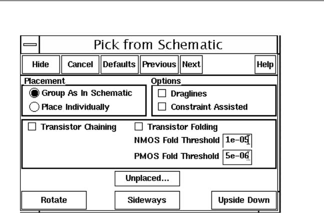
3.In the Pick from Schematic form, turn on Group As In Schematic. In this mode, you cannot change the parameters of the components.
4.Select a group of components (or all the components) in the schematic.
5.If some components in the schematic are already present in the layout, you cannot select them; only those components not yet placed can be selected.
December 2002 |
173 |
Product Version 5.0 |
Virtuoso XL Layout Editor User Guide
Generating Your Layout with Virtuoso XL Layout Editor
The Pick from Schematic form appears.
6.Turn on the options you want.
Draglines displays rubberbanding lines that connect pins of the object you are moving to pins of the nearest objects.
Constraint Assisted allows objects to be moved only in ways that satisfy the constraints entered using the Constraint Manager, once the object has satisfied the constraint.
Transistor Chaining allows MOS transistors (or fingers of folded transistors) to be automatically abutted to form a stack.
Transistor Folding allows MOS transistors to be automatically divided into fingers for optimum area usage.
NMOS Fold Threshold lets you type in the maximum size of the folded NMOS transistor. This value defaults to the lxMaxWidth value set on the connectivity source component.
Changing this value overwrites the lxMaxWidth value you entered in the Edit Component Type form.
December 2002 |
174 |
Product Version 5.0 |
Virtuoso XL Layout Editor User Guide
Generating Your Layout with Virtuoso XL Layout Editor
PMOS Fold Threshold lets you type in the maximum size of the folded PMOS transistor. This value defaults to the lxMaxWidth value set on the connectivity source component.
Changing this value overwrites the lxMaxWidth value you entered in the Edit
Component Type form.
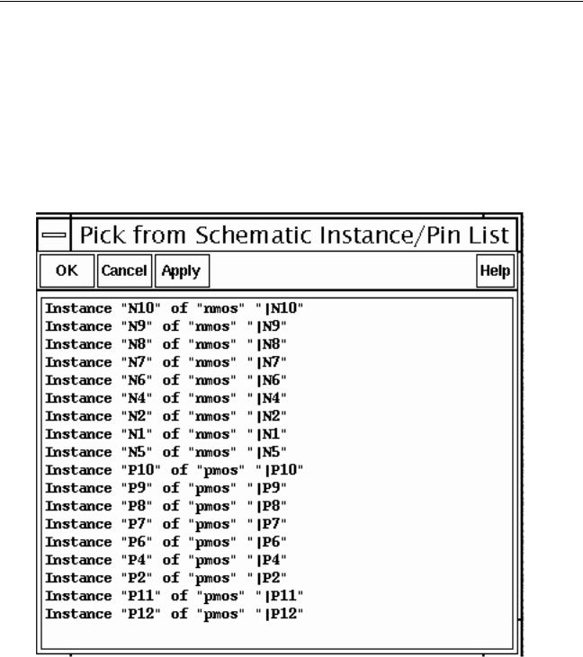
7.To see a list of the components in the schematic that are not yet placed in the layout, click
Unplaced.
The Pick from Schematic Instance/Pin List appears.
8.In the list box, click on the names of the devices you want to place and click Apply or OK.
9.Move the cursor into the layout window and click.
The group of components selected are placed in the layout in the same relative position as in the schematic.
December 2002 |
175 |
Product Version 5.0 |
Virtuoso XL Layout Editor User Guide
Generating Your Layout with Virtuoso XL Layout Editor
Only components not yet present in the layout can be placed.
Placing Individual Components
To place individual components from the schematic in the layout, follow these steps.
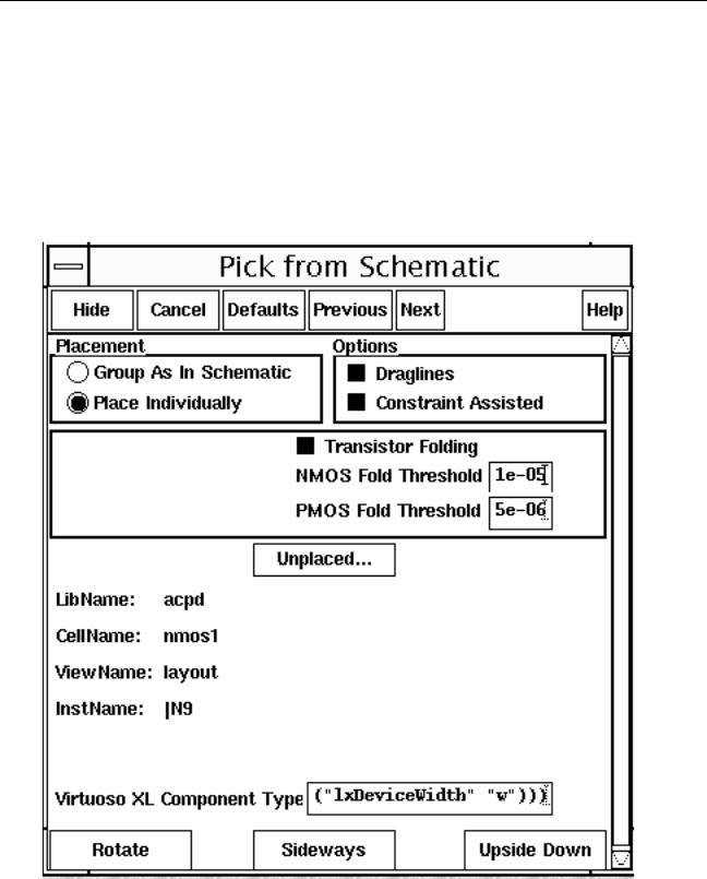
1.In the Pick from Schematic form, turn on Place Individually.
The Pick from Schematic form changes to let you select individual instances.
December 2002 |
176 |
Product Version 5.0 |
Virtuoso XL Layout Editor User Guide
Generating Your Layout with Virtuoso XL Layout Editor
Note: The Place Individually option does not allow you to chain devices. Transistor
Chaining is only available with the Group As In Schematic option.
2.In the schematic, click on the component or group of components you want to place in the layout.
To select multiple components, click on the first object to select it andShift click on the other objects or click and drag over the objects. You can deselect objects with Control click.
Selected objects in the schematic remain highlighted until they are deselected or placed in the layout.
You cannot select objects in the schematic if objects with the same name are already present in the layout.
3.To automatically fold MOS devices into divided fingers for optimum are usage turn on the
Transistor Folding option.
NMOS Fold Threshold lets you type in the maximum size of the folded NMOS transistor. This value defaults to the lxMaxWidth value set on the connectivity source component.
PMOS Fold Threshold lets you type in the maximum size of the folded PMOS transistor. This value defaults to the lxMaxWidth value set on the connectivity source component.
Important
When the Transistor Folding option is turned on the device properties do not appear at the bottom of the Pick from Schematic form. If you need to update any of the device properties turn off Transistor Folding.
4.Select Unplaced to view the Pick from Schematic Instance/Pin List. Select the pin or instance and click Apply. The pin or instance will be selected in the schematic window.
5.Move the cursor into the layout window and the Pick from Schematic form updates with the Library, Cell, View, and InstName.
The Pick from Schematic form updates to show the parameters associated with the component currently being placed.
6.The component to be placed first is highlighted in the schematic in the color assigned to the hilite drawing2 layer. Selected instances that have not yet been placed are highlighted in the color assigned to the hilite drawing layer.
The outline of the component follows the cursor in the layout. Rubberbanding drag lines, showing connectivity to already placed components, follow the component outline.
December 2002 |
177 |
Product Version 5.0 |