- •Contents
- •Preface
- •Related Documents
- •Typographic and Syntax Conventions
- •Introduction to the Virtuoso XL Layout Editor
- •Editing Your Technology File for Virtuoso XL Layout Editor
- •Sample Technology File
- •Virtuoso XL Technology File Requirements
- •Layer Rules
- •Devices
- •Physical Rules
- •Virtuoso XL Rules (lxRules)
- •Compactor Rules
- •Preparing Your Connectivity Source for the Virtuoso XL Layout Editor
- •Placing Design Elements
- •Using Design Variables
- •Netlist Processor Expressions
- •Analog Expression Language Expressions
- •Simulation Design Variables
- •Using One-to-Many Mapping
- •Iterated Instances and Bus Pins
- •Multiplication Factor (mfactor)
- •Series-Connection Factor (sfactor)
- •One-to-Many Assignment with the Update Device Correspondence
- •Using Many-to-Many or Many-to-One Mapping
- •Modifying Many-to-Many or Many-to-One Mapping Between Components
- •Deleting Many-to-Many or Many-to-One Mapping Between Components
- •Using Virtuoso XL Properties
- •Using the lxUseCell Property to Specify Layout Devices to Use
- •Using the lvsIgnore Property to Exclude Schematic Symbols
- •Using the lxlgnoredParams Property to Exclude Device Properties
- •Using the lxRemoveDevice property to Ignore Parasitic Devices
- •Using the lxViewList and lxStopList Properties to Prepare Hierarchical Designs
- •Using the lxCombination Property to Build Complex Devices
- •Preparing Instances and Pins in Your Layout for the Virtuoso XL Layout Editor
- •Preparing Pins for the Virtuoso XL Layout Editor
- •Preparing Pins for Permutability
- •Search Order Variable
- •Syntax
- •Macros
- •Setting the permuteRule Property in the Symbol Master
- •Setting the permuteRule Property in the Device Master
- •Setting the permuteRule Property in the Symbol Instance
- •Setting the permuteRule Property in the Device Instance
- •Setting the permuteRule Property in the Component Description Format
- •Preparing Instances for Hierarchical Connectivity Checking
- •Setting Up Your Desktop
- •Customizing Your Desktop Layout
- •Using Multiple Cellviews
- •Printing to the Command Interpreter Window
- •Changing Display Colors
- •Using Bindkeys
- •Displaying Bindkeys
- •Loading Virtuoso XL Bindkeys
- •Setting Environment Variables
- •Information About Online Forms
- •Layout XL Options Form
- •Introduction to Abutment
- •Abutment Requirements
- •Setting Up Cells for Abutment
- •abutAccessDir
- •abutClass
- •Steps in Auto-Abutment
- •Sample Parameterized Cells Set Up for Abutment
- •Example 1
- •Example 2
- •Creating CMOS Pcells to Use with Abutment
- •autoAbutment Properties
- •The abutMosStretchMat Property
- •abutMosStretchMat Rules for MOS Abutment
- •Example Code Setting MOS Abutment Properties
- •Setting Environment Variables for Abutment
- •Move Together
- •Constraint Assisted
- •Using Device Abutment
- •Generating Your Layout with Virtuoso XL Layout Editor
- •Starting Virtuoso XL from the Schematic
- •Importing a Netlist for a Connectivity Reference
- •Starting Virtuoso XL from the Layout View
- •Connectivity Reference as a Netlist
- •Mapping File Structure
- •Working with Template Files
- •Saving Form Contents
- •Loading Template Files
- •Modifying Templates
- •Loading Template Files
- •Creating Template Files
- •Template File Syntax
- •General Syntax Rules
- •Boundaries Section
- •I/O Pins Section
- •Sample Template
- •Generating a Layout with Components Not Placed (Gen From Source)
- •Moving Components from the Schematic into the Layout (Pick from Schematic)
- •Placing a Group of Schematic Elements Together
- •Placing Individual Components
- •Generating Pins
- •Viewing Unplaced Instances/Pins
- •Viewing in Place
- •Manually Abutting Devices Using Pick from Schematic
- •Cloning Components
- •Cloning
- •Troubleshooting
- •Cloning Using Multiple Cellviews
- •Using Correspondence Points
- •Information About Online Forms
- •Add Correspondence Pairs Form
- •Cloning Form
- •Correspondence Pairs Form
- •Import XL Netlist Form
- •Layout Generation Options Form
- •Open File Form
- •Pick from Schematic Form
- •Remove Correspondence Components Form
- •Set Pin Label Text Style Form
- •Startup Option Form
- •Template File Form
- •Editing Your Layout with Virtuoso XL Layout Editor
- •Identifying Incomplete Nets
- •Moving Objects Manually in the Virtuoso XL Layout Editor
- •Moving Objects Using Move Options
- •Setting the Move Form to Appear Automatically
- •Aligning Objects
- •Post Selecting Devices
- •PreSelecting Devices
- •Swapping Components
- •Permuting Component Pins
- •Permuting Pins Manually
- •Checking Permutation Information
- •Using Device Locking
- •Using Automatic Spacing
- •Using Interactive Device Abutment
- •Setting Component Types
- •About Component Types
- •MOS Transistor Stacking and Folding Parameters
- •Modifying a Component Type
- •Using Transistor Chaining
- •Using Transistor Folding
- •Controlling the Folding Grid
- •Folding Transistors
- •Adding Instances to a Layout
- •Adding Pins to a Layout
- •Assigning Pins to a Net
- •Maintaining Connectivity When Editing a Flattened Pcell
- •Information About Online Forms
- •Assign Nets Form
- •Edit Component Types Form
- •Move Form
- •Set Transistor Folding Form
- •Show Incomplete Nets Form
- •Stretch Form
- •Virtuoso XL Alignment Form
- •Using the Virtuoso Custom Placer
- •Overview
- •Main Features
- •Place Menu Command Summary
- •Other Commands Used with the Virtuoso custom placer
- •Placement Styles
- •Setting Up the Virtuoso XL Layout Editor for Placement
- •Identifying the Placement Translation Rules
- •Setting Cadence Design Framework II Environment Variables
- •Setting Environment Variables for the Virtuoso Custom Router and Placer
- •Setting MOS Chaining and Folding Parameters
- •Abutting Standard Cells
- •Using Auto-Abutment During Placement
- •Placement Constraints
- •Constraint Manager Geometric Constraints
- •Pin Placement Constraints
- •Constraint Limitations
- •Placement Parameters and Component Types
- •MOS Transistor Chaining and Folding Parameters
- •Pin Placement
- •Assigning Pins to an Edge
- •Assigning Pins to a Fixed Position
- •Railing Pins
- •Loading the Template File
- •Assigning Spacing Between Pins
- •Saving Pin Placement to a Template File
- •Partitioning the Design
- •Creating a Partition
- •Loading the Template File
- •Saving Partitions to a Template File
- •Setting Placement Planning
- •Assisted CMOS Placement
- •Choose Component Types Form
- •Running the Virtuoso Custom Placer
- •Prerequisites to Placement
- •Running the Virtuoso Custom Placer: Initial Placement
- •Stopping the Placer
- •Running Load Balancing Service (LBS)
- •Troubleshooting Placement Results
- •Running the Virtuoso Custom Placer: Detailed Placement
- •Showing Congestions
- •Information About Forms
- •Auto Placer Form
- •Partitioning Form
- •Choose Component Types Form
- •Pin Placement Form
- •Load Template File Form
- •Placement Planning Form (Assisted CMOS)
- •Placement Planning Form (Assisted Standard Cell)
- •Placement Planning Form (Assisted Mixed CMOS/Standard-Cell)
- •Preparing Your Design for Routing in the Virtuoso XL Layout Editor
- •Understanding Connectivity
- •Pseudo-Parallel Connections
- •Selecting Layers
- •Changing Layers
- •Connecting Nets
- •Creating Paths
- •Connecting Nets with Path Stitching
- •Connecting Nets with Design Shapes
- •Checking Connectivity with Flight Lines
- •Checking Connectivity with Markers
- •Finding Markers
- •Explaining Markers
- •Deleting Single Markers
- •Deleting All Markers
- •Using the Virtuoso Compactor on a Routed Design
- •Overview
- •Main Features
- •Wire Editing Commands
- •Virtuoso Custom Router to Virtuoso XL Command Mapping
- •Prerequisites
- •Rule Information
- •Net Connectivity Information
- •Routing Area Boundary
- •Enabling Wire Editing
- •Toggling Between Virtuoso XL and Wire Editing Enabled
- •Loading ASCII Rules Files
- •The Wire Editing Environment
- •Status Banner
- •Preview Wires and Routing Aids
- •Mouse Button Behavior
- •Using Environment Variables
- •Routing Paths
- •Routing a Single Path
- •Routing Multiple Paths
- •Preventing and Checking Design Rule Violations
- •Interactive Checking
- •Same Net Checking
- •Checking Regions
- •Checking Route and Pin Violations
- •Routing Options and Styles
- •Matching Path Width and Pin Widths
- •Matching Path Width and Pin Widths for Multiple Paths
- •Gathering Bus Wires
- •Spacing for Gathered Bus Wires
- •Overriding Bus Spacing
- •Rotating the Bus Cursor
- •Cycling the Control Wire
- •Allowing Redundant Wiring
- •Allowing Orthogonal Jogs
- •Route To Cursor
- •Allow Floating Nets
- •Connecting Multiple Component Pins
- •Pushing Routes and Components
- •Routing Shielded Nets
- •Routing Tandem Layer Pairs
- •Using Vias
- •Changing Layers and Adding Vias
- •Using Vias Patterns on Multiple Paths
- •Legal Via Sites
- •Rotating Vias
- •Pseudo Vias
- •Editing Routed Connections
- •Stretching Paths and Vias
- •Splitting and Stretching Paths
- •Copying Routes
- •Using Critic Wire
- •Compacting Paths Using Pull
- •Displaying Reports
- •Displaying Routing Status Reports
- •Displaying Network Reports
- •Displaying Component Reports
- •Displaying Net Reports
- •Creating Rules Reports
- •Search Reports
- •Saving Reports
- •Setting Constraints
- •Using the Virtuoso Constraint Manager
- •Using .do Files
- •About the Forms
- •Add Via Form
- •Check Routes Form
- •Create Path Form
- •Find File Form
- •Layout
- •Reports Form
- •Route Options Form
- •Save As Form
- •Search Form
- •Split Form
- •Via Pattern Pop-up
- •Reports
- •Route Status Report Window
- •Network Report Window
- •Instance Report Window
- •Net Report Window
- •Rules Report Window
- •Setting Environment Variables
- •Troubleshooting
- •Finding Design Elements (Probing)
- •Probing Hierarchical Designs
- •Removing Probes
- •Exiting the Probe Command
- •Showing the Options Form
- •Checking Shorts and Opens
- •Comparing Design Elements and Parameters (Checking against the Connectivity Source)
- •Information About Online Forms
- •Probe Options Form
- •Updating Design Data in Virtuoso XL
- •Updating Layout Parameters
- •Updating Schematic Parameters
- •Updating Device Correspondence
- •Creating Device Correspondence
- •Needed Mode
- •Computer Aided Mode
- •Updating the Connectivity Reference
- •Changing the Device (Instance) View
- •Information About Online Forms
- •Change Instance View Form
- •Create Device Correspondence
- •Problems with the Interface
- •Invalid Markers from Previous Software Versions
- •Options Form Does Not Appear
- •Virtuoso XL Performance Is Slow
- •Problems with Editing
- •Components Move Slowly
- •Extra Probes Appear
- •Layout Generation Options Form Does Not Keep Values from the Last Entry
- •Parameters Not Updated
- •Schematic Not Editable
- •Warning to Update Your Design Appears at Startup
- •Problems with Connectivity
- •Connections Not Made
- •Incomplete Nets Command Does Not Recognize Connected Pins and Nets
- •Markers for Nonexistent Overlaps and Shorts Appear
- •Path Ends Not Accepted
- •Placement and Routing Do Not Run
- •Virtuoso XL Does Not Recognize Physical Vias
- •Moving Software Executables To a New Location
- •Environment Variables
- •Virtuoso XL Layout Editor
- •alignApplySeparation
- •alignApplySpacings
- •alignDirection
- •alignLayer
- •alignMethod
- •alignSelectionMode
- •alignSeparation
- •allowRotation
- •autoAbutment
- •autoArrange
- •autoPermutePins
- •autoSpace
- •checkTimeStamps
- •ciwWindow
- •compTypeRefLibs
- •constraintAssistedMode
- •createBoundaryLabel
- •crossSelect
- •extractEnable
- •extractStopLevel
- •globalPlacement
- •ignoredParams
- •ignoreNames
- •incNetCycleHilite
- •incNetHiliteLayer
- •infoWindow
- •initAspectRatio
- •initAspectRatioOption
- •initBoundaryLayer
- •initCreateBoundary
- •initCreateInstances
- •initCreateMTM
- •initCreatePins
- •initDoFolding
- •initDoStacking
- •initEstimateArea
- •initGlobalNetPins
- •initIOLabelType
- •initIOPinLayer
- •initIOPinName
- •initPinHeight
- •initPinMultiplicity
- •initPinWidth
- •initPrBoundaryH
- •initPrBoundaryW
- •initSymbolicPins
- •initUtilization
- •layoutWindow
- •lswWindow
- •lxAllowPseudoParallelNets
- •lxDeltaWidth
- •lxFingeringNames
- •lxGenerationOrientation
- •lxGenerationTopLevelOnly
- •lxInitResetSource
- •lxStackMinimalFolding
- •lxStackPartitionParameters
- •lxWidthTolerance
- •maintainConnections
- •mfactorNames
- •mfactorSplit
- •moveAsGroup
- •openWindow
- •optimizePlacement
- •paramTolerance
- •pathProbe
- •pathPurposeList
- •pathSwitchLayer
- •pathSwitchPurpose
- •preserveTerminalContacts
- •probeCycleHilite
- •probeDevice
- •probeHiliteLayer
- •probeInfoInCIW
- •probeNet
- •probePin
- •rowGroundLayer
- •rowGroundName
- •rowGroundWidth
- •rowPowerLayer
- •rowPowerName
- •rowPowerWidth
- •rowSupplyPosition
- •rowSupplySpacing
- •rowMOSSupplyPattern
- •rowSTDAllowFlip
- •rowSTDSupplyPattern
- •rulesFile
- •runTime
- •saveAs
- •saveAsCellName
- •saveAsLibName
- •saveAsViewName
- •schematicWindow
- •setPPConn
- •sfactorNames
- •sfactorParam
- •showIncNetEnable
- •stopList
- •templateFileName
- •traverseMixedHierarchies
- •updateReplacesMasters
- •updateWithMarkers
- •vcpConductorDepth
- •vcpKeepoutDepth
- •viewList
- •Wire Editor
- •allowFloatingNets
- •allowJogs
- •allowRedundantWiring
- •autoAdjustLength
- •autoShield
- •busOverride
- •busOverrideValue
- •busWireSpacing
- •busWireSpacingType
- •checkCornerCorner
- •checkCrosstalk
- •checkLength
- •checkLimitWay
- •checkMaxProcessWireWidth
- •checkMaxStackViaDepth
- •checkMaxTotalVia
- •checkMinMaskEdgeLength
- •checkMinProcessWireWidth
- •checkMiter
- •checkNetOrder
- •checkOffManGridPin
- •checkOffWireGridPin
- •checkPinSpacing
- •checkPolygonWire
- •checkProtected
- •checkReentrantPath
- •checkRegion
- •checkSameNet
- •checkSegment
- •checkStub
- •checkUseLayers
- •checkUseVias
- •checkWireExtension
- •doFile
- •enableBusRouting
- •enableTandemPair
- •gatherBusWires
- •inaccessiblePin
- •interactiveChecking
- •matchPinWidth
- •matchPinWidthValue
- •matchWireWidth
- •multiplePinsConnection
- •pinLargerMaxProcessWidth
- •pinSmallerMinProcessWidth
- •pushComponent
- •pushRouting
- •routeAsManyAsPossible
- •routeToCursor
- •routeToCursorStyle
- •sameNetChecking
- •showTimingMeter
- •showTimingOctagon
- •snapToPinOrigin
- •useDoFile
- •useRulesFile
- •viaAssistance
- •viaPattern
- •Private Environment Variables
- •Virtuoso XL Command Quick Reference
- •Using Spice and CDL For Netlist Driven Layout Generation
- •Introduction
- •Specifying Spice Designs
- •Cell Creation Rules
- •Character Considerations
- •Spice Statements
- •File Level Statements
- •Statements Allowed at File Level or within a Subckt Cell or a Top Level Cell
- •Statements Allowed within a Subckt Cell or a Top Level Cell
- •Spice Design Example
- •CDL Design Example
- •Parameter Resolution
- •Parameter Levels
- •Resolving Parameters
- •Putting the Rules Together (Examples)
- •Parameter Scaling
- •Complete ibuf Example Results
- •Virtuoso XL .do File Commands
- •Rule Hierarchy
- •circuit
- •Syntax
- •Example
- •Syntax
- •Example
- •limit
- •Syntax
- •Example
- •rule
- •Syntax
- •Example
- •Syntax
Virtuoso XL Layout Editor User Guide
Generating Your Layout with Virtuoso XL Layout Editor
I/O_section(
(type "geometric") (layer ("pdiff" "pin"))
(shape (rectangle width 1.000000 height 1.000000)) (multiplicity 1)
(pin "gnd!"
(layer ("metal1" "pin"))
(shape (rectangle width 10.000000 height 2.000000)) (position (top))
)
(pin "in"
(layer ("metal1" "pin"))
(shape (rectangle width 0.800000 height 0.800000)) (position (right) (order 0))
)
(pin "out"
(layer ("metal1" "pin"))
(shape (rectangle width 0.800000 height 0.800000)) (position (right) (order 1))
)
(pin "vcc!"
(layer ("metal1" "pin"))
(shape (rectangle width 10.000000 height 2.000000)) (position (bottom))
)
)
Generating a Layout with Components Not Placed (Gen From Source)
To place design elements from the schematic in an empty layout window or to clear the layout window design area so you can start over, follow these steps.
The Layout Generation Options form displays default values each time it opens, it does not carry over values from the previous entry. If you want to use values from a previous entry, you must save these values to a template and then use the Load option on the form to open the template and update the fields in the form with the information in the template.
Note: Layout generation does not maintain the value of the lxMaxWidth parameter unless all device widths and all lxDeviceWidth values are specified consistently; for example, all in meters (10 m is 1-e-5) or all in user units (10 m is 10).
December 2002 |
163 |
Product Version 5.0 |
Virtuoso XL Layout Editor User Guide
Generating Your Layout with Virtuoso XL Layout Editor
1.From the layout window, choose Design – Gen From Source.
The Layout Generation Options form appears. For more information, see the Layout Generation Options Form on page 196.
Note: The Layout Generation Options form always reflects the default settings for the design, that is, the state of the schematic, not the entries from the previous time the form was used.
2.In the Layout Generation section at the top of the form, do the following:
a.If you want to generate pins, instances, or a boundary as specified in the schematic or in a template file, check that the options you want
(I/O Pins, Instances, Boundary) are turned on.
Note: If you want a label specifying the library, cell and view of your design just inside the center top edge of the boundary, set the environment variable createBoundaryLabel.
b.If you want to create the abutment into stacks of MOS transistors or fingers of folded MOS transistors that were changed since you created them with the Gen From Source command, turn on the Transistor Chaining option. The chains are not moved from their existing positions; missing devices are added in their proper position in the chain and not under the PR boundary.
c.If there are MOS transistors in the design that you want to divide into fingers, turn on the Transistor Folding option. This option also recreates folded transistors as they were after Gen From Source.
d.If you want to preserve existing many-to-many mapping of devices between the connectivity source and the layout, turn on Preserve Mappings.
Note: The Preserve Mappings functionality does not report missing devices or shapes within a mapped group.
3.In the I/O Pins section, where the names and layers of existing I/O pins are shown (based on information in the technology file), specify any pin values you want to add or change.
a.For geometric I/O pins, choose the routing layer for pins from the
Layer/Master cyclic field. If norouting layers (lxExtractLayers) are defined in the technology file, a message box appears telling you so.
b.For symbolic I/O pins, choose the name of a symbolic pin from the Pin Name list of valid symbolic pins defined in the technology file. If no symbolic pins are defined in the technology file, the symbolic option does not appear on thePin Type cyclic field.
c.If you do not want a pin to appear on the layout, turn off its Create button.
December 2002 |
164 |
Product Version 5.0 |
Virtuoso XL Layout Editor User Guide
Generating Your Layout with Virtuoso XL Layout Editor
d.To add a new pin click Add A Pin and the Add A New Pin form appears. Type in a pin name and select OK. If the pin to be added has the same attributes as any of the existing pins in the pin list (pin name, pin layer, and/or purpose), then the added pin is highlighted. You can change the multiplicity of the highlighted pin in order to populate the number of the added pin.
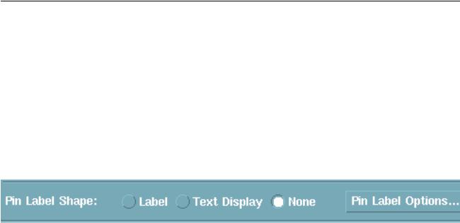
e.To generate name labels for each design element, turn on Pin Label Shape – Label. (You must first turn on theDisplay Pin Name option on the form associated with the layout editor Create – Pin command.)
f.To set the style of the pin labels, click Pin Label Options
December 2002 |
165 |
Product Version 5.0 |
Virtuoso XL Layout Editor User Guide
Generating Your Layout with Virtuoso XL Layout Editor
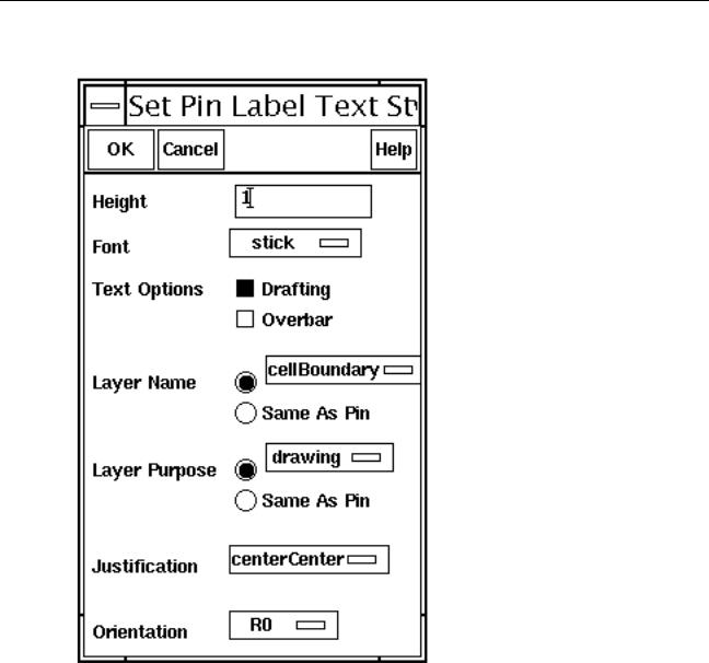
The Set Pin Label Text Style form appears.
g. Choose the options you want from the Set Pin Label Text Style form and click OK.
December 2002 |
166 |
Product Version 5.0 |
Virtuoso XL Layout Editor User Guide
Generating Your Layout with Virtuoso XL Layout Editor
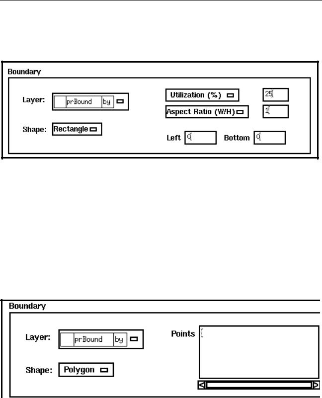
4.In the Boundary section of the Layout Generation Options form, if you want Virtuoso XL to draw a boundary, follow these steps.
a.In the Layer field, choose the layer you want to use for the boundary.
b.In the Shape field, chooseRectangle or Polygon.
To specify the dimensions of a rectangular boundary, you can use only two of the following four values: Utilization (%), Aspect Ratio (Width/Height), Boundary
Width, or Boundary Height. You can also type in the Points field values for the Left (Y coordinate) side of the boundary and the Bottom (X coordinate) side of the boundary in this format: (0 0) (10 10).
To specify the dimensions of a polygonal boundary, choose Polygon from the Shape field and type the X and Y coordinates of each corner of the polygon in the Points field in the following format. For example, for a rectangle, type:(0 0) (0 10) (10 8) (8 0) (0 0).
December 2002 |
167 |
Product Version 5.0 |
Virtuoso XL Layout Editor User Guide
Generating Your Layout with Virtuoso XL Layout Editor
When you move the cursor in the layout window, the X and Y coordinates of the location of the cursor are displayed in the Status Line at the top of the layout window.
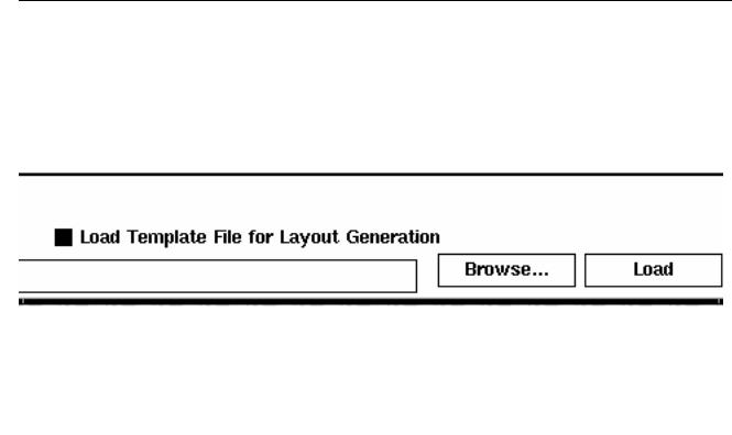
5.In the Template File section, to load a template file (an ASCII file containing the information entered in this form in a previous session and saved to a file), follow these steps.
a.Select the Load Template File for Layout Generation option.
b.Click Browse.
You can set an environment variable, templateFileName, to always load the name of a template you specify as the value of the variable.
December 2002 |
168 |
Product Version 5.0 |
Virtuoso XL Layout Editor User Guide
Generating Your Layout with Virtuoso XL Layout Editor
The Open File form appears.
c.Click on the directories in the left list box to descend into your file hierarchy until you reach the name of the template file to use.
d.Click on the name of the template file in the right list box to enter it in theName field.
The left and right arrows at the right side of the form let you go up and down in the file hierarchy.
e.Click OK.
The file name is displayed in the text field at the bottom of the Layout Generation
Options form.
December 2002 |
169 |
Product Version 5.0 |
Virtuoso XL Layout Editor User Guide
Generating Your Layout with Virtuoso XL Layout Editor
f. Select Load to load the template file.
Caution |
The pin list is refreshed with the pin information from the template file. If there is no pin information saved in a template file from a previous session, then the pin list will be empty. To update the pin list invoke the Connectivity-Update-Components and Nets command.
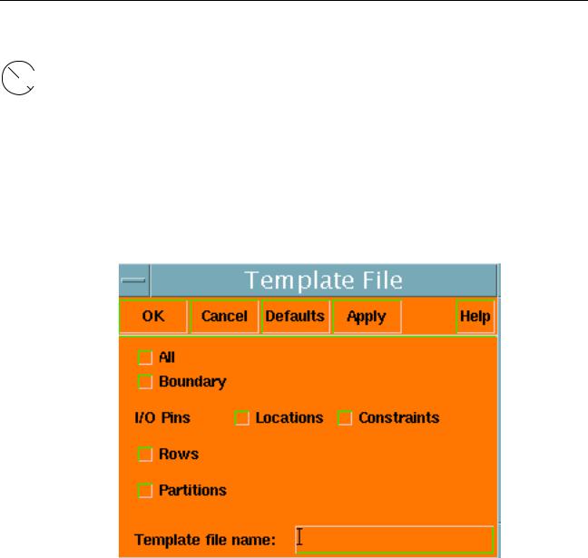
6.To save the template file information stored in the cellview to an ASCII file selectDesignSave To Template.
The Template File form appears.
7.In the Template File form turn on Boundary and I/O Pins.
8.In the Template file name text field specify a user-defined template file name.
9.Click OK.
Note: When you use the Gen From Source command, constraints entered for layout devices are preserved. When you use the Virtuoso layout editor commands Design –
Discard Edits and Design – Open, however, constraints entered for layout devices are lost unless you first save all changes made to the design.
December 2002 |
170 |
Product Version 5.0 |
Virtuoso XL Layout Editor User Guide
Generating Your Layout with Virtuoso XL Layout Editor
Caution |
Before you click OK in the Layout Generation Options form, remember that clicking OK in this form deletes everything in the layout window.
10.Click OK in the Layout Generation Options form.
If you already have design elements in the layout window, a message box warns you that this command deletes all layout instances and wiring in the design.
11.Click Yes on the message box.
Virtuoso XL places the device equivalents of the schematic symbols and the pin equivalents of the schematic terminals below the new design boundary.
Virtuoso XL uses a compact placement for the design elements that corresponds to the schematic placement.
If there are no layout instances for components in the schematic, the missing components are reported in a Virtuoso XL Info text window.
Note: If you do not have layout pins for global nets in the schematic and you want to create these pins in the layout, set the initGlobalNetPins environment variable to t in your
.cdsenv file before you start Virtuoso XL.
Note: If you are using inherited connections in your design to assign more than one value to a global net, remember that the netSet properties on schematic instances, which specify the new value of a global signal, are not copied over with the instance from the schematic to the layout when you use the Gen From Source, Pick from Schematic, or Update Layout Parameters command.
Note: If you are using inherited connections, the netExpression pin properties which have not been se are copied to the layout terminals. If multiple netExpression properties exist for the same terminal name, then you will be prompted to select at most one property to be preserved on the terminal.
Mismatched Pins
If a symbol in a schematic has more pins than the corresponding device on the layout, Virtuoso XL generates a warning about mismatched pins.
If you want Virtuoso XL to ignore a pin on an instance in the schematic during layout and not generate a warning about mismatched pins for it, follow these steps.
1.Descend into the symbol of the instance and add a Boolean property, named whatever you choose (for example, unusedPin) and set to t, on the pin.
December 2002 |
171 |
Product Version 5.0 |
Virtuoso XL Layout Editor User Guide
Generating Your Layout with Virtuoso XL Layout Editor
2.Add that property name (for example, unusedPin) as a value in the ignoreNames environmental variable in your .cdsenv file
layoutXL ignoreNames string "unusedPin"
or you can type it in the CIW
envSetVal("layoutXL" "ignoreNames" 'string "unusedPin")
The software will not issue a warning of pin mismatches or missing pins during layout generation or when you run the Check – Against Source or Update – Components and Nets command.
Placing Components in a Layout in the Same Relative Position as in the Schematic (Place As In Schematic)
To place all components (or all components you select) inside the design boundary of the layout window in the same relative position as they are in the schematic, follow these steps.
From the layout window, choose Edit – Place As In Schematic.
Virtuoso XL automatically moves all the components into the design boundary according to the relative locations of the symbols in the schematic.
Place As In Schematic will move all components or, in case a selected set exists, only the components in the selected set.
Note: Place As In Schematic does not attempt to fit all the components into the prBoundary. If the schematic is hierarchical or is sparsely drawn, then some or all of the components will be placed outside the boundary.
Place As In Schematic will arrange mFactor devices in a row when the mFactor objects are not abutted together. Iterated instances will be placed in a column when not abutted together.
If some objects in the design, such as pins, are much smaller in size than other objects, such as components, the small objects might not appear in the layout, even though they have been moved. You need to zoom in to see these smaller objects.
If there is no design boundary, Virtuoso XL places the devices within a square the size of the default boundary (25% utilization).
I/O pins will not move. To move the I/O pins so that they align to the edges of the design boundary use the Placer – Pin Placement command.
December 2002 |
172 |
Product Version 5.0 |