

- •Contents
- •Preface
- •Related Documents
- •Typographic and Syntax Conventions
- •Introduction to the Virtuoso XL Layout Editor
- •Editing Your Technology File for Virtuoso XL Layout Editor
- •Sample Technology File
- •Virtuoso XL Technology File Requirements
- •Layer Rules
- •Devices
- •Physical Rules
- •Virtuoso XL Rules (lxRules)
- •Compactor Rules
- •Preparing Your Connectivity Source for the Virtuoso XL Layout Editor
- •Placing Design Elements
- •Using Design Variables
- •Netlist Processor Expressions
- •Analog Expression Language Expressions
- •Simulation Design Variables
- •Using One-to-Many Mapping
- •Iterated Instances and Bus Pins
- •Multiplication Factor (mfactor)
- •Series-Connection Factor (sfactor)
- •One-to-Many Assignment with the Update Device Correspondence
- •Using Many-to-Many or Many-to-One Mapping
- •Modifying Many-to-Many or Many-to-One Mapping Between Components
- •Deleting Many-to-Many or Many-to-One Mapping Between Components
- •Using Virtuoso XL Properties
- •Using the lxUseCell Property to Specify Layout Devices to Use
- •Using the lvsIgnore Property to Exclude Schematic Symbols
- •Using the lxlgnoredParams Property to Exclude Device Properties
- •Using the lxRemoveDevice property to Ignore Parasitic Devices
- •Using the lxViewList and lxStopList Properties to Prepare Hierarchical Designs
- •Using the lxCombination Property to Build Complex Devices
- •Preparing Instances and Pins in Your Layout for the Virtuoso XL Layout Editor
- •Preparing Pins for the Virtuoso XL Layout Editor
- •Preparing Pins for Permutability
- •Search Order Variable
- •Syntax
- •Macros
- •Setting the permuteRule Property in the Symbol Master
- •Setting the permuteRule Property in the Device Master
- •Setting the permuteRule Property in the Symbol Instance
- •Setting the permuteRule Property in the Device Instance
- •Setting the permuteRule Property in the Component Description Format
- •Preparing Instances for Hierarchical Connectivity Checking
- •Setting Up Your Desktop
- •Customizing Your Desktop Layout
- •Using Multiple Cellviews
- •Printing to the Command Interpreter Window
- •Changing Display Colors
- •Using Bindkeys
- •Displaying Bindkeys
- •Loading Virtuoso XL Bindkeys
- •Setting Environment Variables
- •Information About Online Forms
- •Layout XL Options Form
- •Introduction to Abutment
- •Abutment Requirements
- •Setting Up Cells for Abutment
- •abutAccessDir
- •abutClass
- •Steps in Auto-Abutment
- •Sample Parameterized Cells Set Up for Abutment
- •Example 1
- •Example 2
- •Creating CMOS Pcells to Use with Abutment
- •autoAbutment Properties
- •The abutMosStretchMat Property
- •abutMosStretchMat Rules for MOS Abutment
- •Example Code Setting MOS Abutment Properties
- •Setting Environment Variables for Abutment
- •Move Together
- •Constraint Assisted
- •Using Device Abutment
- •Generating Your Layout with Virtuoso XL Layout Editor
- •Starting Virtuoso XL from the Schematic
- •Importing a Netlist for a Connectivity Reference
- •Starting Virtuoso XL from the Layout View
- •Connectivity Reference as a Netlist
- •Mapping File Structure
- •Working with Template Files
- •Saving Form Contents
- •Loading Template Files
- •Modifying Templates
- •Loading Template Files
- •Creating Template Files
- •Template File Syntax
- •General Syntax Rules
- •Boundaries Section
- •I/O Pins Section
- •Sample Template
- •Generating a Layout with Components Not Placed (Gen From Source)
- •Moving Components from the Schematic into the Layout (Pick from Schematic)
- •Placing a Group of Schematic Elements Together
- •Placing Individual Components
- •Generating Pins
- •Viewing Unplaced Instances/Pins
- •Viewing in Place
- •Manually Abutting Devices Using Pick from Schematic
- •Cloning Components
- •Cloning
- •Troubleshooting
- •Cloning Using Multiple Cellviews
- •Using Correspondence Points
- •Information About Online Forms
- •Add Correspondence Pairs Form
- •Cloning Form
- •Correspondence Pairs Form
- •Import XL Netlist Form
- •Layout Generation Options Form
- •Open File Form
- •Pick from Schematic Form
- •Remove Correspondence Components Form
- •Set Pin Label Text Style Form
- •Startup Option Form
- •Template File Form
- •Editing Your Layout with Virtuoso XL Layout Editor
- •Identifying Incomplete Nets
- •Moving Objects Manually in the Virtuoso XL Layout Editor
- •Moving Objects Using Move Options
- •Setting the Move Form to Appear Automatically
- •Aligning Objects
- •Post Selecting Devices
- •PreSelecting Devices
- •Swapping Components
- •Permuting Component Pins
- •Permuting Pins Manually
- •Checking Permutation Information
- •Using Device Locking
- •Using Automatic Spacing
- •Using Interactive Device Abutment
- •Setting Component Types
- •About Component Types
- •MOS Transistor Stacking and Folding Parameters
- •Modifying a Component Type
- •Using Transistor Chaining
- •Using Transistor Folding
- •Controlling the Folding Grid
- •Folding Transistors
- •Adding Instances to a Layout
- •Adding Pins to a Layout
- •Assigning Pins to a Net
- •Maintaining Connectivity When Editing a Flattened Pcell
- •Information About Online Forms
- •Assign Nets Form
- •Edit Component Types Form
- •Move Form
- •Set Transistor Folding Form
- •Show Incomplete Nets Form
- •Stretch Form
- •Virtuoso XL Alignment Form
- •Using the Virtuoso Custom Placer
- •Overview
- •Main Features
- •Place Menu Command Summary
- •Other Commands Used with the Virtuoso custom placer
- •Placement Styles
- •Setting Up the Virtuoso XL Layout Editor for Placement
- •Identifying the Placement Translation Rules
- •Setting Cadence Design Framework II Environment Variables
- •Setting Environment Variables for the Virtuoso Custom Router and Placer
- •Setting MOS Chaining and Folding Parameters
- •Abutting Standard Cells
- •Using Auto-Abutment During Placement
- •Placement Constraints
- •Constraint Manager Geometric Constraints
- •Pin Placement Constraints
- •Constraint Limitations
- •Placement Parameters and Component Types
- •MOS Transistor Chaining and Folding Parameters
- •Pin Placement
- •Assigning Pins to an Edge
- •Assigning Pins to a Fixed Position
- •Railing Pins
- •Loading the Template File
- •Assigning Spacing Between Pins
- •Saving Pin Placement to a Template File
- •Partitioning the Design
- •Creating a Partition
- •Loading the Template File
- •Saving Partitions to a Template File
- •Setting Placement Planning
- •Assisted CMOS Placement
- •Choose Component Types Form
- •Running the Virtuoso Custom Placer
- •Prerequisites to Placement
- •Running the Virtuoso Custom Placer: Initial Placement
- •Stopping the Placer
- •Running Load Balancing Service (LBS)
- •Troubleshooting Placement Results
- •Running the Virtuoso Custom Placer: Detailed Placement
- •Showing Congestions
- •Information About Forms
- •Auto Placer Form
- •Partitioning Form
- •Choose Component Types Form
- •Pin Placement Form
- •Load Template File Form
- •Placement Planning Form (Assisted CMOS)
- •Placement Planning Form (Assisted Standard Cell)
- •Placement Planning Form (Assisted Mixed CMOS/Standard-Cell)
- •Preparing Your Design for Routing in the Virtuoso XL Layout Editor
- •Understanding Connectivity
- •Pseudo-Parallel Connections
- •Selecting Layers
- •Changing Layers
- •Connecting Nets
- •Creating Paths
- •Connecting Nets with Path Stitching
- •Connecting Nets with Design Shapes
- •Checking Connectivity with Flight Lines
- •Checking Connectivity with Markers
- •Finding Markers
- •Explaining Markers
- •Deleting Single Markers
- •Deleting All Markers
- •Using the Virtuoso Compactor on a Routed Design
- •Overview
- •Main Features
- •Wire Editing Commands
- •Virtuoso Custom Router to Virtuoso XL Command Mapping
- •Prerequisites
- •Rule Information
- •Net Connectivity Information
- •Routing Area Boundary
- •Enabling Wire Editing
- •Toggling Between Virtuoso XL and Wire Editing Enabled
- •Loading ASCII Rules Files
- •The Wire Editing Environment
- •Status Banner
- •Preview Wires and Routing Aids
- •Mouse Button Behavior
- •Using Environment Variables
- •Routing Paths
- •Routing a Single Path
- •Routing Multiple Paths
- •Preventing and Checking Design Rule Violations
- •Interactive Checking
- •Same Net Checking
- •Checking Regions
- •Checking Route and Pin Violations
- •Routing Options and Styles
- •Matching Path Width and Pin Widths
- •Matching Path Width and Pin Widths for Multiple Paths
- •Gathering Bus Wires
- •Spacing for Gathered Bus Wires
- •Overriding Bus Spacing
- •Rotating the Bus Cursor
- •Cycling the Control Wire
- •Allowing Redundant Wiring
- •Allowing Orthogonal Jogs
- •Route To Cursor
- •Allow Floating Nets
- •Connecting Multiple Component Pins
- •Pushing Routes and Components
- •Routing Shielded Nets
- •Routing Tandem Layer Pairs
- •Using Vias
- •Changing Layers and Adding Vias
- •Using Vias Patterns on Multiple Paths
- •Legal Via Sites
- •Rotating Vias
- •Pseudo Vias
- •Editing Routed Connections
- •Stretching Paths and Vias
- •Splitting and Stretching Paths
- •Copying Routes
- •Using Critic Wire
- •Compacting Paths Using Pull
- •Displaying Reports
- •Displaying Routing Status Reports
- •Displaying Network Reports
- •Displaying Component Reports
- •Displaying Net Reports
- •Creating Rules Reports
- •Search Reports
- •Saving Reports
- •Setting Constraints
- •Using the Virtuoso Constraint Manager
- •Using .do Files
- •About the Forms
- •Add Via Form
- •Check Routes Form
- •Create Path Form
- •Find File Form
- •Layout
- •Reports Form
- •Route Options Form
- •Save As Form
- •Search Form
- •Split Form
- •Via Pattern Pop-up
- •Reports
- •Route Status Report Window
- •Network Report Window
- •Instance Report Window
- •Net Report Window
- •Rules Report Window
- •Setting Environment Variables
- •Troubleshooting
- •Finding Design Elements (Probing)
- •Probing Hierarchical Designs
- •Removing Probes
- •Exiting the Probe Command
- •Showing the Options Form
- •Checking Shorts and Opens
- •Comparing Design Elements and Parameters (Checking against the Connectivity Source)
- •Information About Online Forms
- •Probe Options Form
- •Updating Design Data in Virtuoso XL
- •Updating Layout Parameters
- •Updating Schematic Parameters
- •Updating Device Correspondence
- •Creating Device Correspondence
- •Needed Mode
- •Computer Aided Mode
- •Updating the Connectivity Reference
- •Changing the Device (Instance) View
- •Information About Online Forms
- •Change Instance View Form
- •Create Device Correspondence
- •Problems with the Interface
- •Invalid Markers from Previous Software Versions
- •Options Form Does Not Appear
- •Virtuoso XL Performance Is Slow
- •Problems with Editing
- •Components Move Slowly
- •Extra Probes Appear
- •Layout Generation Options Form Does Not Keep Values from the Last Entry
- •Parameters Not Updated
- •Schematic Not Editable
- •Warning to Update Your Design Appears at Startup
- •Problems with Connectivity
- •Connections Not Made
- •Incomplete Nets Command Does Not Recognize Connected Pins and Nets
- •Markers for Nonexistent Overlaps and Shorts Appear
- •Path Ends Not Accepted
- •Placement and Routing Do Not Run
- •Virtuoso XL Does Not Recognize Physical Vias
- •Moving Software Executables To a New Location
- •Environment Variables
- •Virtuoso XL Layout Editor
- •alignApplySeparation
- •alignApplySpacings
- •alignDirection
- •alignLayer
- •alignMethod
- •alignSelectionMode
- •alignSeparation
- •allowRotation
- •autoAbutment
- •autoArrange
- •autoPermutePins
- •autoSpace
- •checkTimeStamps
- •ciwWindow
- •compTypeRefLibs
- •constraintAssistedMode
- •createBoundaryLabel
- •crossSelect
- •extractEnable
- •extractStopLevel
- •globalPlacement
- •ignoredParams
- •ignoreNames
- •incNetCycleHilite
- •incNetHiliteLayer
- •infoWindow
- •initAspectRatio
- •initAspectRatioOption
- •initBoundaryLayer
- •initCreateBoundary
- •initCreateInstances
- •initCreateMTM
- •initCreatePins
- •initDoFolding
- •initDoStacking
- •initEstimateArea
- •initGlobalNetPins
- •initIOLabelType
- •initIOPinLayer
- •initIOPinName
- •initPinHeight
- •initPinMultiplicity
- •initPinWidth
- •initPrBoundaryH
- •initPrBoundaryW
- •initSymbolicPins
- •initUtilization
- •layoutWindow
- •lswWindow
- •lxAllowPseudoParallelNets
- •lxDeltaWidth
- •lxFingeringNames
- •lxGenerationOrientation
- •lxGenerationTopLevelOnly
- •lxInitResetSource
- •lxStackMinimalFolding
- •lxStackPartitionParameters
- •lxWidthTolerance
- •maintainConnections
- •mfactorNames
- •mfactorSplit
- •moveAsGroup
- •openWindow
- •optimizePlacement
- •paramTolerance
- •pathProbe
- •pathPurposeList
- •pathSwitchLayer
- •pathSwitchPurpose
- •preserveTerminalContacts
- •probeCycleHilite
- •probeDevice
- •probeHiliteLayer
- •probeInfoInCIW
- •probeNet
- •probePin
- •rowGroundLayer
- •rowGroundName
- •rowGroundWidth
- •rowPowerLayer
- •rowPowerName
- •rowPowerWidth
- •rowSupplyPosition
- •rowSupplySpacing
- •rowMOSSupplyPattern
- •rowSTDAllowFlip
- •rowSTDSupplyPattern
- •rulesFile
- •runTime
- •saveAs
- •saveAsCellName
- •saveAsLibName
- •saveAsViewName
- •schematicWindow
- •setPPConn
- •sfactorNames
- •sfactorParam
- •showIncNetEnable
- •stopList
- •templateFileName
- •traverseMixedHierarchies
- •updateReplacesMasters
- •updateWithMarkers
- •vcpConductorDepth
- •vcpKeepoutDepth
- •viewList
- •Wire Editor
- •allowFloatingNets
- •allowJogs
- •allowRedundantWiring
- •autoAdjustLength
- •autoShield
- •busOverride
- •busOverrideValue
- •busWireSpacing
- •busWireSpacingType
- •checkCornerCorner
- •checkCrosstalk
- •checkLength
- •checkLimitWay
- •checkMaxProcessWireWidth
- •checkMaxStackViaDepth
- •checkMaxTotalVia
- •checkMinMaskEdgeLength
- •checkMinProcessWireWidth
- •checkMiter
- •checkNetOrder
- •checkOffManGridPin
- •checkOffWireGridPin
- •checkPinSpacing
- •checkPolygonWire
- •checkProtected
- •checkReentrantPath
- •checkRegion
- •checkSameNet
- •checkSegment
- •checkStub
- •checkUseLayers
- •checkUseVias
- •checkWireExtension
- •doFile
- •enableBusRouting
- •enableTandemPair
- •gatherBusWires
- •inaccessiblePin
- •interactiveChecking
- •matchPinWidth
- •matchPinWidthValue
- •matchWireWidth
- •multiplePinsConnection
- •pinLargerMaxProcessWidth
- •pinSmallerMinProcessWidth
- •pushComponent
- •pushRouting
- •routeAsManyAsPossible
- •routeToCursor
- •routeToCursorStyle
- •sameNetChecking
- •showTimingMeter
- •showTimingOctagon
- •snapToPinOrigin
- •useDoFile
- •useRulesFile
- •viaAssistance
- •viaPattern
- •Private Environment Variables
- •Virtuoso XL Command Quick Reference
- •Using Spice and CDL For Netlist Driven Layout Generation
- •Introduction
- •Specifying Spice Designs
- •Cell Creation Rules
- •Character Considerations
- •Spice Statements
- •File Level Statements
- •Statements Allowed at File Level or within a Subckt Cell or a Top Level Cell
- •Statements Allowed within a Subckt Cell or a Top Level Cell
- •Spice Design Example
- •CDL Design Example
- •Parameter Resolution
- •Parameter Levels
- •Resolving Parameters
- •Putting the Rules Together (Examples)
- •Parameter Scaling
- •Complete ibuf Example Results
- •Virtuoso XL .do File Commands
- •Rule Hierarchy
- •circuit
- •Syntax
- •Example
- •Syntax
- •Example
- •limit
- •Syntax
- •Example
- •rule
- •Syntax
- •Example
- •Syntax

Virtuoso XL Layout Editor User Guide
13
Updating Design Data in Virtuoso XL
This chapter explains how to use the Virtuoso® XL layout editor (Virtuoso XL) to make design changes and update your design as you progress. This chapter contains information about the following areas:
■Updating Components and Nets (Engineering Change Order Mode) on page 456
■Updating Layout Parameters on page 461
■Updating Schematic Parameters on page 463
■Updating Device Correspondence on page 465
■Updating the Connectivity Reference on page 472
■Changing the Device (Instance) View on page 473
Information about Virtuoso XL online forms is at the end of the chapter.
December 2002 |
455 |
Product Version 5.0 |

Virtuoso XL Layout Editor User Guide
Updating Design Data in Virtuoso XL
Updating Components and Nets
(Engineering Change Order Mode)
You can automatically update the layout to add any devices, pins, or connectivity changes you have added to the schematic. This operation is sometimes known as Engineering Change
Order (ECO) mode.
It is helpful to have Show Incomplete Nets active when you update components and nets so that you can see that the connectivity you want is made.
To update the components and nets in a layout with changes made to the schematic, follow these steps.
1.Extract the schematic by choosing from the schematic window
Check – Current Cellview.
The schematic editor extracts the connectivity of the design and reports the results in a Schematic Check information window.
2.From the layout window, choose Connectivity – Update – Components and Nets.
Virtuoso XL checks the components and nets in the schematic against the ones in the layout.
If the schematic has changed a Virtuoso XL a dialog box appears indicating that schematic extraction is needed to continue. If you click OK in the dialog box, then Virtuoso XL extracts the schematic hierarchically including the reference libraries. However, the extracted cellviews are not automatically saved.
If you want a different extraction behavious click Cancel in the dialog box and invoke the CheckHierarchy command in the schematic window.
If there are no differences, a message appears in the Command Interpreter Window
(CIW) saying that the check has been completed successfully. If there are differences, the differences are displayed in the CIW.
If devices are found in the layout that are not in the schematic, they are displayed with markers.
If devices or pins in the schematic are missing from the layout, the Layout Generation
Options form opens. For more information about using this form, see the Layout Generation Options Form on page 196.
December 2002 |
456 |
Product Version 5.0 |
Virtuoso XL Layout Editor User Guide
Updating Design Data in Virtuoso XL
If the I/O Pins option is turned on, the pins shown in the I/O Pins section of the form are those that exist in the schematic but are missing from the layout.
Note: the Layout Generation Options form always reflects the default settings for the design; that is, the state of the schematic, not the entries from the previous time the form was used.
3. In the Layout Generation section at the top of the form,
a. If you want to generate pins, instances, or a boundary as specified in the schematic or in a template file, check that the options you want are turned on.
Note: Update Components and Nets only chains or folds new devices after running the Layout Generation Options with chaining and folding. New chains are separate and do not attach to old chains. Devices that had been chained previously to running Update Components and Nets are not moved from their existing positions.
Recreate the abutment into stacks of MOS transistors or fingers of folded MOS transistors that were unabutted since you created them with the Design-Gen From
Source command
December 2002 |
457 |
Product Version 5.0 |

Virtuoso XL Layout Editor User Guide
Updating Design Data in Virtuoso XL
Recreate and fold MOS transistors that were unfolded or all fingers of which were deleted since you created them with the Design – Gen From Source command
If the Transistor Chaining and Transistor Folding options are off, and you have deleted all the fingers of a folded transistor,Update Components and Nets generates a single device. If you have deleted some of the fingers of a folded device, it creates markers only if fingers in a numbered sequence are missing; otherwise it does nothing about missing fingers of folded transistors.
Note:
b.If you want to preserve existing many-to-many mapping of devices between the connectivity source and the layout, turn on Preserve Mappings.
Note: The Preserve Mappings functionality does not report missing devices or shapes within a mapped group.
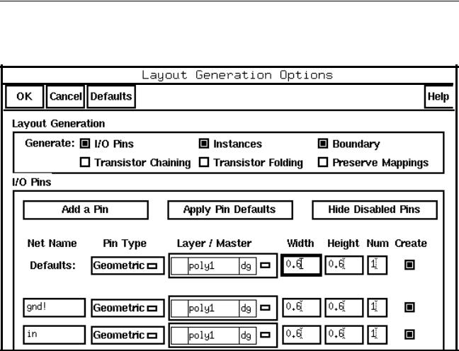
4.For each pin you want to add, click Add a Pin.
An empty pin row opens.
5.For each pin you want to add in the new pin row
a.In the Net Name column, type in a net name.
b.In the Pin Type cyclic field, choose a pin type.
c.In the Layer/Master cyclic field, choose a layer.
d.In the Width field, specify the pin width.
e.In the Height field, specify the pin height.
f.In the Num field, specify the number of pins you want.
6.For all pins set the Pin Label Shape.
a.Set Label to generate labels for each pin on the text dg layer purpose pair.
b.Set Text Display to generate text for each pin on the text dg layer purpose pair.
To view the text, set the Pin Names option on in the Display Options form.
c.Set None to not generate labels for pins.
7.To set the style of the pin labels, click Display Pin Name Option....
The Display Pin Name Option form appears.
December 2002 |
458 |
Product Version 5.0 |
Virtuoso XL Layout Editor User Guide
Updating Design Data in Virtuoso XL
8.Choose the options you want from the Set Pin Label Text Style form and click OK.
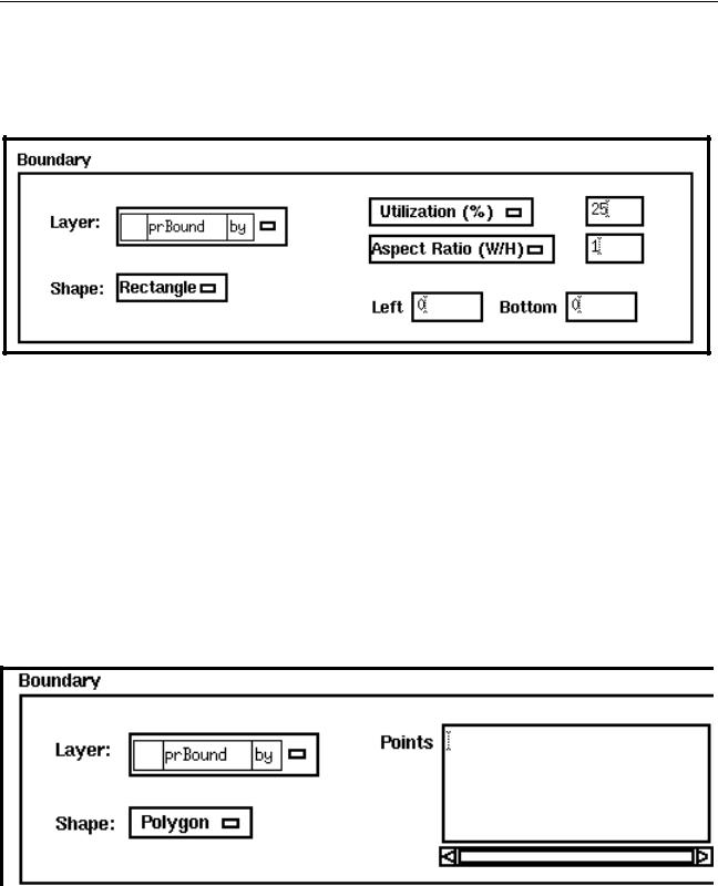
9.In the Boundary section of the Layout Generation Options form, if you want Virtuoso XL to draw a boundary, follow these steps.
a.In the Layer field, choose the layer you want to use for the boundary.
b.In the Shape field, chooseRectangle or Polygon.
To specify the dimensions of a rectangular boundary, you can use only two of the following four values: Utilization %, Aspect Ratio (Width/Height), Boundary Width, or Boundary Height. You can also type in the Points field values for the Left (X coordinate) side of the boundary and the Bottom (Y coordinate) side of the boundary in this format: (0 0) (10 10).
To specify the dimensions of a polygonal boundary, choose Polygon from the Shape field and enter the X and Y coordinates of each angle of the polygon in the Points type-in field in the following format. For example, for a rectangle:0( 0) (0 10)
(10 8) (8 0) (0 0)
December 2002 |
459 |
Product Version 5.0 |
Virtuoso XL Layout Editor User Guide
Updating Design Data in Virtuoso XL
When you move the cursor in the layout window, the X and Y coordinates of the location of the cursor are displayed in the Status Line at the top of the layout window.
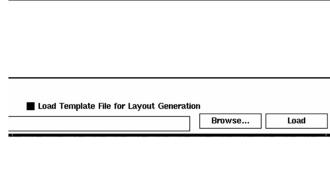
10.In the Template File section, to load a template file, (an ASCII file containing the information entered in this form in a previous session and saved to a file) follow these steps.
a.Select the Load Template File for Layout Generation option.
b.Click the Browse button and the Open File form appears.
c.Click on the directories in the left list box to descend into your file hierarchy until you reach the name of the template file to use.
d.Click on the name of the template file in the right list box to enter it in theName field.
The left and right arrows at the right side of the form let you go up and down in the file hierarchy.
e.Click OK in the Open File form.
The values in the template file are loaded into the Layout Generation Options form and are used during the design session.
You can set an environment variable, templateFileName, to always load the name of a template you specify as the value of the variable.
11.To save the information you enter in the Layout Generation Options form from the cellview to a template file (an ASCII file) to use in a later session., follow these steps.
a.Select Design-Save To Template. The Template File form appears.
b.Turn on the Boundary an I/O Pins options
c.In the Template file name filed type in a template file name
<design_name.lxt>.
d.Click OK.
December 2002 |
460 |
Product Version 5.0 |