- •Contents
- •Preface
- •Related Documents
- •Typographic and Syntax Conventions
- •Introduction to the Virtuoso XL Layout Editor
- •Editing Your Technology File for Virtuoso XL Layout Editor
- •Sample Technology File
- •Virtuoso XL Technology File Requirements
- •Layer Rules
- •Devices
- •Physical Rules
- •Virtuoso XL Rules (lxRules)
- •Compactor Rules
- •Preparing Your Connectivity Source for the Virtuoso XL Layout Editor
- •Placing Design Elements
- •Using Design Variables
- •Netlist Processor Expressions
- •Analog Expression Language Expressions
- •Simulation Design Variables
- •Using One-to-Many Mapping
- •Iterated Instances and Bus Pins
- •Multiplication Factor (mfactor)
- •Series-Connection Factor (sfactor)
- •One-to-Many Assignment with the Update Device Correspondence
- •Using Many-to-Many or Many-to-One Mapping
- •Modifying Many-to-Many or Many-to-One Mapping Between Components
- •Deleting Many-to-Many or Many-to-One Mapping Between Components
- •Using Virtuoso XL Properties
- •Using the lxUseCell Property to Specify Layout Devices to Use
- •Using the lvsIgnore Property to Exclude Schematic Symbols
- •Using the lxlgnoredParams Property to Exclude Device Properties
- •Using the lxRemoveDevice property to Ignore Parasitic Devices
- •Using the lxViewList and lxStopList Properties to Prepare Hierarchical Designs
- •Using the lxCombination Property to Build Complex Devices
- •Preparing Instances and Pins in Your Layout for the Virtuoso XL Layout Editor
- •Preparing Pins for the Virtuoso XL Layout Editor
- •Preparing Pins for Permutability
- •Search Order Variable
- •Syntax
- •Macros
- •Setting the permuteRule Property in the Symbol Master
- •Setting the permuteRule Property in the Device Master
- •Setting the permuteRule Property in the Symbol Instance
- •Setting the permuteRule Property in the Device Instance
- •Setting the permuteRule Property in the Component Description Format
- •Preparing Instances for Hierarchical Connectivity Checking
- •Setting Up Your Desktop
- •Customizing Your Desktop Layout
- •Using Multiple Cellviews
- •Printing to the Command Interpreter Window
- •Changing Display Colors
- •Using Bindkeys
- •Displaying Bindkeys
- •Loading Virtuoso XL Bindkeys
- •Setting Environment Variables
- •Information About Online Forms
- •Layout XL Options Form
- •Introduction to Abutment
- •Abutment Requirements
- •Setting Up Cells for Abutment
- •abutAccessDir
- •abutClass
- •Steps in Auto-Abutment
- •Sample Parameterized Cells Set Up for Abutment
- •Example 1
- •Example 2
- •Creating CMOS Pcells to Use with Abutment
- •autoAbutment Properties
- •The abutMosStretchMat Property
- •abutMosStretchMat Rules for MOS Abutment
- •Example Code Setting MOS Abutment Properties
- •Setting Environment Variables for Abutment
- •Move Together
- •Constraint Assisted
- •Using Device Abutment
- •Generating Your Layout with Virtuoso XL Layout Editor
- •Starting Virtuoso XL from the Schematic
- •Importing a Netlist for a Connectivity Reference
- •Starting Virtuoso XL from the Layout View
- •Connectivity Reference as a Netlist
- •Mapping File Structure
- •Working with Template Files
- •Saving Form Contents
- •Loading Template Files
- •Modifying Templates
- •Loading Template Files
- •Creating Template Files
- •Template File Syntax
- •General Syntax Rules
- •Boundaries Section
- •I/O Pins Section
- •Sample Template
- •Generating a Layout with Components Not Placed (Gen From Source)
- •Moving Components from the Schematic into the Layout (Pick from Schematic)
- •Placing a Group of Schematic Elements Together
- •Placing Individual Components
- •Generating Pins
- •Viewing Unplaced Instances/Pins
- •Viewing in Place
- •Manually Abutting Devices Using Pick from Schematic
- •Cloning Components
- •Cloning
- •Troubleshooting
- •Cloning Using Multiple Cellviews
- •Using Correspondence Points
- •Information About Online Forms
- •Add Correspondence Pairs Form
- •Cloning Form
- •Correspondence Pairs Form
- •Import XL Netlist Form
- •Layout Generation Options Form
- •Open File Form
- •Pick from Schematic Form
- •Remove Correspondence Components Form
- •Set Pin Label Text Style Form
- •Startup Option Form
- •Template File Form
- •Editing Your Layout with Virtuoso XL Layout Editor
- •Identifying Incomplete Nets
- •Moving Objects Manually in the Virtuoso XL Layout Editor
- •Moving Objects Using Move Options
- •Setting the Move Form to Appear Automatically
- •Aligning Objects
- •Post Selecting Devices
- •PreSelecting Devices
- •Swapping Components
- •Permuting Component Pins
- •Permuting Pins Manually
- •Checking Permutation Information
- •Using Device Locking
- •Using Automatic Spacing
- •Using Interactive Device Abutment
- •Setting Component Types
- •About Component Types
- •MOS Transistor Stacking and Folding Parameters
- •Modifying a Component Type
- •Using Transistor Chaining
- •Using Transistor Folding
- •Controlling the Folding Grid
- •Folding Transistors
- •Adding Instances to a Layout
- •Adding Pins to a Layout
- •Assigning Pins to a Net
- •Maintaining Connectivity When Editing a Flattened Pcell
- •Information About Online Forms
- •Assign Nets Form
- •Edit Component Types Form
- •Move Form
- •Set Transistor Folding Form
- •Show Incomplete Nets Form
- •Stretch Form
- •Virtuoso XL Alignment Form
- •Using the Virtuoso Custom Placer
- •Overview
- •Main Features
- •Place Menu Command Summary
- •Other Commands Used with the Virtuoso custom placer
- •Placement Styles
- •Setting Up the Virtuoso XL Layout Editor for Placement
- •Identifying the Placement Translation Rules
- •Setting Cadence Design Framework II Environment Variables
- •Setting Environment Variables for the Virtuoso Custom Router and Placer
- •Setting MOS Chaining and Folding Parameters
- •Abutting Standard Cells
- •Using Auto-Abutment During Placement
- •Placement Constraints
- •Constraint Manager Geometric Constraints
- •Pin Placement Constraints
- •Constraint Limitations
- •Placement Parameters and Component Types
- •MOS Transistor Chaining and Folding Parameters
- •Pin Placement
- •Assigning Pins to an Edge
- •Assigning Pins to a Fixed Position
- •Railing Pins
- •Loading the Template File
- •Assigning Spacing Between Pins
- •Saving Pin Placement to a Template File
- •Partitioning the Design
- •Creating a Partition
- •Loading the Template File
- •Saving Partitions to a Template File
- •Setting Placement Planning
- •Assisted CMOS Placement
- •Choose Component Types Form
- •Running the Virtuoso Custom Placer
- •Prerequisites to Placement
- •Running the Virtuoso Custom Placer: Initial Placement
- •Stopping the Placer
- •Running Load Balancing Service (LBS)
- •Troubleshooting Placement Results
- •Running the Virtuoso Custom Placer: Detailed Placement
- •Showing Congestions
- •Information About Forms
- •Auto Placer Form
- •Partitioning Form
- •Choose Component Types Form
- •Pin Placement Form
- •Load Template File Form
- •Placement Planning Form (Assisted CMOS)
- •Placement Planning Form (Assisted Standard Cell)
- •Placement Planning Form (Assisted Mixed CMOS/Standard-Cell)
- •Preparing Your Design for Routing in the Virtuoso XL Layout Editor
- •Understanding Connectivity
- •Pseudo-Parallel Connections
- •Selecting Layers
- •Changing Layers
- •Connecting Nets
- •Creating Paths
- •Connecting Nets with Path Stitching
- •Connecting Nets with Design Shapes
- •Checking Connectivity with Flight Lines
- •Checking Connectivity with Markers
- •Finding Markers
- •Explaining Markers
- •Deleting Single Markers
- •Deleting All Markers
- •Using the Virtuoso Compactor on a Routed Design
- •Overview
- •Main Features
- •Wire Editing Commands
- •Virtuoso Custom Router to Virtuoso XL Command Mapping
- •Prerequisites
- •Rule Information
- •Net Connectivity Information
- •Routing Area Boundary
- •Enabling Wire Editing
- •Toggling Between Virtuoso XL and Wire Editing Enabled
- •Loading ASCII Rules Files
- •The Wire Editing Environment
- •Status Banner
- •Preview Wires and Routing Aids
- •Mouse Button Behavior
- •Using Environment Variables
- •Routing Paths
- •Routing a Single Path
- •Routing Multiple Paths
- •Preventing and Checking Design Rule Violations
- •Interactive Checking
- •Same Net Checking
- •Checking Regions
- •Checking Route and Pin Violations
- •Routing Options and Styles
- •Matching Path Width and Pin Widths
- •Matching Path Width and Pin Widths for Multiple Paths
- •Gathering Bus Wires
- •Spacing for Gathered Bus Wires
- •Overriding Bus Spacing
- •Rotating the Bus Cursor
- •Cycling the Control Wire
- •Allowing Redundant Wiring
- •Allowing Orthogonal Jogs
- •Route To Cursor
- •Allow Floating Nets
- •Connecting Multiple Component Pins
- •Pushing Routes and Components
- •Routing Shielded Nets
- •Routing Tandem Layer Pairs
- •Using Vias
- •Changing Layers and Adding Vias
- •Using Vias Patterns on Multiple Paths
- •Legal Via Sites
- •Rotating Vias
- •Pseudo Vias
- •Editing Routed Connections
- •Stretching Paths and Vias
- •Splitting and Stretching Paths
- •Copying Routes
- •Using Critic Wire
- •Compacting Paths Using Pull
- •Displaying Reports
- •Displaying Routing Status Reports
- •Displaying Network Reports
- •Displaying Component Reports
- •Displaying Net Reports
- •Creating Rules Reports
- •Search Reports
- •Saving Reports
- •Setting Constraints
- •Using the Virtuoso Constraint Manager
- •Using .do Files
- •About the Forms
- •Add Via Form
- •Check Routes Form
- •Create Path Form
- •Find File Form
- •Layout
- •Reports Form
- •Route Options Form
- •Save As Form
- •Search Form
- •Split Form
- •Via Pattern Pop-up
- •Reports
- •Route Status Report Window
- •Network Report Window
- •Instance Report Window
- •Net Report Window
- •Rules Report Window
- •Setting Environment Variables
- •Troubleshooting
- •Finding Design Elements (Probing)
- •Probing Hierarchical Designs
- •Removing Probes
- •Exiting the Probe Command
- •Showing the Options Form
- •Checking Shorts and Opens
- •Comparing Design Elements and Parameters (Checking against the Connectivity Source)
- •Information About Online Forms
- •Probe Options Form
- •Updating Design Data in Virtuoso XL
- •Updating Layout Parameters
- •Updating Schematic Parameters
- •Updating Device Correspondence
- •Creating Device Correspondence
- •Needed Mode
- •Computer Aided Mode
- •Updating the Connectivity Reference
- •Changing the Device (Instance) View
- •Information About Online Forms
- •Change Instance View Form
- •Create Device Correspondence
- •Problems with the Interface
- •Invalid Markers from Previous Software Versions
- •Options Form Does Not Appear
- •Virtuoso XL Performance Is Slow
- •Problems with Editing
- •Components Move Slowly
- •Extra Probes Appear
- •Layout Generation Options Form Does Not Keep Values from the Last Entry
- •Parameters Not Updated
- •Schematic Not Editable
- •Warning to Update Your Design Appears at Startup
- •Problems with Connectivity
- •Connections Not Made
- •Incomplete Nets Command Does Not Recognize Connected Pins and Nets
- •Markers for Nonexistent Overlaps and Shorts Appear
- •Path Ends Not Accepted
- •Placement and Routing Do Not Run
- •Virtuoso XL Does Not Recognize Physical Vias
- •Moving Software Executables To a New Location
- •Environment Variables
- •Virtuoso XL Layout Editor
- •alignApplySeparation
- •alignApplySpacings
- •alignDirection
- •alignLayer
- •alignMethod
- •alignSelectionMode
- •alignSeparation
- •allowRotation
- •autoAbutment
- •autoArrange
- •autoPermutePins
- •autoSpace
- •checkTimeStamps
- •ciwWindow
- •compTypeRefLibs
- •constraintAssistedMode
- •createBoundaryLabel
- •crossSelect
- •extractEnable
- •extractStopLevel
- •globalPlacement
- •ignoredParams
- •ignoreNames
- •incNetCycleHilite
- •incNetHiliteLayer
- •infoWindow
- •initAspectRatio
- •initAspectRatioOption
- •initBoundaryLayer
- •initCreateBoundary
- •initCreateInstances
- •initCreateMTM
- •initCreatePins
- •initDoFolding
- •initDoStacking
- •initEstimateArea
- •initGlobalNetPins
- •initIOLabelType
- •initIOPinLayer
- •initIOPinName
- •initPinHeight
- •initPinMultiplicity
- •initPinWidth
- •initPrBoundaryH
- •initPrBoundaryW
- •initSymbolicPins
- •initUtilization
- •layoutWindow
- •lswWindow
- •lxAllowPseudoParallelNets
- •lxDeltaWidth
- •lxFingeringNames
- •lxGenerationOrientation
- •lxGenerationTopLevelOnly
- •lxInitResetSource
- •lxStackMinimalFolding
- •lxStackPartitionParameters
- •lxWidthTolerance
- •maintainConnections
- •mfactorNames
- •mfactorSplit
- •moveAsGroup
- •openWindow
- •optimizePlacement
- •paramTolerance
- •pathProbe
- •pathPurposeList
- •pathSwitchLayer
- •pathSwitchPurpose
- •preserveTerminalContacts
- •probeCycleHilite
- •probeDevice
- •probeHiliteLayer
- •probeInfoInCIW
- •probeNet
- •probePin
- •rowGroundLayer
- •rowGroundName
- •rowGroundWidth
- •rowPowerLayer
- •rowPowerName
- •rowPowerWidth
- •rowSupplyPosition
- •rowSupplySpacing
- •rowMOSSupplyPattern
- •rowSTDAllowFlip
- •rowSTDSupplyPattern
- •rulesFile
- •runTime
- •saveAs
- •saveAsCellName
- •saveAsLibName
- •saveAsViewName
- •schematicWindow
- •setPPConn
- •sfactorNames
- •sfactorParam
- •showIncNetEnable
- •stopList
- •templateFileName
- •traverseMixedHierarchies
- •updateReplacesMasters
- •updateWithMarkers
- •vcpConductorDepth
- •vcpKeepoutDepth
- •viewList
- •Wire Editor
- •allowFloatingNets
- •allowJogs
- •allowRedundantWiring
- •autoAdjustLength
- •autoShield
- •busOverride
- •busOverrideValue
- •busWireSpacing
- •busWireSpacingType
- •checkCornerCorner
- •checkCrosstalk
- •checkLength
- •checkLimitWay
- •checkMaxProcessWireWidth
- •checkMaxStackViaDepth
- •checkMaxTotalVia
- •checkMinMaskEdgeLength
- •checkMinProcessWireWidth
- •checkMiter
- •checkNetOrder
- •checkOffManGridPin
- •checkOffWireGridPin
- •checkPinSpacing
- •checkPolygonWire
- •checkProtected
- •checkReentrantPath
- •checkRegion
- •checkSameNet
- •checkSegment
- •checkStub
- •checkUseLayers
- •checkUseVias
- •checkWireExtension
- •doFile
- •enableBusRouting
- •enableTandemPair
- •gatherBusWires
- •inaccessiblePin
- •interactiveChecking
- •matchPinWidth
- •matchPinWidthValue
- •matchWireWidth
- •multiplePinsConnection
- •pinLargerMaxProcessWidth
- •pinSmallerMinProcessWidth
- •pushComponent
- •pushRouting
- •routeAsManyAsPossible
- •routeToCursor
- •routeToCursorStyle
- •sameNetChecking
- •showTimingMeter
- •showTimingOctagon
- •snapToPinOrigin
- •useDoFile
- •useRulesFile
- •viaAssistance
- •viaPattern
- •Private Environment Variables
- •Virtuoso XL Command Quick Reference
- •Using Spice and CDL For Netlist Driven Layout Generation
- •Introduction
- •Specifying Spice Designs
- •Cell Creation Rules
- •Character Considerations
- •Spice Statements
- •File Level Statements
- •Statements Allowed at File Level or within a Subckt Cell or a Top Level Cell
- •Statements Allowed within a Subckt Cell or a Top Level Cell
- •Spice Design Example
- •CDL Design Example
- •Parameter Resolution
- •Parameter Levels
- •Resolving Parameters
- •Putting the Rules Together (Examples)
- •Parameter Scaling
- •Complete ibuf Example Results
- •Virtuoso XL .do File Commands
- •Rule Hierarchy
- •circuit
- •Syntax
- •Example
- •Syntax
- •Example
- •limit
- •Syntax
- •Example
- •rule
- •Syntax
- •Example
- •Syntax
Virtuoso XL Layout Editor User Guide
Setting Up Your Virtuoso XL Layout Editor Environment
environment information to the layout cellview as a property. When you open the layout and schematic cellviews the next time, they appear in the same configuration as they had when you saved them.
The command sends the LSW and the CIW window size and location information to the
.cdsenv file.
To prevent Virtuoso XL from rearranging or resizing windows from the way you have arranged them, add the following line to the .cdsenv file:
envSetVal(“layoutXL” “autoArrange” ‘boolean nil)
Note: If you save your current window positions and form settings to a file other than
.cdsenv (for example, .envFileName), you can recall them by typing the following in the
CIW or in your .cdsinit file:
envLoadFile("layoutXL" ".envFileName")
Using Multiple Cellviews
If you open multiple cellviews in Virtuoso XL, the second and subsequent sets of windows are not automatically configured the way the first set is.
You can open more than one schematic-layout pair of windows in Virtuoso XL and work on each pair independently. If you open a schematic and two copies of the same layout, the Virtuoso XL Connectivity – Check, Connectivity – Probe, and Connectivity – Update commands apply to both layouts.
If you have a schematic and two different layouts open, the Virtuoso XL Connectivity – Check, Connectivity – Probe, and Connectivity – Update commands apply to only the layout from which you selected the command.
Printing to the Command Interpreter Window
To instruct Virtuoso XL to print process information to the CIW, not to a separate Virtuoso XL Info window, type the following command in the CIW or store it in your .cdsenv file:
envSetVal(“layoutXL” “infoWindow” ‘boolean nil)
Changing Display Colors
You can change the colors and characteristics of the entry layers that Virtuoso XL commands use for display purposes. You can change the display layers Virtuoso XL uses for the following commands:
December 2002 |
101 |
Product Version 5.0 |
Virtuoso XL Layout Editor User Guide
Setting Up Your Virtuoso XL Layout Editor Environment
■The Show Incomplete Nets command uses the y0 – y9 entry layers to show flight lines
■The Connectivity – Check – Against Source command uses the hilite drawing9 entry layer to identify missing devices
■The Connectivity – Probe command uses the hilite drawing through hilite drawing9 entry layers to probe pins, nets, and devices
■The Highlight command for placement constraints uses the annotate drawing3 entry layer to highlight in the layout the components bound by a placement constraint
■The Pick from Schematic command uses the hilite drawing1 layer to highlight schematic symbols
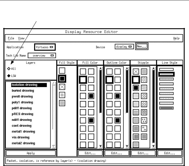
You can edit these layers from the window opened by the CIW Tools – Display Resources
– Editor command.
Note: Although it is possible to edit these layers from the LSW, it is not recommended. To do so, you must add these layers to the LSW as valid layers. Valid layers are those you use for creating layout shapes.
To change the colors using the Display Resources Editor, follow these steps.
1.In the CIW, choose Tools – Display Resources – Editor.
2.In the Display Resources Tool Box select Edit....
December 2002 |
102 |
Product Version 5.0 |
Virtuoso XL Layout Editor User Guide
Setting Up Your Virtuoso XL Layout Editor Environment
The Display Resource Editor window appears.
Click on All
3.Turn on All, so that you can see all of the available layers (not just the ones you have defined as drawing layers).
4.In the Layers column, choose the name of the layer to change.
5.Turn on the Fill Style, Fill Color, Outline Color, Stipple, and Line Style options you want to use for that layer.
6.Click Apply.
The next time you use a command that displays the layer you changed, the color or pattern changes in the design window.
December 2002 |
103 |
Product Version 5.0 |
Virtuoso XL Layout Editor User Guide
Setting Up Your Virtuoso XL Layout Editor Environment
To highlight incomplete connections with flight lines, Virtuoso XL cycles through the y0 – y9 layers.
Unconnected nets
in
|
|
|
npn |
|
npn |
|
npn |
|
|
|
|
|
|||
|
|
|
|
|
|||
|
|
|
|
|
|||
|
|||||||
|
|
|
Virtuoso XL displays the flight lines of each net in a different color. If there are more than 10 incomplete nets, the colors repeat unless you have specified layers for specific nets (see “Incomplete Nets”).
If you assign new colors to the flight lines,
■Assign colors that do not resemble each other or resemble the colors you use for paths and components
■Avoid solid fill so you can see what is underneath
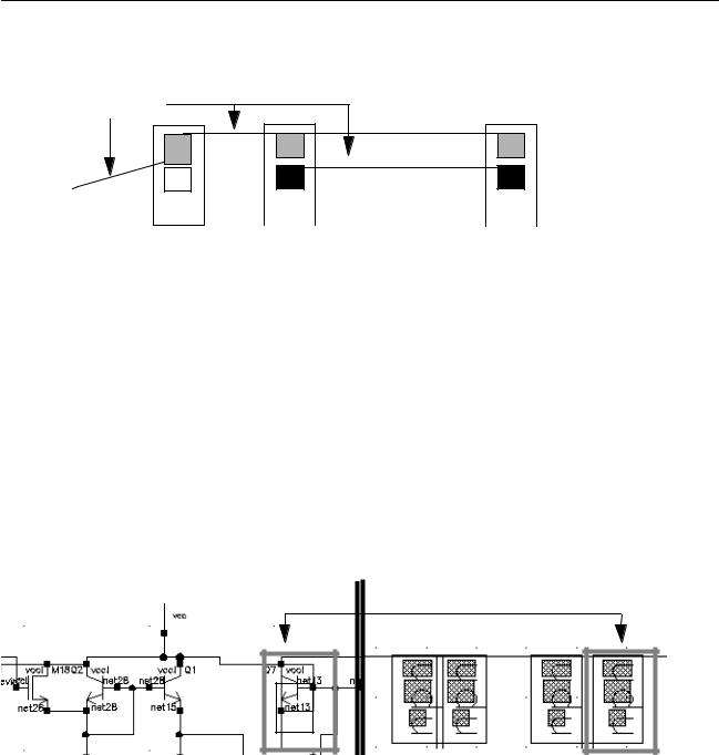
Virtuoso XL uses the hilite drawing through hilite drawing9 entry layers for probes, which identify equivalent design elements on the schematic and the layout.
Schematic |
Layout |
|
Q7 |
Equivalent design elements |
Q7 |
|
Virtuoso XL uses the hilite drawing9 layer to identify components in the schematic that are not in the layout (and vice versa) with the Connectivity – Check – Against Source command.
If you change the colors of the hilite drawing layers,
■Use thick lines so you can see device pins
December 2002 |
104 |
Product Version 5.0 |