- •Contents
- •Preface
- •Related Documents
- •Typographic and Syntax Conventions
- •Introduction to the Virtuoso XL Layout Editor
- •Editing Your Technology File for Virtuoso XL Layout Editor
- •Sample Technology File
- •Virtuoso XL Technology File Requirements
- •Layer Rules
- •Devices
- •Physical Rules
- •Virtuoso XL Rules (lxRules)
- •Compactor Rules
- •Preparing Your Connectivity Source for the Virtuoso XL Layout Editor
- •Placing Design Elements
- •Using Design Variables
- •Netlist Processor Expressions
- •Analog Expression Language Expressions
- •Simulation Design Variables
- •Using One-to-Many Mapping
- •Iterated Instances and Bus Pins
- •Multiplication Factor (mfactor)
- •Series-Connection Factor (sfactor)
- •One-to-Many Assignment with the Update Device Correspondence
- •Using Many-to-Many or Many-to-One Mapping
- •Modifying Many-to-Many or Many-to-One Mapping Between Components
- •Deleting Many-to-Many or Many-to-One Mapping Between Components
- •Using Virtuoso XL Properties
- •Using the lxUseCell Property to Specify Layout Devices to Use
- •Using the lvsIgnore Property to Exclude Schematic Symbols
- •Using the lxlgnoredParams Property to Exclude Device Properties
- •Using the lxRemoveDevice property to Ignore Parasitic Devices
- •Using the lxViewList and lxStopList Properties to Prepare Hierarchical Designs
- •Using the lxCombination Property to Build Complex Devices
- •Preparing Instances and Pins in Your Layout for the Virtuoso XL Layout Editor
- •Preparing Pins for the Virtuoso XL Layout Editor
- •Preparing Pins for Permutability
- •Search Order Variable
- •Syntax
- •Macros
- •Setting the permuteRule Property in the Symbol Master
- •Setting the permuteRule Property in the Device Master
- •Setting the permuteRule Property in the Symbol Instance
- •Setting the permuteRule Property in the Device Instance
- •Setting the permuteRule Property in the Component Description Format
- •Preparing Instances for Hierarchical Connectivity Checking
- •Setting Up Your Desktop
- •Customizing Your Desktop Layout
- •Using Multiple Cellviews
- •Printing to the Command Interpreter Window
- •Changing Display Colors
- •Using Bindkeys
- •Displaying Bindkeys
- •Loading Virtuoso XL Bindkeys
- •Setting Environment Variables
- •Information About Online Forms
- •Layout XL Options Form
- •Introduction to Abutment
- •Abutment Requirements
- •Setting Up Cells for Abutment
- •abutAccessDir
- •abutClass
- •Steps in Auto-Abutment
- •Sample Parameterized Cells Set Up for Abutment
- •Example 1
- •Example 2
- •Creating CMOS Pcells to Use with Abutment
- •autoAbutment Properties
- •The abutMosStretchMat Property
- •abutMosStretchMat Rules for MOS Abutment
- •Example Code Setting MOS Abutment Properties
- •Setting Environment Variables for Abutment
- •Move Together
- •Constraint Assisted
- •Using Device Abutment
- •Generating Your Layout with Virtuoso XL Layout Editor
- •Starting Virtuoso XL from the Schematic
- •Importing a Netlist for a Connectivity Reference
- •Starting Virtuoso XL from the Layout View
- •Connectivity Reference as a Netlist
- •Mapping File Structure
- •Working with Template Files
- •Saving Form Contents
- •Loading Template Files
- •Modifying Templates
- •Loading Template Files
- •Creating Template Files
- •Template File Syntax
- •General Syntax Rules
- •Boundaries Section
- •I/O Pins Section
- •Sample Template
- •Generating a Layout with Components Not Placed (Gen From Source)
- •Moving Components from the Schematic into the Layout (Pick from Schematic)
- •Placing a Group of Schematic Elements Together
- •Placing Individual Components
- •Generating Pins
- •Viewing Unplaced Instances/Pins
- •Viewing in Place
- •Manually Abutting Devices Using Pick from Schematic
- •Cloning Components
- •Cloning
- •Troubleshooting
- •Cloning Using Multiple Cellviews
- •Using Correspondence Points
- •Information About Online Forms
- •Add Correspondence Pairs Form
- •Cloning Form
- •Correspondence Pairs Form
- •Import XL Netlist Form
- •Layout Generation Options Form
- •Open File Form
- •Pick from Schematic Form
- •Remove Correspondence Components Form
- •Set Pin Label Text Style Form
- •Startup Option Form
- •Template File Form
- •Editing Your Layout with Virtuoso XL Layout Editor
- •Identifying Incomplete Nets
- •Moving Objects Manually in the Virtuoso XL Layout Editor
- •Moving Objects Using Move Options
- •Setting the Move Form to Appear Automatically
- •Aligning Objects
- •Post Selecting Devices
- •PreSelecting Devices
- •Swapping Components
- •Permuting Component Pins
- •Permuting Pins Manually
- •Checking Permutation Information
- •Using Device Locking
- •Using Automatic Spacing
- •Using Interactive Device Abutment
- •Setting Component Types
- •About Component Types
- •MOS Transistor Stacking and Folding Parameters
- •Modifying a Component Type
- •Using Transistor Chaining
- •Using Transistor Folding
- •Controlling the Folding Grid
- •Folding Transistors
- •Adding Instances to a Layout
- •Adding Pins to a Layout
- •Assigning Pins to a Net
- •Maintaining Connectivity When Editing a Flattened Pcell
- •Information About Online Forms
- •Assign Nets Form
- •Edit Component Types Form
- •Move Form
- •Set Transistor Folding Form
- •Show Incomplete Nets Form
- •Stretch Form
- •Virtuoso XL Alignment Form
- •Using the Virtuoso Custom Placer
- •Overview
- •Main Features
- •Place Menu Command Summary
- •Other Commands Used with the Virtuoso custom placer
- •Placement Styles
- •Setting Up the Virtuoso XL Layout Editor for Placement
- •Identifying the Placement Translation Rules
- •Setting Cadence Design Framework II Environment Variables
- •Setting Environment Variables for the Virtuoso Custom Router and Placer
- •Setting MOS Chaining and Folding Parameters
- •Abutting Standard Cells
- •Using Auto-Abutment During Placement
- •Placement Constraints
- •Constraint Manager Geometric Constraints
- •Pin Placement Constraints
- •Constraint Limitations
- •Placement Parameters and Component Types
- •MOS Transistor Chaining and Folding Parameters
- •Pin Placement
- •Assigning Pins to an Edge
- •Assigning Pins to a Fixed Position
- •Railing Pins
- •Loading the Template File
- •Assigning Spacing Between Pins
- •Saving Pin Placement to a Template File
- •Partitioning the Design
- •Creating a Partition
- •Loading the Template File
- •Saving Partitions to a Template File
- •Setting Placement Planning
- •Assisted CMOS Placement
- •Choose Component Types Form
- •Running the Virtuoso Custom Placer
- •Prerequisites to Placement
- •Running the Virtuoso Custom Placer: Initial Placement
- •Stopping the Placer
- •Running Load Balancing Service (LBS)
- •Troubleshooting Placement Results
- •Running the Virtuoso Custom Placer: Detailed Placement
- •Showing Congestions
- •Information About Forms
- •Auto Placer Form
- •Partitioning Form
- •Choose Component Types Form
- •Pin Placement Form
- •Load Template File Form
- •Placement Planning Form (Assisted CMOS)
- •Placement Planning Form (Assisted Standard Cell)
- •Placement Planning Form (Assisted Mixed CMOS/Standard-Cell)
- •Preparing Your Design for Routing in the Virtuoso XL Layout Editor
- •Understanding Connectivity
- •Pseudo-Parallel Connections
- •Selecting Layers
- •Changing Layers
- •Connecting Nets
- •Creating Paths
- •Connecting Nets with Path Stitching
- •Connecting Nets with Design Shapes
- •Checking Connectivity with Flight Lines
- •Checking Connectivity with Markers
- •Finding Markers
- •Explaining Markers
- •Deleting Single Markers
- •Deleting All Markers
- •Using the Virtuoso Compactor on a Routed Design
- •Overview
- •Main Features
- •Wire Editing Commands
- •Virtuoso Custom Router to Virtuoso XL Command Mapping
- •Prerequisites
- •Rule Information
- •Net Connectivity Information
- •Routing Area Boundary
- •Enabling Wire Editing
- •Toggling Between Virtuoso XL and Wire Editing Enabled
- •Loading ASCII Rules Files
- •The Wire Editing Environment
- •Status Banner
- •Preview Wires and Routing Aids
- •Mouse Button Behavior
- •Using Environment Variables
- •Routing Paths
- •Routing a Single Path
- •Routing Multiple Paths
- •Preventing and Checking Design Rule Violations
- •Interactive Checking
- •Same Net Checking
- •Checking Regions
- •Checking Route and Pin Violations
- •Routing Options and Styles
- •Matching Path Width and Pin Widths
- •Matching Path Width and Pin Widths for Multiple Paths
- •Gathering Bus Wires
- •Spacing for Gathered Bus Wires
- •Overriding Bus Spacing
- •Rotating the Bus Cursor
- •Cycling the Control Wire
- •Allowing Redundant Wiring
- •Allowing Orthogonal Jogs
- •Route To Cursor
- •Allow Floating Nets
- •Connecting Multiple Component Pins
- •Pushing Routes and Components
- •Routing Shielded Nets
- •Routing Tandem Layer Pairs
- •Using Vias
- •Changing Layers and Adding Vias
- •Using Vias Patterns on Multiple Paths
- •Legal Via Sites
- •Rotating Vias
- •Pseudo Vias
- •Editing Routed Connections
- •Stretching Paths and Vias
- •Splitting and Stretching Paths
- •Copying Routes
- •Using Critic Wire
- •Compacting Paths Using Pull
- •Displaying Reports
- •Displaying Routing Status Reports
- •Displaying Network Reports
- •Displaying Component Reports
- •Displaying Net Reports
- •Creating Rules Reports
- •Search Reports
- •Saving Reports
- •Setting Constraints
- •Using the Virtuoso Constraint Manager
- •Using .do Files
- •About the Forms
- •Add Via Form
- •Check Routes Form
- •Create Path Form
- •Find File Form
- •Layout
- •Reports Form
- •Route Options Form
- •Save As Form
- •Search Form
- •Split Form
- •Via Pattern Pop-up
- •Reports
- •Route Status Report Window
- •Network Report Window
- •Instance Report Window
- •Net Report Window
- •Rules Report Window
- •Setting Environment Variables
- •Troubleshooting
- •Finding Design Elements (Probing)
- •Probing Hierarchical Designs
- •Removing Probes
- •Exiting the Probe Command
- •Showing the Options Form
- •Checking Shorts and Opens
- •Comparing Design Elements and Parameters (Checking against the Connectivity Source)
- •Information About Online Forms
- •Probe Options Form
- •Updating Design Data in Virtuoso XL
- •Updating Layout Parameters
- •Updating Schematic Parameters
- •Updating Device Correspondence
- •Creating Device Correspondence
- •Needed Mode
- •Computer Aided Mode
- •Updating the Connectivity Reference
- •Changing the Device (Instance) View
- •Information About Online Forms
- •Change Instance View Form
- •Create Device Correspondence
- •Problems with the Interface
- •Invalid Markers from Previous Software Versions
- •Options Form Does Not Appear
- •Virtuoso XL Performance Is Slow
- •Problems with Editing
- •Components Move Slowly
- •Extra Probes Appear
- •Layout Generation Options Form Does Not Keep Values from the Last Entry
- •Parameters Not Updated
- •Schematic Not Editable
- •Warning to Update Your Design Appears at Startup
- •Problems with Connectivity
- •Connections Not Made
- •Incomplete Nets Command Does Not Recognize Connected Pins and Nets
- •Markers for Nonexistent Overlaps and Shorts Appear
- •Path Ends Not Accepted
- •Placement and Routing Do Not Run
- •Virtuoso XL Does Not Recognize Physical Vias
- •Moving Software Executables To a New Location
- •Environment Variables
- •Virtuoso XL Layout Editor
- •alignApplySeparation
- •alignApplySpacings
- •alignDirection
- •alignLayer
- •alignMethod
- •alignSelectionMode
- •alignSeparation
- •allowRotation
- •autoAbutment
- •autoArrange
- •autoPermutePins
- •autoSpace
- •checkTimeStamps
- •ciwWindow
- •compTypeRefLibs
- •constraintAssistedMode
- •createBoundaryLabel
- •crossSelect
- •extractEnable
- •extractStopLevel
- •globalPlacement
- •ignoredParams
- •ignoreNames
- •incNetCycleHilite
- •incNetHiliteLayer
- •infoWindow
- •initAspectRatio
- •initAspectRatioOption
- •initBoundaryLayer
- •initCreateBoundary
- •initCreateInstances
- •initCreateMTM
- •initCreatePins
- •initDoFolding
- •initDoStacking
- •initEstimateArea
- •initGlobalNetPins
- •initIOLabelType
- •initIOPinLayer
- •initIOPinName
- •initPinHeight
- •initPinMultiplicity
- •initPinWidth
- •initPrBoundaryH
- •initPrBoundaryW
- •initSymbolicPins
- •initUtilization
- •layoutWindow
- •lswWindow
- •lxAllowPseudoParallelNets
- •lxDeltaWidth
- •lxFingeringNames
- •lxGenerationOrientation
- •lxGenerationTopLevelOnly
- •lxInitResetSource
- •lxStackMinimalFolding
- •lxStackPartitionParameters
- •lxWidthTolerance
- •maintainConnections
- •mfactorNames
- •mfactorSplit
- •moveAsGroup
- •openWindow
- •optimizePlacement
- •paramTolerance
- •pathProbe
- •pathPurposeList
- •pathSwitchLayer
- •pathSwitchPurpose
- •preserveTerminalContacts
- •probeCycleHilite
- •probeDevice
- •probeHiliteLayer
- •probeInfoInCIW
- •probeNet
- •probePin
- •rowGroundLayer
- •rowGroundName
- •rowGroundWidth
- •rowPowerLayer
- •rowPowerName
- •rowPowerWidth
- •rowSupplyPosition
- •rowSupplySpacing
- •rowMOSSupplyPattern
- •rowSTDAllowFlip
- •rowSTDSupplyPattern
- •rulesFile
- •runTime
- •saveAs
- •saveAsCellName
- •saveAsLibName
- •saveAsViewName
- •schematicWindow
- •setPPConn
- •sfactorNames
- •sfactorParam
- •showIncNetEnable
- •stopList
- •templateFileName
- •traverseMixedHierarchies
- •updateReplacesMasters
- •updateWithMarkers
- •vcpConductorDepth
- •vcpKeepoutDepth
- •viewList
- •Wire Editor
- •allowFloatingNets
- •allowJogs
- •allowRedundantWiring
- •autoAdjustLength
- •autoShield
- •busOverride
- •busOverrideValue
- •busWireSpacing
- •busWireSpacingType
- •checkCornerCorner
- •checkCrosstalk
- •checkLength
- •checkLimitWay
- •checkMaxProcessWireWidth
- •checkMaxStackViaDepth
- •checkMaxTotalVia
- •checkMinMaskEdgeLength
- •checkMinProcessWireWidth
- •checkMiter
- •checkNetOrder
- •checkOffManGridPin
- •checkOffWireGridPin
- •checkPinSpacing
- •checkPolygonWire
- •checkProtected
- •checkReentrantPath
- •checkRegion
- •checkSameNet
- •checkSegment
- •checkStub
- •checkUseLayers
- •checkUseVias
- •checkWireExtension
- •doFile
- •enableBusRouting
- •enableTandemPair
- •gatherBusWires
- •inaccessiblePin
- •interactiveChecking
- •matchPinWidth
- •matchPinWidthValue
- •matchWireWidth
- •multiplePinsConnection
- •pinLargerMaxProcessWidth
- •pinSmallerMinProcessWidth
- •pushComponent
- •pushRouting
- •routeAsManyAsPossible
- •routeToCursor
- •routeToCursorStyle
- •sameNetChecking
- •showTimingMeter
- •showTimingOctagon
- •snapToPinOrigin
- •useDoFile
- •useRulesFile
- •viaAssistance
- •viaPattern
- •Private Environment Variables
- •Virtuoso XL Command Quick Reference
- •Using Spice and CDL For Netlist Driven Layout Generation
- •Introduction
- •Specifying Spice Designs
- •Cell Creation Rules
- •Character Considerations
- •Spice Statements
- •File Level Statements
- •Statements Allowed at File Level or within a Subckt Cell or a Top Level Cell
- •Statements Allowed within a Subckt Cell or a Top Level Cell
- •Spice Design Example
- •CDL Design Example
- •Parameter Resolution
- •Parameter Levels
- •Resolving Parameters
- •Putting the Rules Together (Examples)
- •Parameter Scaling
- •Complete ibuf Example Results
- •Virtuoso XL .do File Commands
- •Rule Hierarchy
- •circuit
- •Syntax
- •Example
- •Syntax
- •Example
- •limit
- •Syntax
- •Example
- •rule
- •Syntax
- •Example
- •Syntax
Virtuoso XL Layout Editor User Guide
Using the Virtuoso Custom Placer
placer’s only objective is to reduce overall wire length and to achieve a balanced placement.
Devices will tend to spread out using all the area allowed for placement.
The placement task for row-based designs typically involves these steps (explained in more detail in “Setting Placement Planning” on page 287):
1.Create component types to use in assigning devices to rows.
2.For MOS device-level designs, set the parameters for device chaining and folding.
3.(Optional) Generate layout data from the schematic for critical components with the interactive command Pick from Schematic. Make a preliminary placement of the critical components using the objectediting commands. If critical components are hand placed to their final placement, they can be “locked” in place during automatic placement to preserve the preplacement.
4.Generate layout and a preliminary placement for the remainder of the design using Gen From Source if you did not perform Step 3, or otherwise use Update Components and Nets.
5.Define rows for placement.
You can use component assisted mode only, a combination of assisted and user-defined, or just user-defined.
6.Assign component types to the appropriate rows.
7.Align objects to their respective rows.
Part of defining rows is to check that the component type, alignment, and orientation are set properly.
8.Specify the orientation of components with rows.
9.(Optional) Set confinement, grouping, and otherconstraints.
10.Place and constrain pins using the Place – Pin Placement command.
11.Run the automatic placer with the Place – Placer command to generate a placement.
12.(Optional) Update constraints and run Place – Placer again.
13.Repeat Step 12 as needed to further refine the placement.
Setting Up the Virtuoso XL Layout Editor for Placement
This section describes some variables you may want to set and some design style decisions you should make before you begin working with the placer.
December 2002 |
259 |
Product Version 5.0 |
Virtuoso XL Layout Editor User Guide
Using the Virtuoso Custom Placer
Identifying the Placement Translation Rules
The Virtuoso custom placer and the Virtuoso custom router both use a rules file to define how data should be translated between the Cadence design framework II (DFII) environment and the placement and routing environment. In general, the router requires more elaborate translation rules than the placer (because the router needs to know more about the design and use of routing resources). Rules you create for the router should work properly, unmodified, with the placer too.
Cadence recommends that you have a separate translation rules file for placement purposes. You will want to translate only the minimum amount of data. Extra data not used by the Virtuoso custom placer will dramatically affect the placer’s performance, especially with mixed design styles.
Note: For CMOS device level designs, diffusion layers must be translated as routing layers in order for Virtuoso custom placer to chain devices.
Placement translation rules can be stored in the technology file or in a separate ASCII file. Specify the ASCII file in theAuto Placer form.
rulesFile |
The name of the rules file. If you do not set this variable, the |
|
translator uses the rules in the technology file. If the rules are not |
|
present in the technology file a warning message appears |
|
indicating that you will have to provide a rules file. |
Setting Cadence Design Framework II Environment Variables
To permit the placer to properly handle permutable pins, set the UNIX environment variable
CDS_Netlisting_Mode as follows:
setenv CDS_Netlisting_Mode Analog
or
setenv CDS_Netlisting_Mode Compatibility
Note: Do not set the netlisting mode to Compatibility if you will be chaining and folding devices.
If you do not have permutable pins in your design, and make no other use of CDF data, you can get faster netlisting performance by setting CDS_Netlisting_Mode to Digital:
setenv CDS_Netlisting_Mode Digital
December 2002 |
260 |
Product Version 5.0 |
Virtuoso XL Layout Editor User Guide
Using the Virtuoso Custom Placer
Setting Environment Variables for the Virtuoso Custom Router and Placer
Some of the .cdsenv file variables that you might set to control the Virtuoso custom router can disrupt operation of the placer:
■The enableAutoImport variable must be set to on by default. Check for this line in your .cdsenv file:
iccTranslator enableAutoImport boolean t
■The exportVersion variable, if set, must be set to the current version of the placer.
The system also checks the obsolete UNIX environment variable ICC_VERSION. The larger of the two values is used. To avoid problems, do not set ICC_VERSION or exportVersion. If exportVersion is set in your .cdsenv file, check that it is set as follows:
iccTranslator exportVersion int 11
Note: Several placement environment variables have equivalent variables to control the Virtuoso custom router. Placer variables always override their router equivalents during placement.
Setting MOS Chaining and Folding Parameters
You can set several.cdsenv parameters to control MOS device folding and chaining.
lxDeltaWidth |
The parameter to correct for the effective width of folded |
|
transistors. The effective total width is defined as |
|
Weff = M (W + lxDeltaWidth) |
|
where M is the number of fingers andW is the identical width of |
|
each transistor. |
lxWidthTolerance |
The allowed device width variation for folding. The default is |
|
(0.0 0.0). Provide a list of two positive numbers as the value. |
|
The first value in the list is the absolute value of the negative |
|
tolerance; the second is the positive tolerance. |
lxAllowPseudoParallelNets
Enables detection of pseudo-parallel nets (nets with only two devices connected and those devices are folded into the same number of fingers) if set tot. The default is nil.
December 2002 |
261 |
Product Version 5.0 |
Virtuoso XL Layout Editor User Guide
Using the Virtuoso Custom Placer
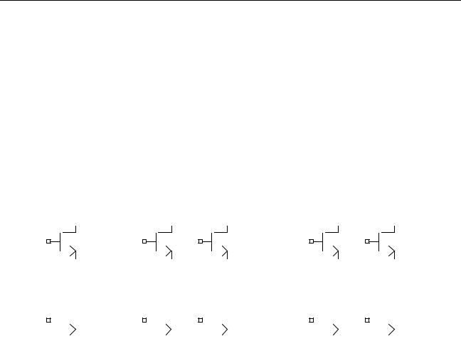
To see the significance of pseudo-parallel nets, consider a symmetric series of N-transistors, A and B, tied in a series pulldown chain to ground, as shown in the following figure.
Both A and B are folded into two legs, with A1, net_PP, and B1 connected in series to ground, and likewise A2 and B2 connected in series to ground, with both pairs in parallel. The nodes between A1 and B1 and between A2 and B2 are electrically equivalent. In reality no current passes through that connection and it need not physically be made.
Original circuit |
Folded circuit with |
|
|
Equivalent Folded circuit with |
|||||||||||||||||||||||||||||||||||
|
|
|
|
|
|
pseudo-parallel connection |
pseudo-parallel net removed |
||||||||||||||||||||||||||||||||
|
|
|
|
|
A |
|
|
|
|
|
|
|
|
A1 |
|
A2 |
|
|
|
|
|
|
|
|
A1 |
|
A2 |
||||||||||||
|
|
|
|
|
|
|
|
|
|
|
|
|
|
|
|
|
|
|
|
|
|
|
|||||||||||||||||
|
|
|
|
|
|
|
|
|
|
|
|
|
|
|
|
|
|
|
|
|
|
|
|||||||||||||||||
|
|
|
|
|
|
|
|
|
|||||||||||||||||||||||||||||||
|
|
|
|
|
|
|
|
|
|
|
|
|
|
|
|
|
|
|
|
|
|
|
|
|
|
|
|
|
|
|
|
|
|
|
|
|
|
|
|
|
|
|
|
|
|
|
|
|
|
|
|
|
|
|
|
|
|
|
|
|
|
|
|
|
|
|
|
|
|
|
|
|
|
|
|
|
|
|
|
|
|
|
|
|
|
|
|
|
|
|
|
|
|
|
|
|
|
|
|
|
|
|
|
|
|
|
|
|
|
|
|
|
|
|
|
|
|
|
|
|
|
|
|
|
|
|
|
|
|
|
|
|
|
|
|
|
|
|
|
|
|
|
|
|
|
|
|
|
|
|
|
|
|
|
|
|
|
|
|
|
|
|
|
|
|
|
|
|
|
|
|
|
|
|
|
|
|
|
|
|
|
|
|
|
|
|
|
|
|
|
|
|
|
|
|
|
|
|
|
|
|
|
|
|
|
|
|
|
|
|
|
|
|
net_PP |
|
|
|
|
|
|
|
|
|
|
|
|
|
|
|
|
|
|
|
||||||
|
|
|
|
|
|
|
|
|
|
|
|
|
|
|
|
|
|
|
|
|
|
|
|
|
|
|
|
|
|
|
|
|
|
|
|
|
|
|
|
|
|
|
|
|
B |
|
|
|
|
|
|
|
|
B1 |
|
|
|
|
|
B2 |
|
|
|
|
|
|
|
|
B1 |
|
|
|
|
|
B2 |
||||
|
|
|
|
|
|
|
|
|
|
|
|
|
|
|
|
|
|
|
|
|
|
|
|
|
|
|
|
|
|
|
|||||||||
|
|
|
|
|
|
|
|
|
|
|
|
|
|
|
|
|
|
|
|
|
|
|
|
|
|
|
|
|
|||||||||||
|
|
|
|
|
|
|
|
|
|
|
|
|
|
|
|
|
|||||||||||||||||||||||
|
|
|
|
|
|
|
|
|
|
|
|
|
|||||||||||||||||||||||||||
|
|
|
|
|
|
|
|
|
|
|
|
|
|
|
|
|
|
|
|
|
|
|
|
|
|
|
|
|
|
|
|
|
|
|
|
|
|
|
|
|
|
|
|
|
|
|
|
|
|
|
|
|
|
|
|
|
|
|
|
|
|
|
|
|
|
|
|
|
|
|
|
|
|
|
|
|
|
|
|
|
|
|
|
|
|
|
|
|
|
|
|
|
|
|
|
|
|
|
|
|
|
|
|
|
|
|
|
|
|
|
|
|
|
|
|
|
|
|
|
|
|
|
|
|
|
|
|
|
|
|
|
|
|
|
|
|
|
|
|
|
|
|
|
|
|
|
|
|
|
|
|
|
|
|
|
|
|
|
|
|
|
|
|
|
|
|
|
|
|
|
|
|
|
|
|
|
|
|
|
|
|
|
|
|
|
|
|
|
|
|
|
|
|
|
|
|
|
|
|
The Assura™ ® verification tool understands pseudo-parallel connections and does not report incomplete nets in such situations.
lxStackPartitionParameters
Sets the device stacking partition parameters. The value is a list of two items. Use the values (-1 -1) to let Virtuoso XL decide how to handle each stack. The default values are (1 8).
The first value controls how far up in the hierarchy Virtuoso XL looks for opportunities to abut devices starting from the leaf node. A value of 1 permits abutment of devices within the same gate only. A value of 2 permits abutment of any devices with the same parent 2 levels from the leaf node. Higher values permit abutment with devices at progressively higher levels of the design hierarchy.
December 2002 |
262 |
Product Version 5.0 |