


 ATmega128
External Memory
Control Register B –
XMCRB
Bit |
7 |
6 |
5 |
4 |
3 |
2 |
1 |
0 |
|
|
XMBK |
– |
– |
– |
– |
XMM2 |
XMM1 |
XMM0 |
XMCRB |
|
|
|
|
|
|
|
|
|
|
Read/Write |
R/W |
R |
R |
R |
R |
R/W |
R/W |
R/W |
|
Initial Value |
0 |
0 |
0 |
0 |
0 |
0 |
0 |
0 |
|
• Bit 7– XMBK: External Memory Bus-keeper Enable
Writing XMBK to one enables the bus keeper on the AD7:0 lines. When the bus keeper is enabled, it will ensure a defined logic level (zero or one) on AD7:0 when they would otherwise be tri-stated. Writing XMBK to zero disables the bus keeper. XMBK is not qualified with SRE, so even if the XMEM interface is disabled, the bus keepers are still activated as long as XMBK is one.
• Bit 6..4 – Res: Reserved Bits
These are reserved bits and will always read as zero. When writing to this address location, write these bits to zero for compatibility with future devices.
• Bit 2..0 – XMM2, XMM1, XMM0: External Memory High Mask
When the External Memory is enabled, all Port C pins are default used for the high address byte. If the full 60 Kbyte address space is not required to access the External Memory, some, or all, Port C pins can be released for normal Port Pin function as described in Table 5. As described in “Using all 64 Kbyte Locations of External Memory” on page 34, it is possible to use the XMMn bits to access all 64 Kbyte locations of the External Memory.
Using all Locations of External Memory Smaller than 64 Kbyte
Table 5. Port C Pins Released as Normal Port Pins when the External Memory is Enabled
XMM2 |
XMM1 |
XMM0 |
# Bits for External Memory Address |
Released Port Pins |
|
|
|
|
|
0 |
0 |
0 |
8 (Full 60 Kbyte space) |
None |
|
|
|
|
|
0 |
0 |
1 |
7 |
PC7 |
|
|
|
|
|
0 |
1 |
0 |
6 |
PC7 - PC6 |
|
|
|
|
|
0 |
1 |
1 |
5 |
PC7 - PC5 |
|
|
|
|
|
1 |
0 |
0 |
4 |
PC7 - PC4 |
|
|
|
|
|
1 |
0 |
1 |
3 |
PC7 - PC3 |
|
|
|
|
|
1 |
1 |
0 |
2 |
PC7 - PC2 |
|
|
|
|
|
1 |
1 |
1 |
No Address high bits |
Full Port C |
|
|
|
|
|
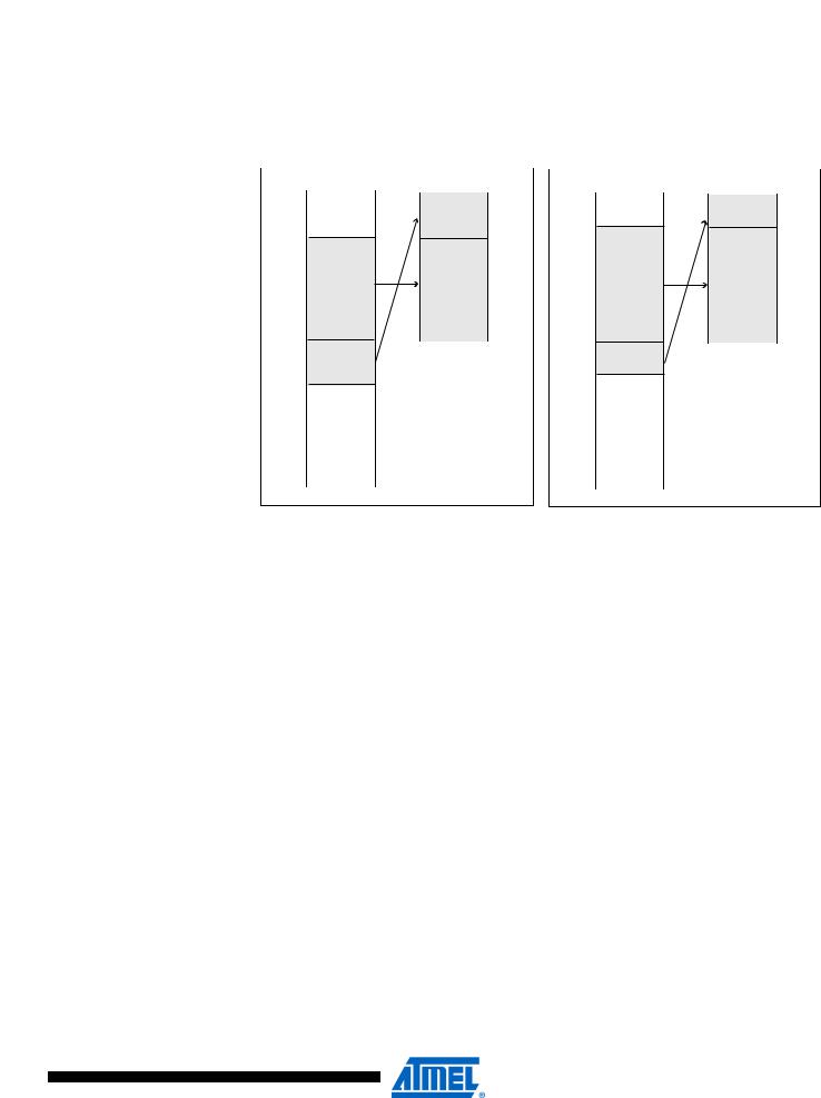
Since the external memory is mapped after the internal memory as shown in Figure 11, the external memory is not addressed when addressing the first 4,352 bytes of data space. It may appear that the first 4,352 bytes of the external memory are inaccessible (external memory addresses 0x0000 to 0x10FF). However, when connecting an external memory smaller than 64 Kbyte, for example 32 Kbyte, these locations are easily accessed simply by addressing from address 0x8000 to 0x90FF. Since the External Memory Address bit A15 is not connected to the external memory, addresses 0x8000 to 0x90FF will appear as addresses 0x0000 to 0x10FF for the external memory. Addressing above address 0x90FF is not recommended, since this will address an external memory location that is already accessed by another (lower) address. To the Application software, the external 32 Kbyte memory will appear as one linear 32 Kbyte address space from 0x1100 to 0x90FF. This is illustrated in Figure 17. Memory configuration B refers to the ATmega103 compatibility mode, configuration A to the non-compatible mode.
When the device is set in ATmega103 compatibility mode, the internal address space is 4,096 bytes. This implies that the first 4,096 bytes of the external memory can be accessed at
32
2467X–AVR–06/11
 ATmega128
addresses 0x8000 to 0x8FFF. To the Application software, the external 32 Kbyte memory will appear as one linear 32 Kbyte address space from 0x1000 to 0x8FFF.
Figure 17. Address Map with 32 Kbyte External Memory
|
|
Memory Configuration A |
|
|
|
Memory Configuration B |
||||||
|
|
|
|
|
|
|
|
|
|
|
|
|
|
|
AVR Memory Map |
|
External 32K SRAM |
|
|
|
|
|
|
||
|
|
|
|
|
|
AVR Memory Map |
|
External 32K SRAM |
||||
0x0000 |
|
|
|
|
0x0000 |
|
0x0000 |
|
|
|
|
0x0000 |
|
Internal Memory |
|
|
|
|
Internal Memory |
|
|
||||
|
|
|
|
|
|
0x0FFF |
|
|
0x0FFF |
|||
|
|
|
|
|
|
|
|
|
|
|||
0x10FF |
|
|
|
0x10FF |
|
0x1000 |
|
|
|
0x1000 |
||
0x1100 |
|
|
0x1100 |
|
|
|
|
|
|
|
||
0x7FFF |
External |
|
|
0x7FFF |
0x7FFF |
External |
|||
|
|
|
|
|
|
0x7FFF |
|||
0x8000 |
Memory |
|
|
|
0x8000 |
Memory |
|||
0x90FF |
|
|
|
|
0x8FFF |
|
|
|
|
0x9100 |
|
|
|
|
0x9000 |
|
|
|
|
|
(Unused) |
|
|
|
|
(Unused) |
|||
0xFFFF |
|
|
|
|
0xFFFF |
|
|
|
|
|
|
|
|
|
|
|
|
||
33
2467X–AVR–06/11
 ATmega128
Using all 64 Kbyte Since the External Memory is mapped after the Internal Memory as shown in Figure 11, only 60 Locations of External Kbyte of External Memory is available by default (address space 0x0000 to 0x10FF is reserved Memory for internal memory). However, it is possible to take advantage of the entire External Memory by masking the higher address bits to zero. This can be done by using the XMMn bits and control by software the most significant bits of the address. By setting Port C to output 0x00, and releasing the most significant bits for normal Port Pin operation, the Memory Interface will address
0x0000 - 0x1FFF. See the following code examples.
Assembly Code Example(1)
;OFFSET is defined to 0x2000 to ensure
;external memory access
;Configure Port C (address high byte) to
;output 0x00 when the pins are released
;for normal Port Pin operation
ldi r16, 0xFF out DDRC, r16 ldi r16, 0x00 out PORTC, r16 ; release PC7:5
ldi r16, (1<<XMM1)|(1<<XMM0) sts XMCRB, r16
;write 0xAA to address 0x0001 of external
;memory
ldi r16, 0xaa
sts 0x0001+OFFSET, r16
;re-enable PC7:5 for external memory ldi r16, (0<<XMM1)|(0<<XMM0)
sts XMCRB, r16
;store 0x55 to address (OFFSET + 1) of
;external memory
ldi r16, 0x55
sts 0x0001+OFFSET, r16
C Code Example(1)
#define OFFSET 0x2000
void XRAM_example(void)
{
unsigned char *p = (unsigned char *) (OFFSET + 1);
DDRC = 0xFF;
PORTC = 0x00;
XMCRB = (1<<XMM1) | (1<<XMM0);
*p = 0xaa;
XMCRB = 0x00;
*p = 0x55;
}
Note: 1. See “About Code Examples” on page 8.
Care must be exercised using this option as most of the memory is masked away.
34
2467X–AVR–06/11