


 ATmega128
I/O Memory
External Memory
Interface
ation is in progress, the write operation will be completed provided that the power supply voltage is sufficient.
The I/O space definition of the ATmega128 is shown in “Register Summary” on page 362.
All Atmel® AVR®ATmega128 I/Os and peripherals are placed in the I/O space. All I/O locations may be accessed by the LD/LDS/LDD and ST/STS/STD instructions, transferring data between the 32 general purpose working registers and the I/O space. I/O registers within the address range $00 - $1F are directly bit-accessible using the SBI and CBI instructions. In these registers, the value of single bits can be checked by using the SBIS and SBIC instructions. Refer to the instruction set section for more details. When using the I/O specific commands IN and OUT, the I/O addresses $00 - $3F must be used. When addressing I/O registers as data space using LD and ST instructions, $20 must be added to these addresses. The ATmega128 is a complex microcontroller with more peripheral units than can be supported within the 64 location reserved in Opcode for the IN and OUT instructions. For the Extended I/O space from $60 - $FF in SRAM, only the ST/STS/STD and LD/LDS/LDD instructions can be used. The Extended I/O space is replaced with SRAM locations when the ATmega128 is in the ATmega103 compatibility mode.
For compatibility with future devices, reserved bits should be written to zero if accessed. Reserved I/O memory addresses should never be written.
Some of the status flags are cleared by writing a logical one to them. Note that the CBI and SBI instructions will operate on all bits in the I/O register, writing a one back into any flag read as set, thus clearing the flag. The CBI and SBI instructions work with registers $00 to $1F only.
The I/O and peripherals control registers are explained in later sections.
With all the features the External Memory Interface provides, it is well suited to operate as an interface to memory devices such as External SRAM and Flash, and peripherals such as LCDdisplay, A/D, and D/A. The main features are:
•Four different wait-state settings (including no wait-state).
•Independent wait-state setting for different extErnal Memory sectors (configurable sector size).
•The number of bits dedicated to address high byte is selectable.
•Bus-keepers on data lines to minimize current consumption (optional).
Overview |
When the eXternal MEMory (XMEM) is enabled, address space outside the internal SRAM |
|
becomes available using the dedicated External Memory pins (see Figure 1 on page 2, Table 27 |
|
on page 72, Table 33 on page 76, and Table 45 on page 84). The memory configuration is |
|
shown in Figure 11. |
25
2467X–AVR–06/11
 ATmega128
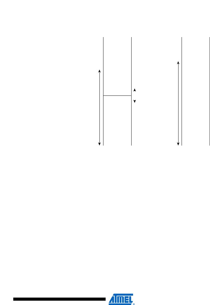
Figure 11. External Memory with Sector Select
Memory Configuration A |
Memory Configuration B |
||||||
|
|
0x0000 |
|
|
0x0000 |
||
|
Internal memory |
Internal memory |
|||||
|
|
|
|
|
|||
|
|
|
|
|
|
0x0FFF |
|
|
|
0x10FF |
|
|
0x1000 |
||
|
|
|
|
|
|||
|
|
0x1100 |
|
|
|
||
|
Lower sector |
|
|
|
|||
|
SRW01 |
|
|
|
|||
|
SRW00 |
|
|
|
|||
|
|
|
SRL[2..0] |
|
SRW10 |
||
|
|
|
|
||||
|
|
|
|
|
|
||
External Memory |
|
|
|
External Memory |
|||
Upper sector |
|||||||
(0-60K x 8) |
(0-60K x 8) |
||||||
|
|
|
|||||
|
SRW11 |
|
|
|
|||
|
SRW10 |
|
|
|
|||
|
|
|
|
|
|
|
0xFFFF |
|
0xFFFF |
|
Note: ATmega128 in non ATmega103 compatibility mode: Memory Configuration A is available (Memory |
||||||||
|
|
|
Configuration B N/A) |
|
|||||
|
|
|
ATmega128 in ATmega103 compatibility mode: Memory Configuration B is available (Memory |
||||||
|
|
|
Configuration A N/A) |
|
|||||
ATmega103 |
Both External Memory Control Registers (XMCRA and XMCRB) are placed in Extended I/O |
||||||||
Compatibility |
space. In ATmega103 compatibility mode, these registers are not available, and the features |
||||||||
|
selected by these registers are not available. The device is still ATmega103 compatible, as |
||||||||
|
these features did not exist in ATmega103. The limitations in ATmega103 compatibility mode |
||||||||
|
are: |
|
|||||||
|
• Only two wait-states settings are available (SRW1n = 0b00 and SRW1n = 0b01). |
||||||||
|
• The number of bits that are assigned to address high byte are fixed. |
|
|||||||
|
• The External Memory section can not be divided into sectors with different wait-state |
||||||||
|
|
settings. |
|
||||||
|
• Bus-keeper is not available. |
|
|||||||
|
• |
|
|
|
and ALE pins are output only (Port G in ATmega128). |
|
|||
|
RD, |
WR |
|
||||||
Using the External |
The interface consists of: |
|
|||||||
Memory Interface |
• AD7:0: Multiplexed low-order address bus and data bus. |
|||
|
||||
|
• A15:8: High-order address bus (configurable number of bits). |
|||
|
• ALE: Address latch enable. |
|||
|
• |
|
|
Read strobe. |
|
RD: |
|||
|
• |
|
Write strobe. |
|
|
WR: |
|||
26
2467X–AVR–06/11
 ATmega128
The control bits for the External Memory Interface are located in three registers, the MCU Control Register – MCUCR, the External Memory Control Register A – XMCRA, and the External Memory Control Register B – XMCRB.
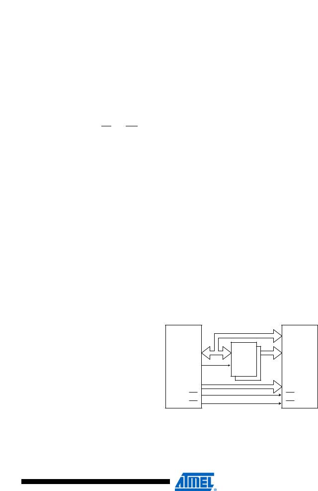
When the XMEM interface is enabled, the XMEM interface will override the setting in the data direction registers that corresponds to the ports dedicated to the XMEM interface. For details about the port override, see the alternate functions in section “I/O Ports” on page 65. The XMEM interface will auto-detect whether an access is internal or external. If the access is external, the XMEM interface will output address, data, and the control signals on the ports according to Figure 13 (this figure shows the wave forms without wait-states). When ALE goes from high-to-low, there is a valid address on AD7:0. ALE is low during a data transfer. When the XMEM interface is enabled, also an internal access will cause activity on address, data and ALE ports, but the RD and WR strobes will not toggle during internal access. When the External Memory Interface is disabled, the normal pin and data direction settings are used. Note that when the XMEM interface is disabled, the address space above the internal SRAM boundary is not mapped into the internal SRAM. Figure 12 illustrates how to connect an external SRAM to the AVR using an octal latch (typically “74 x 573” or equivalent) which is transparent when G is high.
Address Latch |
Due to the high-speed operation of the XRAM interface, the address latch must be selected with |
Requirements |
care for system frequencies above 8MHz @ 4V and 4MHz @ 2.7V. When operating at condi- |
|
tions above these frequencies, the typical old style 74HC series latch becomes inadequate. The |
|
External Memory Interface is designed in compliance to the 74AHC series latch. However, most |
|
latches can be used as long they comply with the main timing parameters. The main parameters |
|
for the address latch are: |
•D to Q propagation delay (tPD).
•Data setup time before G low (tSU).
•Data (address) hold time after G low (TH).
The External Memory Interface is designed to guaranty minimum address hold time after G is
asserted low of th = 5 ns. Refer to tLAXX_LD/tLLAXX_ST in “External Data Memory Timing” Tables 137 through Tables 144 on pages 328 - 330. The D-to-Q propagation delay (tPD) must be taken
into consideration when calculating the access time requirement of the external component. The
data setup time before G low (tSU) must not exceed address valid to ALE low (tAVLLC) minus PCB wiring delay (dependent on the capacitive load).
Figure 12. External SRAM Connected to the AVR
|
|
|
D[7:0] |
AD7:0 |
D |
Q |
A[7:0] |
ALE |
G |
|
SRAM |
AVR |
|
|
|
|
|
|
|
A15:8 |
|
|
A[15:8] |
RD |
|
|
RD |
WR |
|
|
WR |
27
2467X–AVR–06/11
 ATmega128
Pull-up and Bus- |
The pull-ups on the AD7:0 ports may be activated if the corresponding Port register is written to |
keeper |
one. To reduce power consumption in sleep mode, it is recommended to disable the pull-ups by |
|
writing the Port register to zero before entering sleep. |
|
The XMEM interface also provides a bus-keeper on the AD7:0 lines. The bus-keeper can be dis- |
|
abled and enabled in software as described in “External Memory Control Register B – XMCRB” |
|
on page 32. When enabled, the bus-keeper will ensure a defined logic level (zero or one) on the |
|
AD7:0 bus when these lines would otherwise be tri-stated by the XMEM interface. |
Timing |
External Memory devices have different timing requirements. To meet these requirements, the |
|
ATmega128 XMEM interface provides four different wait-states as shown in Table 4. It is impor- |
|
tant to consider the timing specification of the External Memory device before selecting the wait- |
|
state. The most important parameters are the access time for the external memory compared to |
|
the set-up requirement of the ATmega128. The access time for the External Memory is defined |
|
to be the time from receiving the chip select/address until the data of this address actually is |
|
driven on the bus. The access time cannot exceed the time from the ALE pulse must be |
|
asserted low until data is stable during a read sequence (See tLLRL+ tRLRH - tDVRH in Tables 137 |
|
through Tables 144 on pages 328 - 330). The different wait-states are set up in software. As an |
|
additional feature, it is possible to divide the external memory space in two sectors with individ- |
|
ual wait-state settings. This makes it possible to connect two different memory devices with |
|
different timing requirements to the same XMEM interface. For XMEM interface timing details, |
|
please refer to Table 137 to Table 144 and Figure 157 to Figure 160 in the “External Data Mem- |
|
ory Timing” on page 328. |
|
Note that the XMEM interface is asynchronous and that the waveforms in the following figures |
|
are related to the internal system clock. The skew between the internal and external clock |
|
(XTAL1) is not guarantied (varies between devices temperature, and supply voltage). Conse- |
|
quently, the XMEM interface is not suited for synchronous operation. |
|
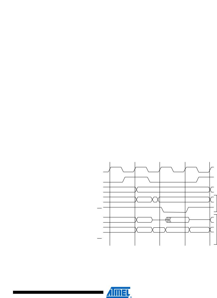
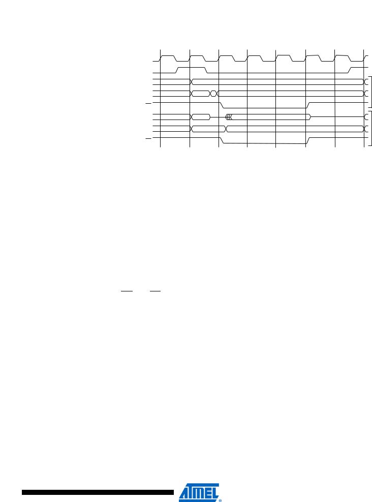
Figure 13. External Data Memory Cycles without Wait-state (SRWn1=0 and SRWn0=0) |
|
T1 |
T2 |
|
T3 |
T4 |
System Clock (CLKCPU) |
|
|
|
|
|
ALE |
|
|
|
|
|
A15:8 |
Prev. addr. |
|
|
Address |
|
DA7:0 |
Prev. data |
Address |
XX |
Data |
|
WR |
|
|
|
|
|
DA7:0 (XMBK = 0) |
Prev. data |
Address |
|
Data |
|
DA7:0 (XMBK = 1) |
Prev. data |
Address |
XXXXX |
Data |
XXXXXXXX |
Write
Read
RD 
Note: 1. SRWn1 = SRW11 (upper sector) or SRW01 (lower sector), SRWn0 = SRW10 (upper sector) or SRW00 (lower sector). The ALE pulse in period T4 is only present if the next instruction accesses the RAM (internal or external).
28
2467X–AVR–06/11
 ATmega128
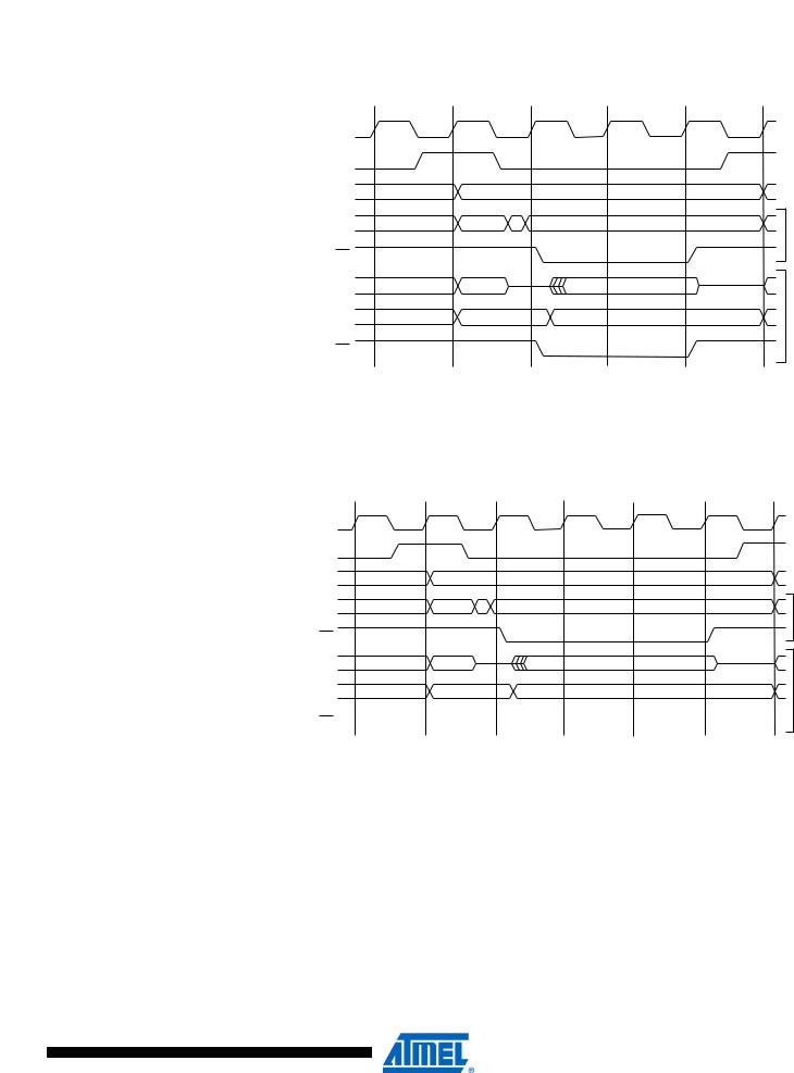
Figure 14. External Data Memory Cycles with SRWn1 = 0 and SRWn0 = 1(1)
|
T1 |
T2 |
T3 |
T4 |
T5 |
System Clock (CLKCPU) |
|
|
|
|
|
ALE |
|
|
|
|
|
A15:8 |
Prev. addr. |
|
Address |
|
|
DA7:0 |
Prev. data |
Address XX |
Data |
|
|
WR |
|
|
|
|
|
DA7:0 (XMBK = 0) |
Prev. data |
Address |
Data |
|
|
DA7:0 (XMBK = 1) |
Prev. data |
Address |
Data |
|
|
RD |
|
|
|
|
|
Read Write
Note: 1. SRWn1 = SRW11 (upper sector) or SRW01 (lower sector), SRWn0 = SRW10 (upper sector) or SRW00 (lower sector).
The ALE pulse in period T5 is only present if the next instruction accesses the RAM (internal or external).
Figure 15. External Data Memory Cycles with SRWn1 = 1 and SRWn0 = 0(1)
|
T1 |
T2 |
T3 |
T4 |
T5 |
T6 |
System Clock (CLKCPU) |
|
|
|
|
|
|
ALE |
|
|
|
|
|
|
A15:8 |
Prev. addr. |
|
Address |
|
|
|
DA7:0 |
Prev. data |
Address XX |
Data |
|
|
|
WR |
|
|
|
|
|
|
DA7:0 (XMBK = 0) |
Prev. data |
Address |
Data |
|
|
|
DA7:0 (XMBK = 1) |
Prev. data |
Address |
Data |
|
|
|
Read Write
RD 
Note: 1. SRWn1 = SRW11 (upper sector) or SRW01 (lower sector), SRWn0 = SRW10 (upper sector) or SRW00 (lower sector).
The ALE pulse in period T6 is only present if the next instruction accesses the RAM (internal or external).
29
2467X–AVR–06/11
 ATmega128
Figure 16. External Data Memory Cycles with SRWn1 = 1 and SRWn0 = 1(1)
|
T1 |
T2 |
T3 |
T4 |
T5 |
T6 |
T7 |
System Clock (CLKCPU) |
|
|
|
|
|
|
|
ALE |
|
|
|
|
|
|
|
A15:8 |
Prev. addr. |
|
Address |
|
|
|
|
DA7:0 |
Prev. data |
Address XX |
Data |
|
|
|
|
WR |
|
|
|
|
|
|
|
DA7:0 (XMBK = 0) |
Prev. data |
Address |
Data |
|
|
|
|
DA7:0 (XMBK = 1) |
Prev. data |
Address |
Data |
|
|
|
|
RD |
|
|
|
|
|
|
|
Write
Read
Note: 1. SRWn1 = SRW11 (upper sector) or SRW01 (lower sector), SRWn0 = SRW10 (upper sector) or SRW00 (lower sector).
The ALE pulse in period T7 is only present if the next instruction accesses the RAM (internal or external).
XMEM Register
Description
MCU Control Register
– MCUCR
Bit |
7 |
6 |
5 |
4 |
3 |
2 |
1 |
0 |
|
|
SRE |
SRW10 |
SE |
SM1 |
SM0 |
SM2 |
IVSEL |
IVCE |
MCUCR |
Read/Write |
R/W |
R/W |
R/W |
R/W |
R/W |
R/W |
R/W |
R/W |
|
Initial Value |
0 |
0 |
0 |
0 |
0 |
0 |
0 |
0 |
|
• Bit 7 – SRE: External SRAM/XMEM Enable
External Memory
Control Register A –
XMCRA
Writing SRE to one enables the External Memory Interface.The pin functions AD7:0, A15:8, ALE, WR, and RD are activated as the alternate pin functions. The SRE bit overrides any pin direction settings in the respective data direction registers. Writing SRE to zero, disables the External Memory Interface and the normal pin and data direction settings are used.
• Bit 6 – SRW10: Wait-state Select Bit
For a detailed description in non-ATmega103 compatibility mode, see common description for the SRWn bits below (XMCRA description). In ATmega103 compatibility mode, writing SRW10 to one enables the wait-state and one extra cycle is added during read/write strobe as shown in Figure 14.
Bit |
7 |
6 |
5 |
4 |
3 |
2 |
1 |
0 |
|
|
– |
SRL2 |
SRL1 |
SRL0 |
SRW01 |
SRW00 |
SRW11 |
– |
XMCRA |
|
|
|
|
|
|
|
|
|
|
Read/Write |
R |
R/W |
R/W |
R/W |
R/W |
R/W |
R/W |
R |
|
Initial Value |
0 |
0 |
0 |
0 |
0 |
0 |
0 |
0 |
|
• Bit 7 – Res: Reserved Bit
This is a reserved bit and will always read as zero. When writing to this address location, write this bit to zero for compatibility with future devices.
30
2467X–AVR–06/11
 ATmega128
• Bit 6..4 – SRL2, SRL1, SRL0: Wait-state Sector Limit
It is possible to configure different wait-states for different External Memory addresses. The external memory address space can be divided in two sectors that have separate wait-state bits. The SRL2, SRL1, and SRL0 bits select the split of the sectors, see Table 3 and Figure 11. By default, the SRL2, SRL1, and SRL0 bits are set to zero and the entire external memory address space is treated as one sector. When the entire SRAM address space is configured as one sector, the wait-states are configured by the SRW11 and SRW10 bits.
Table 3. Sector limits with different settings of SRL2..0
SRL2 |
SRL1 |
SRL0 |
Sector Limits |
|
|
|
|
0 |
0 |
0 |
Lower sector = N/A |
|
|
|
Upper sector = 0x1100 - 0xFFFF |
|
|
|
|
0 |
0 |
1 |
Lower sector = 0x1100 - 0x1FFF |
|
|
|
Upper sector = 0x2000 - 0xFFFF |
|
|
|
|
0 |
1 |
0 |
Lower sector = 0x1100 - 0x3FFF |
|
|
|
Upper sector = 0x4000 - 0xFFFF |
|
|
|
|
0 |
1 |
1 |
Lower sector = 0x1100 - 0x5FFF |
|
|
|
Upper sector = 0x6000 - 0xFFFF |
|
|
|
|
1 |
0 |
0 |
Lower sector = 0x1100 - 0x7FFF |
|
|
|
Upper sector = 0x8000 - 0xFFFF |
|
|
|
|
1 |
0 |
1 |
Lower sector = 0x1100 - 0x9FFF |
|
|
|
Upper sector = 0xA000 - 0xFFFF |
|
|
|
|
1 |
1 |
0 |
Lower sector = 0x1100 - 0xBFFF |
|
|
|
Upper sector = 0xC000 - 0xFFFF |
|
|
|
|
1 |
1 |
1 |
Lower sector = 0x1100 - 0xDFFF |
|
|
|
Upper sector = 0xE000 - 0xFFFF |
|
|
|
|
• Bit 1 and Bit 6 MCUCR – SRW11, SRW10: Wait-state Select Bits for Upper Sector
The SRW11 and SRW10 bits control the number of wait-states for the upper sector of the external memory address space, see Table 4.
• Bit 3..2 – SRW01, SRW00: Wait-state Select Bits for Lower Sector
The SRW01 and SRW00 bits control the number of wait-states for the lower sector of the external memory address space, see Table 4.
Table 4. Wait States(1)
SRWn1 |
SRWn0 |
Wait States |
|
|
|
|
|
0 |
0 |
No wait-states |
|
|
|
|
|
0 |
1 |
Wait one cycle during read/write strobe |
|
|
|
|
|
1 |
0 |
Wait two cycles during read/write strobe |
|
|
|
|
|
1 |
1 |
Wait two cycles during read/write and wait one cycle before driving out |
|
|
|
new address |
|
|
|
|
|
Note: 1. |
n = 0 or 1 (lower/upper sector). |
||
|
For further details of the timing and wait-states of the External Memory Interface, see Figures |
||
|
13 through Figures 16 for how the setting of the SRW bits affects the timing. |
||
• Bit 0 – Res: Reserved Bit
This is a reserved bit and will always read as zero. When writing to this address location, write this bit to zero for compatibility with future devices.
31
2467X–AVR–06/11