

 ATmega128
are generated on the output compare outputs OCnx. For more details about advanced counting sequences and waveform generation, see “Modes of Operation” on page 123.
The Timer/Counter Overflow (TOVn) flag is set according to the mode of operation selected by the WGMn3:0 bits. TOVn can be used for generating a CPU interrupt.
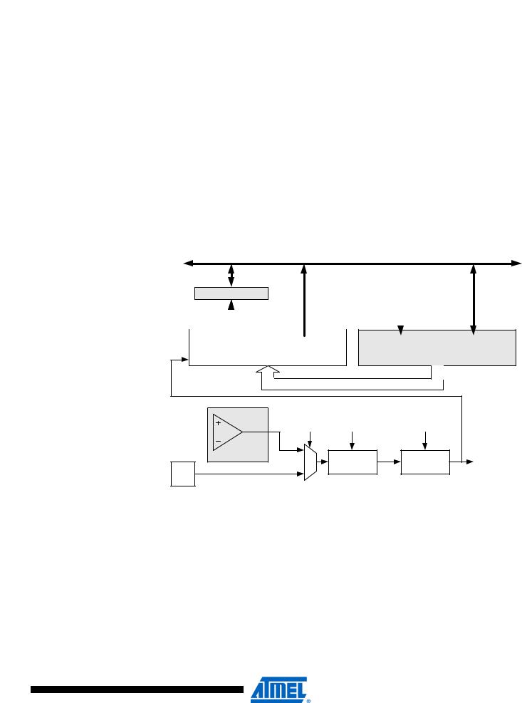
Input Capture Unit The Timer/Counter incorporates an Input Capture unit that can capture external events and give them a time-stamp indicating time of occurrence. The external signal indicating an event, or multiple events, can be applied via the ICPn pin or alternatively, for the Timer/Counter1 only, via the Analog Comparator unit. The time-stamps can then be used to calculate frequency, duty-cycle, and other features of the signal applied. Alternatively the time-stamps can be used for creating a log of the events.
The Input Capture unit is illustrated by the block diagram shown in Figure 48. The elements of the block diagram that are not directly a part of the Input Capture unit are gray shaded. The small “n” in register and bit names indicates the Timer/Counter number.
Figure 48. Input Capture Unit Block Diagram
DATA BUS (8-bit)
TEMP (8-bit)
|
|
|
|
|
|
|
|
|
|
|
|
|
|
|
|
|
|
|
|
|
|
|
|
|
|
|
|
|
|
|
|
|
|
|
|
|
ICRnH (8-bit) |
ICRnL (8-bit) |
|
|
TCNTnH (8-bit) |
TCNTnL (8-bit) |
||
|
|
|
|
|
|
|
|
|
WRITE |
ICRn (16-bit Register) |
|
TCNTn (16-bit Counter) |
|
|
|
ACO* |
ACIC* |
ICNC |
ICES |
|
|
Comparator |
|
Noise |
Edge |
ICFn (Int.Req.) |
|
|
|
|||
|
|
|
Canceler |
Detector |
|
|
|
|
|
||
ICPn |
|
|
|
|
|
Note: The Analog Comparator Output (ACO) can only trigger the Timer/Counter1 ICP – not Timer/Counter3.
When a change of the logic level (an event) occurs on the Input Capture Pin (ICPn), alternatively on the analog Comparator output (ACO), and this change confirms to the setting of the edge detector, a capture will be triggered. When a capture is triggered, the 16-bit value of the counter (TCNTn) is written to the Input Capture Register (ICRn). The Input Capture Flag (ICFn) is set at the same system clock as the TCNTn value is copied into ICRn Register. If enabled (TICIEn = 1), the Input Capture flag generates an Input Capture interrupt. The ICFn flag is automatically cleared when the interrupt is executed. Alternatively the ICFn flag can be cleared by software by writing a logical one to its I/O bit location.
Reading the 16-bit value in the Input Capture Register (ICRn) is done by first reading the low byte (ICRnL) and then the high byte (ICRnH). When the low byte is read the high byte is copied
118
2467X–AVR–06/11

 ATmega128
|
into the high byte Temporary Register (TEMP). When the CPU reads the ICRnH I/O location it |
|
will access the TEMP Register. |
|
The ICRn Register can only be written when using a Waveform Generation mode that utilizes |
|
the ICRn Register for defining the counter’s TOP value. In these cases the Waveform Genera- |
|
tion mode (WGMn3:0) bits must be set before the TOP value can be written to the ICRn |
|
Register. When writing the ICRn Register the high byte must be written to the ICRnH I/O location |
|
before the low byte is written to ICRnL. |
|
For more information on how to access the 16-bit registers refer to “Accessing 16-bit Registers” |
|
on page 114. |
Input Capture Pin |
The main trigger source for the Input Capture unit is the Input Capture Pin (ICPn). |
Source |
Timer/Counter1 can alternatively use the analog comparator output as trigger source for the |
|
Input Capture unit. The Analog Comparator is selected as trigger source by setting the analog |
|
Comparator Input Capture (ACIC) bit in the Analog Comparator Control and Status Register |
|
(ACSR). Be aware that changing trigger source can trigger a capture. The Input Capture flag |
|
must therefore be cleared after the change. |
|
Both the Input Capture Pin (ICPn) and the Analog Comparator output (ACO) inputs are sampled |
|
using the same technique as for the Tn pin (Figure 59 on page 143). The edge detector is also |
|
identical. However, when the noise canceler is enabled, additional logic is inserted before the |
|
edge detector, which increases the delay by four system clock cycles. Note that the input of the |
|
noise canceler and edge detector is always enabled unless the Timer/Counter is set in a Wave- |
|
form Generation mode that uses ICRn to define TOP. |
|
An Input Capture can be triggered by software by controlling the port of the ICPn pin. |
Noise Canceler |
The noise canceler improves noise immunity by using a simple digital filtering scheme. The |
|
noise canceler input is monitored over four samples, and all four must be equal for changing the |
|
output that in turn is used by the edge detector. |
|
The noise canceler is enabled by setting the Input Capture Noise Canceler (ICNCn) bit in |
|
Timer/Counter Control Register B (TCCRnB). When enabled the noise canceler introduces addi- |
|
tional four system clock cycles of delay from a change applied to the input, to the update of the |
|
ICRn Register. The noise canceler uses the system clock and is therefore not affected by the |
|
prescaler. |
Using the Input |
The main challenge when using the Input Capture unit is to assign enough processor capacity |
Capture Unit |
for handling the incoming events. The time between two events is critical. If the processor has |
|
not read the captured value in the ICRn Register before the next event occurs, the ICRn will be |
|
overwritten with a new value. In this case the result of the capture will be incorrect. |
|
When using the Input Capture interrupt, the ICRn Register should be read as early in the inter- |
|
rupt handler routine as possible. Even though the Input Capture interrupt has relatively high |
|
priority, the maximum interrupt response time is dependent on the maximum number of clock |
|
cycles it takes to handle any of the other interrupt requests. |
|
Using the Input Capture unit in any mode of operation when the TOP value (resolution) is |
|
actively changed during operation, is not recommended. |
|
Measurement of an external signal’s duty cycle requires that the trigger edge is changed after |
|
each capture. Changing the edge sensing must be done as early as possible after the ICRn |
|
Register has been read. After a change of the edge, the Input Capture flag (ICFn) must be |
|
cleared by software (writing a logical one to the I/O bit location). For measuring frequency only, |
|
the clearing of the ICFn flag is not required (if an interrupt handler is used). |
119
2467X–AVR–06/11
 ATmega128
Output Compare
Units
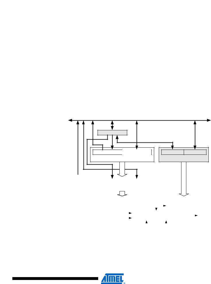
The 16-bit comparator continuously compares TCNTn with the Output Compare Register (OCRnx). If TCNT equals OCRnx the comparator signals a match. A match will set the Output Compare Flag (OCFnx) at the next timer clock cycle. If enabled (OCIEnx = 1), the output compare flag generates an output compare interrupt. The OCFnx flag is automatically cleared when the interrupt is executed. Alternatively the OCFnx flag can be cleared by software by writing a logical one to its I/O bit location. The Waveform Generator uses the match signal to generate an output according to operating mode set by the Waveform Generation mode (WGMn3:0) bits and Compare Output mode (COMnx1:0) bits. The TOP and BOTTOM signals are used by the waveform generator for handling the special cases of the extreme values in some modes of operation (See “Modes of Operation” on page 123.)
A special feature of output compare unit A allows it to define the Timer/Counter TOP value (i.e., counter resolution). In addition to the counter resolution, the TOP value defines the period time for waveforms generated by the waveform generator.
Figure 49 shows a block diagram of the output compare unit. The small “n” in the register and bit names indicates the device number (n = n for Timer/Counter n), and the “x” indicates output compare unit (A/B/C). The elements of the block diagram that are not directly a part of the output compare unit are gray shaded.
Figure 49. Output Compare Unit, Block Diagram |
|
|
|
|
DATABUS (8-bit) |
|
|
TEMP (8-bit) |
|
|
|
OCRnxH Buf. (8-bit) |
OCRnxL Buf. (8-bit) |
TCNTnH (8-bit) |
TCNTnL (8-bit) |
OCRnx Buffer (16-bit Register) |
TCNTn (16-bit Counter) |
||
|
|
|
|
|
|
|
|
|
|
|
|
|
|
|
|
|
|
|
|
|
|
|
|
|
|
|
|
|
|
|
|
|
|
|
|
|
|
|
|
|
OCRnxH (8-bit) |
|
OCRnxL (8-bit) |
|
|
|
|
|
|
|
|
|
||||
|
|
|
|
|
|
|
|
|
|
|
|
|
|
|
|
|||
|
|
|
|
OCRnx (16-bit Register) |
|
|
|
|
|
|
|
|
||||||
|
|
|
|
|
|
|
|
|
|
|
|
|
|
|
|
|
|
|
|
|
|
|
|
|
|
|
|
|
|
|
|
|
|
|
|
|
|
|
|
|
|
|
|
|
|
=(16-bit Comparator ) |
|
|
|
|||||||
|
|
|
|
|
|
|
|
|
|
|
|
|
|
OCFnx (Int.Req.) |
|
|||
|
|
|
|
|
|
|
|
|
|
|
|
|
|
|||||
|
|
|
|
|
|
|
|
|
|
|
|
|
|
|
|
|
|
|
|
|
|
|
TOP |
|
|
|
Waveform Generator |
|
|
|
OCnx |
||||||
|
|
|
|
|
|
|
||||||||||||
|
|
|
BOTTOM |
|
|
|
|
|
||||||||||
|
|
|
|
|
|
|
|
|||||||||||
|
|
|
|
|
|
|
|
|
|
|
|
|
|
|
|
|
||
|
|
|
|
|
|
|
|
|
|
|
|
|
|
|
|
|
||
|
|
|
|
|
|
|
|
|
|
|
|
|
|
|
|
|
|
|
|
|
|
|
|
|
|
|
|
|
|
|
|
|
|
|
|||
|
|
|
|
|
|
|
|
|
|
|
|
|
|
|
|
|
||
|
|
|
|
|
|
|
|
WGMn3:0 |
COMnx1:0 |
|
||||||||
The OCRnx Register is double buffered when using any of the twelve Pulse Width Modulation (PWM) modes. For the normal and Clear Timer on Compare (CTC) modes of operation, the double buffering is disabled. The double buffering synchronizes the update of the OCRnx Compare Register to either TOP or BOTTOM of the counting sequence. The synchronization prevents the occurrence of odd-length, non-symmetrical PWM pulses, thereby making the output glitch-free.
120
2467X–AVR–06/11
 ATmega128
|
The OCRnx Register access may seem complex, but this is not case. When the double buffering |
|
is enabled, the CPU has access to the OCRnx buffer register, and if double buffering is disabled |
|
the CPU will access the OCRnx directly. The content of the OCR1x (buffer or compare) register |
|
is only changed by a write operation (the Timer/Counter does not update this register automati- |
|
cally as the TCNTnand ICRn Register). Therefore OCRnx is not read via the high byte |
|
Temporary Register (TEMP). However, it is a good practice to read the low byte first as when |
|
accessing other 16-bit registers. Writing the OCRnx registers must be done via the TEMP Regis- |
|
ter since the compare of all 16 bits is done continuously. The high byte (OCRnxH) has to be |
|
written first. When the high byte I/O location is written by the CPU, the TEMP Register will be |
|
updated by the value written. Then when the low byte (OCRnxL) is written to the lower 8 bits, the |
|
high byte will be copied into the upper 8 bits of either the OCRnx buffer or OCRnx Compare |
|
Register in the same system clock cycle. |
|
For more information of how to access the 16-bit registers refer to “Accessing 16-bit Registers” |
|
on page 114. |
Force Output |
In non-PWM Waveform Generation modes, the match output of the comparator can be forced by |
Compare |
writing a one to the Force Output Compare (FOCnx) bit. Forcing compare match will not set the |
|
OCFnx flag or reload/clear the timer, but the OCnx pin will be updated as if a real compare |
|
match had occurred (the COMnx1:0 bits settings define whether the OCnx pin is set, cleared or |
|
toggled). |
Compare Match |
All CPU writes to the TCNTn Register will block any compare match that occurs in the next timer |
Blocking by TCNTn |
clock cycle, even when the timer is stopped. This feature allows OCRnx to be initialized to the |
Write |
same value as TCNTn without triggering an interrupt when the Timer/Counter clock is enabled. |
Using the Output |
Since writing TCNTn in any mode of operation will block all compare matches for one timer clock |
Compare Unit |
cycle, there are risks involved when changing TCNTn when using any of the output compare |
|
channels, independent of whether the Timer/Counter is running or not. If the value written to |
|
TCNTn equals the OCRnx value, the compare match will be missed, resulting in incorrect wave- |
|
form generation. Do not write the TCNTn equal to TOP in PWM modes with variable TOP |
|
values. The compare match for the TOP will be ignored and the counter will continue to 0xFFFF. |
|
Similarly, do not write the TCNTn value equal to BOTTOM when the counter is downcounting. |
|
The setup of the OCnx should be performed before setting the Data Direction Register for the |
|
port pin to output. The easiest way of setting the OCnx value is to use the force output compare |
|
(FOCnx) strobe bits in normal mode. The OCnx Register keeps its value even when changing |
|
between waveform generation modes. |
|
Be aware that the COMnx1:0 bits are not double buffered together with the compare value. |
|
Changing the COMnx1:0 bits will take effect immediately. |
121
2467X–AVR–06/11

 ATmega128
Compare Match
Output Unit
The Compare Output mode (COMnx1:0) bits have two functions. The waveform generator uses the COMnx1:0 bits for defining the output compare (OCnx) state at the next compare match. Secondly the COMnx1:0 bits control the OCnx pin output source. Figure 50 shows a simplified schematic of the logic affected by the COMnx1:0 bit setting. The I/O registers, I/O bits, and I/O pins in the figure are shown in bold. Only the parts of the general I/O port control registers (DDR and PORT) that are affected by the COMnx1:0 bits are shown. When referring to the OCnx state, the reference is for the internal OCnx Register, not the OCnx pin. If a system Reset occur, the OCnx Register is reset to “0”.
Figure 50. Compare Match Output Unit, Schematic
COMnx1 |
|
|
|
|
|
|
|
|
|
|
|
|
|
|
|
|
|
|
|
|
|
|
|
|
|
|
|
|
|
|
|
|
|
|
|
|
|
|
|
|
|
|
|
|
|
||
|
|
|
|
|
|
|
|
|
|
|
|
|
|
|
|
|
|
|
|
|
|
||
|
|
|
|
|
|
|
|
|
|
|
|
|
|
|
|
|
|
|
|
|
|
||
|
|
|
|
|
|
|
|
|
|
|
|
|
|
|
|
|
|
|
|
|
|
||
|
Waveform |
|
|
|
|
|
|
|
|
|
|
|
|
|
|
||||||||
|
|
|
|
|
|
|
|
|
|
|
|
|
|
|
|
|
|
|
|||||
COMnx0 |
|
D |
Q |
|
|
|
|
|
|
|
|
|
|||||||||||
|
|
|
|
|
Generator |
|
|
|
|
|
|
|
|
|
|
|
|
||||||
FOCnx |
|
|
|
|
|
|
|
|
|
|
|
|
|
||||||||||
|
|
|
|
|
|
|
|
|
|
|
|
|
|
|
|||||||||
|
|
|
|
|
|
|
|
|
|
|
|
|
|
|
|
|
|
|
|
|
|
|
|
|
|
|
|
|
|
|
|
|
|
|
|
|
|
|
|
|
1 |
|
|
|
|
|
|
|
|
|
|
|
|
|
|
|
|
|
|
|
|
|
|
|
|
|
|
|
|
|
OCnx |
|
|
|
|
|
|
|
|
|
|
|
|
|
OCnx |
|
|
0 |
|
|
|
|
Pin |
||
|
|
|
|
|
|
|
|
|
|
|
|
|
|
|
|
|
|
|
|||||
|
|
|
|
|
|
|
|
|
|
|
|
|
|
|
|
|
|
|
|
|
|
|
|
|
|
|
|
|
|
|
|
BUS |
|
|
|
|
D |
Q |
|
|
|
|
|
|
|
|
|
|
|
|
|
|
|
|
|
|
|
|
|
|
|
|
|
|
|
|
|
|
|||
|
|
|
|
|
|
|
|
|
|
|
|
|
|
|
|
|
|
|
|
|
|||
|
|
|
|
|
|
|
|
|
|
|
|
|
|
|
|
|
|
|
|
|
|
||
|
|
|
|
PORT |
|
|
|
|
|
|
|
|
|
||||||||||
|
|
|
|
|
|
|
|
DATA |
|
|
|
|
|
|
|
|
|
|
|
|
|
|
|
|
|
|
|
D |
Q |
|
|
|
|
|
|
|
|
|
|||||||||
|
|
|
|
|
|
|
|
|
|
|
|
|
|
|
|
|
|
|
|
|
|
||
|
|
|
|
|
|
|
|
|
|
|
|
|
|
|
|
|
|
|
|
|
|
|
|
|
|
|
|
|
|
|
|
|
|
|
|
|
|
|
|
|
|
|
|
|
|
|
|
|
clkI/O |
|
|
|
|
|
|
|
|
|
DDR |
|
|
|
|
|
|
|
|
|
|||
|
|
|
|
|
|
|
|
|
|
|
|
|
|
|
|
|
|
|
|
|
|||
The general I/O port function is overridden by the output compare (OCnx) from the Waveform Generator if either of the COMnx1:0 bits are set. However, the OCnx pin direction (input or output) is still controlled by the Data Direction Register (DDR) for the port pin. The data direction register bit for the OCnx pin (DDR_OCnx) must be set as output before the OCnx value is visible on the pin. The port override function is generally independent of the waveform generation mode, but there are some exceptions. Refer to Table 58, Table 59 and Table 60 for details.
The design of the output compare pin logic allows initialization of the OCnx state before the output is enabled. Note that some COMnx1:0 bit settings are reserved for certain modes of operation. See “16-bit Timer/Counter Register Description” on page 132.
The COMnx1:0 bits have no effect on the Input Capture unit.
Compare Output Mode The waveform generator uses the COMnx1:0 bits differently in normal, CTC, and PWM modes.
and Waveform |
For all modes, setting the COMnx1:0 = 0 tells the waveform generator that no action on the |
Generation |
OCnx Register is to be performed on the next compare match. For compare output actions in the |
|
non-PWM modes refer to Table 58 on page 132. For fast PWM mode refer to Table 59 on page |
|
133, and for phase correct and phase and frequency correct PWM refer to Table 60 on page |
|
133. |
|
A change of the COMnx1:0 bits state will have effect at the first compare match after the bits are |
|
written. For non-PWM modes, the action can be forced to have immediate effect by using the |
|
FOCnx strobe bits. |
122
2467X–AVR–06/11