

- •Features
- •Overview
- •Block Diagram
- •Pin Descriptions
- •Port A (PA7..PA0)
- •Port B (PB7..PB0)
- •Port C (PC7..PC0)
- •Port D (PD7..PD0)
- •Port E (PE7..PE0)
- •Port F (PF7..PF0)
- •Port G (PG4..PG0)
- •RESET
- •XTAL1
- •XTAL2
- •AVCC
- •AREF
- •Resources
- •Data Retention
- •Capacitive touch sensing
- •AVR CPU Core
- •Introduction
- •Status Register
- •Stack Pointer
- •I/O Memory
- •Overview
- •Timing
- •Using all Locations of External Memory Smaller than 64 Kbyte
- •Clock Systems and their Distribution
- •CPU Clock – clkCPU
- •I/O Clock – clkI/O
- •Flash Clock – clkFLASH
- •ADC Clock – clkADC
- •Clock Sources
- •Crystal Oscillator
- •External Clock
- •Idle Mode
- •Power-down Mode
- •Power-save Mode
- •Standby Mode
- •Analog Comparator
- •Brown-out Detector
- •Watchdog Timer
- •Port Pins
- •Resetting the AVR
- •Reset Sources
- •Power-on Reset
- •External Reset
- •Watchdog Reset
- •Watchdog Timer
- •Timed Sequences for Changing the Configuration of the Watchdog Timer
- •Safety Level 0
- •Safety Level 1
- •Safety Level 2
- •Interrupts
- •I/O Ports
- •Introduction
- •Configuring the Pin
- •Reading the Pin Value
- •Unconnected pins
- •Alternate Port Functions
- •Register Description for I/O Ports
- •8-bit Timer/Counter0 with PWM and Asynchronous Operation
- •Overview
- •Registers
- •Definitions
- •Counter Unit
- •Normal Mode
- •Fast PWM Mode
- •8-bit Timer/Counter Register Description
- •Overview
- •Registers
- •Definitions
- •Compatibility
- •Counter Unit
- •Input Capture Unit
- •Noise Canceler
- •Force Output Compare
- •Normal Mode
- •Fast PWM Mode
- •16-bit Timer/Counter Register Description
- •Internal Clock Source
- •Prescaler Reset
- •External Clock Source
- •8-bit Timer/Counter2 with PWM
- •Overview
- •Registers
- •Definitions
- •Counter Unit
- •Normal Mode
- •Fast PWM Mode
- •8-bit Timer/Counter Register Description
- •Output Compare Modulator (OCM1C2)
- •Overview
- •Description
- •Timing Example
- •Slave Mode
- •Master Mode
- •Data Modes
- •USART
- •Dual USART
- •Overview
- •AVR USART vs. AVR UART – Compatibility
- •Clock Generation
- •External Clock
- •Frame Formats
- •Parity Bit Calculation
- •Parity Generator
- •Receiver Error Flags
- •Parity Checker
- •Disabling the Receiver
- •Using MPCM
- •Features
- •TWI Terminology
- •Transferring Bits
- •Address Packet Format
- •Data Packet Format
- •Overview of the TWI Module
- •Scl and SDA Pins
- •Bus Interface Unit
- •Address Match Unit
- •Control Unit
- •Using the TWI
- •Master Receiver Mode
- •Slave Receiver Mode
- •Miscellaneous States
- •Analog Comparator
- •Analog to Digital Converter
- •Features
- •Operation
- •Changing Channel or Reference Selection
- •ADC Input Channels
- •Analog Input Circuitry
- •Features
- •Overview
- •TAP Controller
- •PRIVATE0; $8
- •PRIVATE1; $9
- •PRIVATE2; $A
- •PRIVATE3; $B
- •Bibliography
- •Features
- •System Overview
- •Data Registers
- •Bypass Register
- •Reset Register
- •EXTEST; $0
- •IDCODE; $1
- •AVR_RESET; $C
- •BYPASS; $F
- •Scanning the ADC
- •ATmega128 Boundary-scan Order
- •Application Section
- •Programming Time for Flash when Using SPM
- •Simple Assembly Code Example for a Boot Loader
- •Fuse Bits
- •Latching of Fuses
- •Signature Bytes
- •Calibration Byte
- •Signal Names
- •Chip Erase
- •Reading the Flash
- •Reading the EEPROM
- •Data Polling Flash
- •Data Polling EEPROM
- •AVR_RESET ($C)
- •PROG_ENABLE ($4)
- •Data Registers
- •Reset Register
- •Programming Enable Register
- •Programming Command Register
- •Virtual Flash Page Read Register
- •Performing Chip Erase
- •Reading the Flash
- •Reading the EEPROM
- •Electrical Characteristics
- •Absolute Maximum Ratings*
- •DC Characteristics
- •Speed Grades
- •External Clock Drive Waveforms
- •External Clock Drive
- •Two-wire Serial Interface Characteristics
- •ADC Characteristics
- •External Data Memory Timing
- •Idle Supply Current
- •Pin Pull-up
- •Pin Driver Strength
- •Register Summary
- •Instruction Set Summary
- •Ordering Information
- •Packaging Information
- •Errata
- •ATmega128 Rev. F to M

 ATmega128
Signature Bytes
Calibration Byte
the EESAVE fuse which will take effect once it is programmed. The fuses are also latched on power-up in normal mode.
All Atmel microcontrollers have a three-byte signature code which identifies the device. This code can be read in both serial and parallel mode, also when the device is locked. The three bytes reside in a separate address space.
For theAtmel® AVR® ATmega128 the signature bytes are:
1.$000: $1E (indicates manufactured by Atmel)
2.$001: $97 (indicates 128Kbyte Flash memory)
3.$002: $02 (indicates ATmega128 device when $001 is $97)
The ATmega128 stores four different calibration values for the internal RC Oscillator. These bytes resides in the signature row high byte of the addresses 0x000, 0x0001, 0x0002, and 0x0003 for 1MHz, 2MHz, 4MHz, and 8MHz respectively. During Reset, the 1MHz value is automatically loaded into the OSCCAL Register. If other frequencies are used, the calibration value has to be loaded manually, see “Oscillator Calibration Register – OSCCAL” on page 41 for details.
289
2467X–AVR–06/11
Parallel
Programming
Parameters, Pin
Mapping, and
Commands
Signal Names
ATmega128
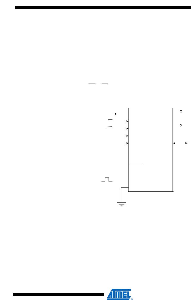
This section describes how to parallel program and verify Flash Program memory, EEPROM Data memory, Memory Lock bits, and Fuse bits in the Atmel® AVR®ATmega128. Pulses are assumed to be at least 250ns unless otherwise noted.
In this section, some pins of the ATmega128 are referenced by signal names describing their functionality during parallel programming, see Figure 135 and Table 120. Pins not described in the following table are referenced by pin names.
The XA1/XA0 pins determine the action executed when the XTAL1 pin is given a positive pulse. The bit coding is shown in Table 122.
When pulsing WR or OE, the command loaded determines the action executed. The different Commands are shown in Table 123.
Figure 135. Parallel Programming
|
|
|
|
|
|
|
|
|
|
|
|
+5V |
||
|
|
|
|
|
|
|
|
|
|
|
||||
|
|
|
|
|
|
|
|
|
|
|
|
|
|
|
RDY/BSY |
|
|
|
|
PD1 |
VCC |
|
|
|
|
|
|||
|
OE |
|
|
|
|
PD2 |
|
|
|
|
|
|||
|
|
|
|
|
|
|
+5V |
|||||||
|
|
|
|
|
|
|
|
|||||||
|
|
|
|
|
|
|||||||||
|
|
|
|
|
|
|
|
|
|
|
|
|||
|
WR |
|
|
|
PD3 |
AVCC |
|
|
|
|
|
|
||
|
|
|
|
|
|
|
|
|
|
|
||||
|
|
|
|
|
|
|
|
|||||||
|
BS1 |
|
|
|
|
PD4 |
|
|
|
|
|
|||
|
|
|
|
|
|
|
|
|
|
|
||||
|
|
|
|
|
|
|
|
|
||||||
|
XA0 |
|
|
|
PD5 |
PB7 - PB0 |
|
|
|
DATA |
||||
|
|
|
|
|
||||||||||
XA1  PD6
PD6
PAGEL  PD7
PD7
+12 V  RESET
RESET
BS2  PA0
PA0
 XTAL1
XTAL1
GND
Table 120. Pin Name Mapping
|
Signal Name in |
|
|
|
||||
|
Programming Mode |
Pin Name |
I/O |
Function |
||||
|
|
|
|
|
|
|
|
|
|
|
|
|
|
|
|
|
0: Device is busy programming, 1: Device is ready for new |
|
RDY/BSY |
|
PD1 |
O |
||||
|
|
|
|
|
|
command |
||
|
|
|
|
|
|
|
|
|
|
|
|
|
|
|
|
||
|
|
|
|
PD2 |
I |
Output Enable (Active low) |
||
|
OE |
|||||||
|
|
|
|
|
|
|||
|
|
|
|
PD3 |
I |
Write Pulse (Active low) |
||
|
WR |
|||||||
|
|
|
|
|
||||
|
BS1 |
PD4 |
I |
Byte Select 1 (“0” selects low byte, “1” selects high byte) |
||||
|
|
|
|
|
||||
|
XA0 |
PD5 |
I |
XTAL Action Bit 0 |
||||
|
|
|
|
|
||||
|
XA1 |
PD6 |
I |
XTAL Action Bit 1 |
||||
|
|
|
|
|
|
|
|
|
290
2467X–AVR–06/11
|
|
|
|
|
|
ATmega128 |
||
|
|
|
|
|
|
|||
|
|
|
|
|
|
|||
|
|
Table 120. Pin Name Mapping (Continued) |
||||||
|
|
|||||||
|
|
|
|
|
|
|
|
|
|
|
Signal Name in |
|
|
|
|
|
|
|
|
Programming Mode |
Pin Name |
I/O |
Function |
|||
|
|
|
|
|
|
|||
|
|
PAGEL |
PD7 |
I |
Program Memory and EEPROM data Page Load |
|||
|
|
|
|
|
|
|||
|
|
BS2 |
PA0 |
I |
Byte Select 2 (“0” selects low byte, “1” selects 2’nd high |
|||
|
|
|
byte) |
|||||
|
|
|
|
|
||||
|
|
|
|
|
|
|
|
|
|
|
DATA |
PB7-0 |
I/O |
Bi-directional Data bus (Output when |
|
is low) |
|
|
OE |
|||||||
|
|
|
|
|
|
|
|
|
Table 121. Pin Values Used to Enter Programming Mode
Pin |
Symbol |
Value |
|
|
|
PAGEL |
Prog_enable[3] |
0 |
|
|
|
XA1 |
Prog_enable[2] |
0 |
|
|
|
XA0 |
Prog_enable[1] |
0 |
|
|
|
BS1 |
Prog_enable[0] |
0 |
|
|
|
Table 122. XA1 and XA0 Coding
XA1 |
XA0 |
Action when XTAL1 is Pulsed |
|
|
|
0 |
0 |
Load Flash or EEPROM Address (High or low address byte determined by BS1) |
|
|
|
0 |
1 |
Load Data (High or Low data byte for Flash determined by BS1) |
|
|
|
1 |
0 |
Load Command |
|
|
|
1 |
1 |
No Action, Idle |
|
|
|
Table 123. Command Byte Bit Coding
Command Byte |
Command Executed |
|
|
1000 0000 |
Chip Erase |
|
|
0100 0000 |
Write Fuse bits |
|
|
0010 0000 |
Write Lock bits |
|
|
0001 0000 |
Write Flash |
|
|
0001 0001 |
Write EEPROM |
|
|
0000 1000 |
Read Signature Bytes and Calibration byte |
|
|
0000 0100 |
Read Fuse and Lock bits |
|
|
0000 0010 |
Read Flash |
|
|
0000 0011 |
Read EEPROM |
|
|
Table 124. No. of Words in a Page and no. of Pages in the Flash
Flash Size |
Page Size |
PCWORD |
No. of Pages |
PCPAGE |
PCMSB |
|
|
|
|
|
|
64K words (128 Kbytes) |
128 words |
PC[6:0] |
512 |
PC[15:7] |
15 |
|
|
|
|
|
|
291
2467X–AVR–06/11

 ATmega128
Table 125. No. of Words in a Page and no. of Pages in the EEPROM
EEPROM Size |
Page Size |
PCWORD |
No. of Pages |
PCPAGE |
EEAMSB |
|
|
|
|
|
|
4 Kbytes |
8 bytes |
EEA[2:0] |
512 |
EEA[11:3] |
8 |
|
|
|
|
|
|
Parallel
Programming
Enter Programming |
The following algorithm puts the device in parallel programming mode: |
|||||||
Mode |
1. |
Apply 4.5V - 5.5V between VCC and GND, and wait at least 100µs. |
||||||
|
||||||||
|
2. |
Set |
|
to “0” and toggle XTAL1 at least SIX times. |
||||
|
RESET |
|||||||
|
3. |
Set the Prog_enable pins listed in Table 121 on page 291 to “0000” and wait at least |
||||||
|
|
100ns. |
||||||
|
4. |
Apply 11.5 - 12.5V to |
|
|
Any activity on Prog_enable pins within 100ns after +12V |
|||
|
RESET. |
|||||||
|
|
has been applied to |
RESET, |
will cause the device to fail entering programming mode. |
||||
Note, if External Crystal or External RC configuration is selected, it may not be possible to apply qualified XTAL1 pulses. In such cases, the following algorithm should be followed:
1.Set Prog_enable pins listed in Table on page 291 to “0000”.
2.Apply 4.5 - 5.5V between VCC and GND simultaneously as 11.5 - 12.5V is applied to RESET.
3.Wait 100 µs.
4.Re-program the fuses to ensure that External Clock is selected as clock source (CKSEL3:0 = 0b0000) If Lock bits are programmed, a Chip Erase command must be executed before changing the fuses.
5.Exit Programming mode by power the device down or by bringing RESET pin to 0b0.
6.Entering Programming mode with the original algorithm, as described above.
Considerations for The loaded command and address are retained in the device during programming. For efficient Efficient Programming programming, the following should be considered.
•The command needs only be loaded once when writing or reading multiple memory locations.
•Skip writing the data value $FF, that is the contents of the entire EEPROM (unless the EESAVE fuse is programmed) and Flash after a Chip Erase.
•Address high byte needs only be loaded before programming or reading a new 256 word window in Flash or 256-byte EEPROM. This consideration also applies to Signature bytes reading.
Chip Erase |
The Chip Erase will erase the Flash and EEPROM(1) memories plus Lock bits. The Lock bits are |
|
not reset until the program memory has been completely erased. The Fuse bits are not |
|
changed. A Chip Erase must be performed before the Flash and/or the EEPROM are |
|
reprogrammed. |
|
Note: 1. The EEPRPOM memory is preserved during chip erase if the EESAVE fuse is programmed. |
Load Command “Chip Erase”
1.Set XA1, XA0 to “10”. This enables command loading.
2.Set BS1 to “0”.
3.Set DATA to “1000 0000”. This is the command for Chip Erase.
4.Give XTAL1 a positive pulse. This loads the command.
292
2467X–AVR–06/11

 ATmega128
5.Give WR a negative pulse. This starts the Chip Erase. RDY/BSY goes low.
6.Wait until RDY/BSY goes high before loading a new command.
Programming the The Flash is organized in pages, see Table 123 on page 291. When programming the Flash, the Flash program data is latched into a page buffer. This allows one page of program data to be programmed simultaneously. The following procedure describes how to program the entire Flash
memory:
A. Load Command “Write Flash”
1.Set XA1, XA0 to “10”. This enables command loading.
2.Set BS1 to “0”.
3.Set DATA to “0001 0000”. This is the command for Write Flash.
4.Give XTAL1 a positive pulse. This loads the command.
B. Load Address Low byte
1.Set XA1, XA0 to “00”. This enables address loading.
2.Set BS1 to “0”. This selects low address.
3.Set DATA = Address low byte ($00 - $FF).
4.Give XTAL1 a positive pulse. This loads the address low byte.
C. Load Data Low Byte
1.Set XA1, XA0 to “01”. This enables data loading.
2.Set DATA = Data low byte ($00 - $FF).
3.Give XTAL1 a positive pulse. This loads the data byte.
D. Load Data High Byte
1.Set BS1 to “1”. This selects high data byte.
2.Set XA1, XA0 to “01”. This enables data loading.
3.Set DATA = Data high byte ($00 - $FF).
4.Give XTAL1 a positive pulse. This loads the data byte.
E. Latch Data
1.Set BS1 to “1”. This selects high data byte.
2.Give PAGEL a positive pulse. This latches the data bytes. (See Figure 137 for signal waveforms)
F. Repeat B through E until the entire buffer is filled or until all data within the page is loaded.
While the lower bits in the address are mapped to words within the page, the higher bits address the pages within the FLASH. This is illustrated in Figure 136 on page 294. Note that if less than 8 bits are required to address words in the page (pagesize < 256), the most significant bit(s) in the address low byte are used to address the page when performing a page write.
G. Load Address High byte
1.Set XA1, XA0 to “00”. This enables address loading.
2.Set BS1 to “1”. This selects high address.
3.Set DATA = Address high byte ($00 - $FF).
4.Give XTAL1 a positive pulse. This loads the address high byte.
H. Program Page
293
2467X–AVR–06/11

 ATmega128
1.Set BS1 = “0”
2.Give WR a negative pulse. This starts programming of the entire page of data. RDY/BSY goes low.
3.Wait until RDY/BSY goes high. (See Figure 137 for signal waveforms)
I.Repeat B through H until the entire Flash is programmed or until all data has been programmed.
J.End Page Programming
1.1. Set XA1, XA0 to “10”. This enables command loading.
2.Set DATA to “0000 0000”. This is the command for No Operation.
3.Give XTAL1 a positive pulse. This loads the command, and the internal write signals are reset.
Figure 136. Addressing the Flash which is Organized in Pages
|
PROGRAM |
PCMSB |
|
|
|
|
PAGEMSB |
|
|||||||
|
|
PCPAGE |
PCWORD |
|
|
|
|
||||||||
|
COUNTER |
|
|
|
|
|
|||||||||
|
|
|
|
|
|
|
|
|
|
|
|
|
|
||
|
PAGE ADDRESS |
|
|
WORD ADDRESS |
|
||||||||||
|
WITHIN THE FLASH |
|
|
WITHIN A PAGE |
|
||||||||||
PROGRAM MEMORY |
|
|
|
|
|
|
|
|
|
PAGE |
PCWORD[PAGEMSB:0]: |
||||
|
|
|
|
|
|
|
|
|
|
|
|
|
|
|
|
|
PAGE |
|
|
|
|
|
|
|
|
INSTRUCTION WORD |
00 |
||||
|
|
|
|
|
|
|
|
|
|
|
|
||||
|
|
|
|
|
|
|
|
|
|
|
|
|
|
|
01 |
|
|
|
|
|
|
|
|
|
|
|
|
|
|
|
|
|
|
|
|
|
|
|
|
|
|
|
|
|
|
|
02 |
|
|
|
|
|
|
|
|
|
|
|
|
|
|
|
|
|
|
|
|
|
|
|
|
|
|
|
|
|
|
|
|
|
|
|
|
|
|
|
|
|
|
|
|
|
|
|
|
|
|
|
|
|
|
|
|
|
|
|
|
|
|
|
|
|
|
|
|
|
|
|
|
|
|
|
|
|
|
|
|
|
|
|
|
|
|
|
|
|
|
|
|
|
|
|
|
|
|
|
|
|
|
|
|
|
|
|
|
|
|
|
|
|
|
|
|
|
|
|
|
|
|
|
|
|
|
|
|
|
|
|
|
|
|
|
|
|
|
|
|
|
|
|
|
|
|
|
|
|
|
|
|
|
|
|
|
|
|
|
|
|
|
|
|
|
|
|
|
|
|
|
|
|
|
|
|
|
|
|
|
|
|
|
|
|
|
|
|
|
|
|
|
|
|
|
|
|
|
|
|
|
|
|
|
|
|
|
|
|
|
|
|
|
|
|
|
|
|
|
|
|
|
|
|
PAGEEND
Note: 1. PCPAGE and PCWORD are listed in Table 124 on page 291.
294
2467X–AVR–06/11

 ATmega128
Figure 137. Programming the Flash Waveforms
|
|
|
|
|
|
|
|
|
F |
|
|
|
|
|
A |
B |
C |
D |
E |
B |
C |
D |
E |
G |
H |
|
DATA |
0x10 |
ADDR. LOW |
DATA LOW |
DATA HIGH |
XX |
ADDR. LOW |
DATA LOW |
DATA HIGH |
XX |
ADDR. HIGH |
XX |
|
|
|
|
|
|
|
|
|
|
|
|
|
|
XA1 |
|
|
|
|
|
|
|
|
|
|
|
|
XA0 |
|
|
|
|
|
|
|
|
|
|
|
|
BS1 |
|
|
|
|
|
|
|
|
|
|
|
|
XTAL1 |
|
|
|
|
|
|
|
|
|
|
|
|
WR |
|
|
|
|
|
|
|
|
|
|
|
|
RDY/BSY |
|
|
|
|
|
|
|
|
|
|
|
|
RESET +12V |
|
|
|
|
|
|
|
|
|
|
|
|
OE |
|
|
|
|
|
|
|
|
|
|
|
|
PAGEL |
|
|
|
|
|
|
|
|
|
|
|
|
BS2 |
|
|
|
|
|
|
|
|
|
|
|
Note: |
“XX” is don’t care. The letters refer to the programming description above. |
|||||||||||
Programming the The EEPROM is organized in pages, see Table 124 on page 291. When programming the EEPROM EEPROM, the program data is latched into a page buffer. This allows one page of data to be programmed simultaneously. The programming algorithm for the EEPROM data memory is as follows (refer to “Programming the Flash” on page 293 for details on Command, Address and
Data loading):
1.A: Load Command “0001 0001”.
2.G: Load Address High Byte ($00 - $FF).
3.B: Load Address Low Byte ($00 - $FF).
4.C: Load Data ($00 - $FF).
5.E: Latch data (give PAGEL a positive pulse).
K:Repeat 3 through 5 until the entire buffer is filled.
L:Program EEPROM page:
1.Set BS1 to “0”.
2.Give WR a negative pulse. This starts programming of the EEPROM page. RDY/BSY goes low.
3.Wait until to RDY/BSY goes high before programming the next page. (See Figure 138 for signal waveforms.)
295
2467X–AVR–06/11