

 ATmega128
Unconnected pins
Alternate Port
Functions
If some pins are unused, it is recommended to ensure that these pins have a defined level. Even though most of the digital inputs are disabled in the deep sleep modes as described above, floating inputs should be avoided to reduce current consumption in all other modes where the digital inputs are enabled (Reset, Active mode and Idle mode).
The simplest method to ensure a defined level of an unused pin, is to enable the internal pull-up. In this case, the pull-up will be disabled during reset. If low power consumption during reset is important, it is recommended to use an external pull-up or pull-down. Connecting unused pins directly to VCC or GND is not recommended, since this may cause excessive currents if the pin is accidentally configured as an output.
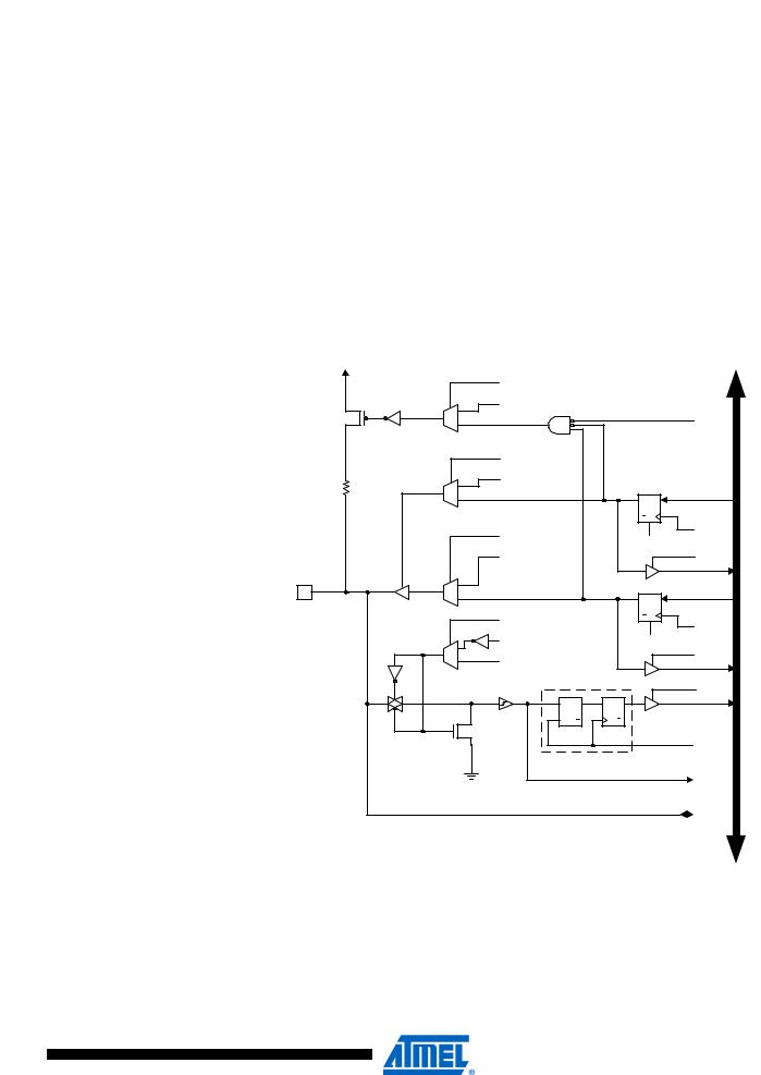
Most port pins have alternate functions in addition to being general digital I/Os. Figure 33 shows how the port pin control signals from the simplified Figure 30 can be overridden by alternate functions. The overriding signals may not be present in all port pins, but the figure serves as a generic description applicable to all port pins in the AVR microcontroller family.
Figure 33. Alternate Port Functions(1) |
|
|
|
|
|
|
|
|
PUOExn |
|
|
|
|
|
|
1 |
PUOVxn |
|
|
|
|
|
|
|
|
|
|
|
|
|
|
0 |
|
|
|
|
|
PUD |
|
|
|
|
|
|
|
|
|
|
DDOExn |
|
|
|
|
|
|
1 |
DDOVxn |
|
|
|
|
|
|
|
|
|
|
|
|
|
|
0 |
|
|
|
Q |
D |
|
|
|
|
|
|
DDxn |
|
|
|
|
|
|
|
Q CLR |
|
|
|
|
PVOExn |
|
|
|
|
WDx |
|
|
|
|
RESET |
|
|
||
|
|
|
|
|
|
||
|
PVOVxn |
|
|
|
|
RDx |
BUS |
1 |
|
|
|
|
|
|
|
Pxn |
|
|
|
Q |
D |
|
DATA |
0 |
|
|
|
|
|||
|
|
|
|
|
|||
|
|
|
|
PORTxn |
|
|
|
|
DIEOExn |
|
|
Q CLR |
|
|
|
|
|
|
|
|
|
|
|
|
|
|
|
|
|
WPx |
|
1 |
DIEOVxn |
|
|
RESET |
|
|
|
|
|
|
|
|
RRx |
|
|
0 |
SLEEP |
|
|
|
|
|
|
|
|
|
|
|
|
||
|
SYNCHRONIZER |
|
RPx |
|
|||
|
|
|
|
|
|
|
|
|
D SET |
Q |
D |
Q |
|
|
|
|
|
|
PINxn |
|
|
|
|
|
L CLR |
Q |
|
CLR Q |
|
|
|
|
|
|
|
|
|
clk I/O |
|
|
|
|
|
|
|
DIxn |
|
|
|
|
|
|
|
AIOxn |
|
PUOExn: |
Pxn PULL-UP OVERRIDE ENABLE |
PUD: |
PULLUP DISABLE |
PUOVxn: |
Pxn PULL-UP OVERRIDE VALUE |
WDx: |
WRITE DDRx |
DDOExn: |
Pxn DATA DIRECTION OVERRIDE ENABLE |
RDx: |
READ DDRx |
DDOVxn: |
Pxn DATA DIRECTION OVERRIDE VALUE |
RRx: |
READ PORTx REGISTER |
PVOExn: |
Pxn PORT VALUE OVERRIDE ENABLE |
WPx: |
WRITE PORTx |
PVOVxn: |
Pxn PORT VALUE OVERRIDE VALUE |
RPx: |
READ PORTx PIN |
DIEOExn: Pxn DIGITAL INPUT-ENABLE OVERRIDE ENABLE |
clk : |
I/O CLOCK |
|
DIEOVxn: Pxn DIGITAL INPUT-ENABLE OVERRIDE VALUE |
I/O |
DIGITAL INPUT PIN n ON PORTx |
|
DIxn: |
|||
SLEEP: |
SLEEP CONTROL |
AIOxn: |
ANALOG INPUT/OUTPUT PIN n ON PORTx |
Note: 1. WPx, WDx, RLx, RPx, and RDx are common to all pins within the same port. clkI/O, SLEEP, and PUD are common to all ports. All other signals are unique for each pin.
70
2467X–AVR–06/11
 ATmega128
Table 26 summarizes the function of the overriding signals. The pin and port indexes from Figure 33 are not shown in the succeeding tables. The overriding signals are generated internally in the modules having the alternate function.
Table 26. Generic Description of Overriding Signals for Alternate Functions.
Signal |
|
|
Name |
Full Name |
Description |
|
|
|
PUOE |
Pull-up |
If this signal is set, the pull-up enable is controlled by the |
|
Override Enable |
PUOV signal. If this signal is cleared, the pull-up is |
|
|
enabled when {DDxn, PORTxn, PUD} = 0b010. |
|
|
|
PUOV |
Pull-up |
If PUOE is set, the pull-up is enabled/disabled when |
|
Override Value |
PUOV is set/cleared, regardless of the setting of the |
|
|
DDxn, PORTxn, and PUD Register bits. |
|
|
|
DDOE |
Data Direction |
If this signal is set, the Output Driver Enable is controlled |
|
Override Enable |
by the DDOV signal. If this signal is cleared, the Output |
|
|
driver is enabled by the DDxn Register bit. |
|
|
|
DDOV |
Data Direction |
If DDOE is set, the Output Driver is enabled/disabled |
|
Override Value |
when DDOV is set/cleared, regardless of the setting of the |
|
|
DDxn Register bit. |
|
|
|
PVOE |
Port Value |
If this signal is set and the Output Driver is enabled, the |
|
Override Enable |
port value is controlled by the PVOV signal. If PVOE is |
|
|
cleared, and the Output Driver is enabled, the port Value |
|
|
is controlled by the PORTxn Register bit. |
|
|
|
PVOV |
Port Value |
If PVOE is set, the port value is set to PVOV, regardless of |
|
Override Value |
the setting of the PORTxn Register bit. |
|
|
|
DIEOE |
Digital Input |
If this bit is set, the Digital Input Enable is controlled by the |
|
Enable Override |
DIEOV signal. If this signal is cleared, the Digital Input |
|
Enable |
Enable is determined by MCU-state (Normal mode, Sleep |
|
|
modes). |
|
|
|
DIEOV |
Digital Input |
If DIEOE is set, the Digital Input is enabled/disabled when |
|
Enable Override |
DIEOV is set/cleared, regardless of the MCU state |
|
Value |
(Normal mode, Sleep modes). |
|
|
|
DI |
Digital Input |
This is the Digital Input to alternate functions. In the |
|
|
figure, the signal is connected to the output of the schmitt |
|
|
trigger but before the synchronizer. Unless the Digital |
|
|
Input is used as a clock source, the module with the |
|
|
alternate function will use its own synchronizer. |
|
|
|
AIO |
Analog |
This is the Analog Input/output to/from alternate functions. |
|
Input/output |
The signal is connected directly to the pad, and can be |
|
|
used bi-directionally. |
|
|
|
The following subsections shortly describes the alternate functions for each port, and relates the overriding signals to the alternate function. Refer to the alternate function description for further details.
71
2467X–AVR–06/11

 ATmega128
Special Function IO
Register – SFIOR
Bit |
7 |
6 |
5 |
4 |
3 |
2 |
1 |
0 |
|
|
TSM |
– |
– |
– |
ACME |
PUD |
PSR0 |
PSR321 |
SFIOR |
Read/Write |
R/W |
R |
R |
R |
R/W |
R/W |
R/W |
R/W |
|
Initial Value |
0 |
0 |
0 |
0 |
0 |
0 |
0 |
0 |
|
• Bit 2 – PUD: Pull-up disable
When this bit is written to one, the pull-ups in the I/O ports are disabled even if the DDxn and PORTxn Registers are configured to enable the pull-ups ({DDxn, PORTxn} = 0b01). See “Configuring the Pin” on page 66 for more details about this feature.
Alternate Functions of The Port A has an alternate function as the address low byte and data lines for the External
Port A |
Memory Interface. |
|
|
|
|
|
|
|
|
|
|
|
|
|
|
|
|
|
|
|
|
|
|
|
|
|
|
|
|
|||||||||||
|
Table 27. Port A Pins Alternate Functions |
|
|
|
|
|
|
|
|
|
|
|
|
|
|
|
|
|
|
|
||||||||||||||||||||
|
|
|
|
|
|
|
|
|
|
|
|
|
|
|
|
|
|
|
|
|
|
|
|
|
||||||||||||||||
|
Port Pin |
|
Alternate Function |
|
|
|
|
|
|
|
|
|
|
|
|
|
|
|
|
|
|
|
||||||||||||||||||
|
|
|
|
|
|
|
|
|
|
|
|
|
|
|
|
|
|
|
|
|
||||||||||||||||||||
|
PA7 |
|
|
|
|
|
AD7 (External memory interface address and data bit 7) |
|
|
|
|
|
|
|
|
|
|
|||||||||||||||||||||||
|
|
|
|
|
|
|
|
|
|
|
|
|
|
|
|
|
|
|
|
|
||||||||||||||||||||
|
PA6 |
|
|
|
|
|
AD6 (External memory interface address and data bit 6) |
|
|
|
|
|
|
|
|
|
|
|||||||||||||||||||||||
|
|
|
|
|
|
|
|
|
|
|
|
|
|
|
|
|
|
|
|
|
||||||||||||||||||||
|
PA5 |
|
|
|
|
|
AD5 (External memory interface address and data bit 5) |
|
|
|
|
|
|
|
|
|
|
|||||||||||||||||||||||
|
|
|
|
|
|
|
|
|
|
|
|
|
|
|
|
|
|
|
|
|
||||||||||||||||||||
|
PA4 |
|
|
|
|
|
AD4 (External memory interface address and data bit 4) |
|
|
|
|
|
|
|
|
|
|
|||||||||||||||||||||||
|
|
|
|
|
|
|
|
|
|
|
|
|
|
|
|
|
|
|
|
|
||||||||||||||||||||
|
PA3 |
|
|
|
|
|
AD3 (External memory interface address and data bit 3) |
|
|
|
|
|
|
|
|
|
|
|||||||||||||||||||||||
|
|
|
|
|
|
|
|
|
|
|
|
|
|
|
|
|
|
|
|
|
||||||||||||||||||||
|
PA2 |
|
|
|
|
|
AD2 (External memory interface address and data bit 2) |
|
|
|
|
|
|
|
|
|
|
|||||||||||||||||||||||
|
|
|
|
|
|
|
|
|
|
|
|
|
|
|
|
|
|
|
|
|
||||||||||||||||||||
|
PA1 |
|
|
|
|
|
AD1 (External memory interface address and data bit 1) |
|
|
|
|
|
|
|
|
|
|
|||||||||||||||||||||||
|
|
|
|
|
|
|
|
|
|
|
|
|
|
|
|
|
|
|
|
|
||||||||||||||||||||
|
PA0 |
|
|
|
|
|
AD0 (External memory interface address and data bit 0) |
|
|
|
|
|
|
|
|
|
|
|||||||||||||||||||||||
|
|
|
|
|
|
|
|
|||||||||||||||||||||||||||||||||
|
Table 28 and Table 29 relates the alternate functions of Port A to the overriding signals shown in |
|||||||||||||||||||||||||||||||||||||||
|
Figure 33 on page 70. |
|
|
|
|
|
|
|
|
|
|
|
|
|
|
|
|
|
|
|
|
|
|
|
|
|
|
|
|
|||||||||||
|
Table 28. Overriding Signals for Alternate Functions in PA7..PA4 |
|
|
|
|
|
|
|
|
|
|
|||||||||||||||||||||||||||||
|
|
|
|
|
|
|
|
|
|
|
|
|
|
|
|
|
|
|
|
|
|
|
|
|
|
|
|
|
|
|
|
|
|
|
|
|
|
|
|
|
|
Signal |
|
|
|
|
|
|
|
|
|
|
|
|
|
|
|
|
|
|
|
|
|
|
|
|
|
|
|
|
|
|
|
|
|
|
|
|
|
|
|
|
Name |
|
|
PA7/AD7 |
PA6/AD6 |
PA5/AD5 |
PA4/AD4 |
|
||||||||||||||||||||||||||||||||
|
|
|
|
|
|
|
|
|
|
|
|
|
|
|
|
|||||||||||||||||||||||||
|
PUOE |
|
|
SRE |
|
|
|
|
|
|
SRE |
SRE |
|
SRE |
|
|||||||||||||||||||||||||
|
|
|
|
|
|
|
|
|
|
|
|
|
|
|
|
|
|
|
|
|
||||||||||||||||||||
|
PUOV |
|
~( |
|
|
|
| ADA(1)) • |
~( |
|
|
| ADA) • |
~( |
|
|
| ADA) • |
~( |
|
|
| ADA) • |
|
||||||||||||||||||||
|
WR |
WR |
WR |
WR |
||||||||||||||||||||||||||||||||||||
|
|
|
|
PORTA7 • |
PUD |
|
|
PORTA6 • |
PUD |
|
|
PORTA5 • |
PUD |
|
|
PORTA4 • |
PUD |
|
|
|||||||||||||||||||||
|
|
|
|
|
|
|
|
|
|
|
|
|
||||||||||||||||||||||||||||
|
DDOE |
|
SRE |
|
|
|
|
|
SRE |
SRE |
SRE |
|
||||||||||||||||||||||||||||
|
|
|
|
|
|
|
|
|
|
|
|
|
|
|
|
|||||||||||||||||||||||||
|
DDOV |
|
|
|
|
| ADA |
|
|
|
| ADA |
|
|
|
| ADA |
|
|
|
| ADA |
|
|||||||||||||||||||||
|
|
WR |
WR |
WR |
WR |
|||||||||||||||||||||||||||||||||||
|
|
|
|
|
|
|
|
|
|
|
|
|
|
|
||||||||||||||||||||||||||
|
PVOE |
|
|
SRE |
|
|
|
|
|
|
SRE |
SRE |
SRE |
|
||||||||||||||||||||||||||
|
|
|
|
|
|
|
|
|
|
|
|
|||||||||||||||||||||||||||||
|
PVOV |
|
|
A7 • ADA | D7 |
|
A6 • ADA | D6 |
|
A5 • ADA | D5 |
|
A4 • ADA | D4 |
|
|||||||||||||||||||||||||||||
|
|
|
|
OUTPUT • |
WR |
|
|
OUTPUT • |
WR |
|
|
OUTPUT • |
WR |
|
|
OUTPUT • |
WR |
|
|
|||||||||||||||||||||
|
|
|
|
|
|
|
|
|
|
|
|
|
|
|
|
|
|
|
|
|
|
|
|
|
|
|
|
|
|
|
|
|
|
|
|
|
||||
|
DIEOE |
|
0 |
|
|
|
|
|
|
|
|
0 |
|
|
|
|
|
|
|
0 |
|
|
|
|
|
|
|
0 |
|
|
|
|
|
|
|
|
||||
|
|
|
|
|
|
|
|
|
|
|
|
|
|
|
|
|
|
|
|
|
|
|
|
|
|
|
|
|
|
|
|
|
|
|
|
|
||||
|
DIEOV |
|
0 |
|
|
|
|
|
|
|
|
0 |
|
|
|
|
|
|
|
0 |
|
|
|
|
|
|
|
0 |
|
|
|
|
|
|
|
|
||||
|
|
|
|
|
|
|
|
|
|
|
|
|||||||||||||||||||||||||||||
|
DI |
|
|
D7 INPUT |
|
D6 INPUT |
|
D5 INPUT |
|
D4 INPUT |
|
|||||||||||||||||||||||||||||
|
|
|
|
|
|
|
|
|
|
|
|
|
|
|
|
|
||||||||||||||||||||||||
|
AIO |
|
|
– |
|
|
|
|
|
|
– |
|
– |
|
– |
|
||||||||||||||||||||||||
|
|
|
|
|
|
|
|
|
|
|
|
|
|
|
|
|
|
|
|
|
|
|
|
|
|
|
|
|
|
|
|
|
|
|
|
|
|
|
|
|
Note: 1. ADA is short for ADdress Active and represents the time when address is output. See “External Memory Interface” on page 25 for details.
72
2467X–AVR–06/11

 ATmega128
Table 29. Overriding Signals for Alternate Functions in PA3..PA0
Signal |
|
|
|
|
|
|
|
|
|
|
|
|
|
|
|
|
|
|
|
|
|
|
|
|
|
|
|
|
|
|
|
|
|
|
|
|
Name |
|
PA3/AD3 |
|
PA2/AD2 |
|
PA1/AD1 |
PA0/AD0 |
|||||||||||||||||||||||||||||
|
|
|
|
|
|
|
|
|||||||||||||||||||||||||||||
PUOE |
|
SRE |
|
SRE |
SRE |
|
SRE |
|||||||||||||||||||||||||||||
|
|
|
|
|
|
|
|
|
|
|
|
|
|
|
|
|
||||||||||||||||||||
PUOV |
~( |
|
|
| ADA) • |
~( |
|
|
| ADA) • |
~( |
|
|
| ADA) • |
~( |
|
|
| ADA) • |
||||||||||||||||||||
WR |
WR |
WR |
WR |
|||||||||||||||||||||||||||||||||
|
|
PORTA3 • |
PUD |
|
|
PORTA2 • |
PUD |
|
|
PORTA1 • |
PUD |
|
|
PORTA0 • |
PUD |
|
||||||||||||||||||||
|
|
|
|
|
||||||||||||||||||||||||||||||||
DDOE |
SRE |
SRE |
SRE |
SRE |
||||||||||||||||||||||||||||||||
|
|
|
|
|
|
|
|
|
|
|
|
|
||||||||||||||||||||||||
DDOV |
|
|
|
| ADA |
|
|
|
| ADA |
|
|
|
| ADA |
|
|
|
| ADA |
||||||||||||||||||||
|
WR |
WR |
WR |
WR |
||||||||||||||||||||||||||||||||
|
|
|
|
|
|
|
||||||||||||||||||||||||||||||
PVOE |
|
SRE |
|
SRE |
SRE |
SRE |
||||||||||||||||||||||||||||||
|
|
|
|
|
|
|
|
|
||||||||||||||||||||||||||||
PVOV |
|
A3 • ADA | D3 |
|
A2• ADA | D2 |
|
A1 • ADA | D1 |
|
A0 • ADA | D0 |
||||||||||||||||||||||||||||
|
|
OUTPUT • |
WR |
|
|
OUTPUT • |
WR |
|
|
OUTPUT • |
WR |
|
|
OUTPUT • |
WR |
|
||||||||||||||||||||
|
|
|
|
|
|
|
|
|
|
|
|
|
|
|
|
|
|
|
|
|
|
|
|
|
|
|
|
|
|
|
|
|
||||
DIEOE |
0 |
|
|
|
|
|
|
|
0 |
|
|
|
|
|
|
|
0 |
|
|
|
|
|
|
|
0 |
|
|
|
|
|
|
|
||||
|
|
|
|
|
|
|
|
|
|
|
|
|
|
|
|
|
|
|
|
|
|
|
|
|
|
|
|
|
|
|
|
|
||||
DIEOV |
0 |
|
|
|
|
|
|
|
0 |
|
|
|
|
|
|
|
0 |
|
|
|
|
|
|
|
0 |
|
|
|
|
|
|
|
||||
|
|
|
|
|
|
|
|
|
||||||||||||||||||||||||||||
DI |
|
D3 INPUT |
|
D2 INPUT |
|
D1 INPUT |
|
D0 INPUT |
||||||||||||||||||||||||||||
|
|
|
|
|
|
|
|
|
||||||||||||||||||||||||||||
AIO |
|
– |
|
– |
|
– |
|
– |
||||||||||||||||||||||||||||
|
|
|
|
|
|
|
|
|
|
|
|
|
|
|
|
|
|
|
|
|
|
|
|
|
|
|
|
|
|
|
|
|
|
|
|
|
Alternate Functions of The Port B pins with alternate functions are shown in Table 30.
Port B
Table 30. Port B Pins Alternate Functions
Port Pin |
Alternate Functions |
||
|
|
|
|
PB7 |
|
OC2/OC1C(1) (Output Compare and PWM Output for Timer/Counter2 or Output |
|
|
Compare and PWM Output C for Timer/Counter1) |
||
|
|
||
|
|
||
PB6 |
OC1B (Output Compare and PWM Output B for Timer/Counter1) |
||
|
|
||
PB5 |
OC1A (Output Compare and PWM Output A for Timer/Counter1) |
||
|
|
||
PB4 |
OC0 (Output Compare and PWM Output for Timer/Counter0) |
||
|
|
|
|
PB3 |
|
MISO (SPI Bus Master Input/Slave Output) |
|
|
|
|
|
PB2 |
|
MOSI (SPI Bus Master Output/Slave Input) |
|
|
|
|
|
PB1 |
|
SCK (SPI Bus Serial Clock) |
|
|
|
|
|
PB0 |
|
|
(SPI Slave Select input) |
|
SS |
||
|
|
||
Note: 1. |
OC1C not applicable in ATmega103 compatibility mode. |
||
The alternate pin configuration is as follows:
• OC2/OC1C, Bit 7
OC2, Output Compare Match output: The PB7 pin can serve as an external output for the Timer/Counter2 Output Compare. The pin has to be configured as an output (DDB7 set “one”) to serve this function. The OC2 pin is also the output pin for the PWM mode timer function.
OC1C, Output Compare Match C output: The PB7 pin can serve as an external output for the Timer/Counter1 Output Compare C. The pin has to be configured as an output (DDB7 set (one)) to serve this function. The OC1C pin is also the output pin for the PWM mode timer function.
73
2467X–AVR–06/11

 ATmega128
• OC1B, Bit 6
OC1B, Output Compare Match B output: The PB6 pin can serve as an external output for the Timer/Counter1 Output Compare B. The pin has to be configured as an output (DDB6 set (one)) to serve this function. The OC1B pin is also the output pin for the PWM mode timer function.
• OC1A, Bit 5
OC1A, Output Compare Match A output: The PB5 pin can serve as an external output for the Timer/Counter1 Output Compare A. The pin has to be configured as an output (DDB5 set (one)) to serve this function. The OC1A pin is also the output pin for the PWM mode timer function.
• OC0, Bit 4
OC0, Output Compare Match output: The PB4 pin can serve as an external output for the Timer/Counter0 Output Compare. The pin has to be configured as an output (DDB4 set (one)) to serve this function. The OC0 pin is also the output pin for the PWM mode timer function.
• MISO – Port B, Bit 3
MISO: Master Data input, Slave Data output pin for SPI channel. When the SPI is enabled as a master, this pin is configured as an input regardless of the setting of DDB3. When the SPI is enabled as a slave, the data direction of this pin is controlled by DDB3. When the pin is forced to be an input, the pull-up can still be controlled by the PORTB3 bit.
• MOSI – Port B, Bit 2
MOSI: SPI Master Data output, Slave Data input for SPI channel. When the SPI is enabled as a slave, this pin is configured as an input regardless of the setting of DDB2. When the SPI is enabled as a master, the data direction of this pin is controlled by DDB2. When the pin is forced to be an input, the pull-up can still be controlled by the PORTB2 bit.
• SCK – Port B, Bit 1
SCK: Master Clock output, Slave Clock input pin for SPI channel. When the SPI is enabled as a slave, this pin is configured as an input regardless of the setting of DDB1. When the SPI is enabled as a master, the data direction of this pin is controlled by DDB1. When the pin is forced to be an input, the pull-up can still be controlled by the PORTB1 bit.
• SS – Port B, Bit 0
SS: Slave Port Select input. When the SPI is enabled as a slave, this pin is configured as an input regardless of the setting of DDB0. As a slave, the SPI is activated when this pin is driven low. When the SPI is enabled as a master, the data direction of this pin is controlled by DDB0. When the pin is forced to be an input, the pull-up can still be controlled by the PORTB0 bit.
Table 31 and Table 32 relate the alternate functions of Port B to the overriding signals shown in Figure 33 on page 70. SPI MSTR INPUT and SPI SLAVE OUTPUT constitute the MISO signal, while MOSI is divided into SPI MSTR OUTPUT and SPI SLAVE INPUT.
74
2467X–AVR–06/11

 ATmega128
Table 31. Overriding Signals for Alternate Functions in PB7..PB4
Signal Name |
PB7/OC2/OC1C |
PB6/OC1B |
PB5/OC1A |
PB4/OC0 |
|
|
|
|
|
PUOE |
0 |
0 |
0 |
0 |
|
|
|
|
|
PUOV |
0 |
0 |
0 |
0 |
|
|
|
|
|
DDOE |
0 |
0 |
0 |
0 |
|
|
|
|
|
DDOV |
0 |
0 |
0 |
0 |
|
|
|
|
|
PVOE |
OC2/OC1C ENABLE(1) |
OC1B ENABLE |
OC1A ENABLE |
OC0 ENABLE |
PVOV |
OC2/OC1C(1) |
OC1B |
OC1A |
OC0B |
DIEOE |
0 |
0 |
0 |
0 |
|
|
|
|
|
DIEOV |
0 |
0 |
0 |
0 |
|
|
|
|
|
DI |
– |
– |
– |
– |
|
|
|
|
|
AIO |
– |
– |
– |
– |
|
|
|
|
|
Note: 1. See “Output Compare Modulator (OCM1C2)” on page 160 for details. OC1C does not exist in ATmega103 compatibility mode.
Table 32. Overriding Signals for Alternate Functions in PB3..PB0
Signal |
|
|
|
|
|
|
|
|
|
|
|
|
|
|
|
|
|
|
|
|
|
|
|
|
|
Name |
PB3/MISO |
PB2/MOSI |
PB1/SCK |
|
|
|
|
|
|
|
|
|
|||||||||||||
PB0/SS |
|
|
|
|
|||||||||||||||||||||
|
|
|
|
|
|
|
|
|
|
|
|
|
|
|
|
|
|
|
|||||||
PUOE |
SPE • MSTR |
SPE • |
|
|
|
|
|
SPE • |
|
|
|
|
SPE • |
|
|
|
|
|
|
||||||
MSTR |
MSTR |
MSTR |
|||||||||||||||||||||||
|
|
|
|
|
|
|
|
|
|
|
|
|
|
|
|||||||||||
PUOV |
PORTB3 • |
|
|
|
PORTB2 • |
|
|
|
|
PORTB1 • |
|
|
|
PORTB0 • |
|
|
|
||||||||
PUD |
PUD |
PUD |
PUD |
||||||||||||||||||||||
|
|
|
|
|
|
|
|
|
|
|
|
||||||||||||||
DDOE |
SPE • MSTR |
SPE • |
|
|
|
|
SPE • |
|
|
|
SPE • |
|
|
|
|
|
|||||||||
MSTR |
MSTR |
MSTR |
|||||||||||||||||||||||
|
|
|
|
|
|
|
|
|
|
|
|
|
|
|
|
|
|
|
|
|
|
|
|
|
|
DDOV |
0 |
|
|
|
|
0 |
|
|
|
|
|
0 |
|
|
|
|
0 |
|
|
|
|
|
|
|
|
|
|
|
|
|
|
|
|
|
|
|
|
|
|
|
|||||||||||
PVOE |
SPE • |
|
|
|
SPE • MSTR |
SPE • MSTR |
0 |
|
|
|
|
|
|
|
|
||||||||||
MSTR |
|
|
|
|
|
|
|
||||||||||||||||||
|
|
|
|
|
|
|
|
|
|
|
|
|
|||||||||||||
PVOV |
SPI SLAVE OUTPUT |
SPI MSTR OUTPUT |
SCK OUTPUT |
0 |
|
|
|
|
|
|
|
|
|||||||||||||
|
|
|
|
|
|
|
|
|
|
|
|
|
|
|
|
|
|
|
|
|
|
|
|
|
|
DIEOE |
0 |
|
|
|
|
0 |
|
|
|
|
|
0 |
|
|
|
|
0 |
|
|
|
|
|
|
|
|
|
|
|
|
|
|
|
|
|
|
|
|
|
|
|
|
|
|
|
|
|
|
|
|
|
|
DIEOV |
0 |
|
|
|
|
0 |
|
|
|
|
|
0 |
|
|
|
|
0 |
|
|
|
|
|
|
|
|
|
|
|
|
|
|
|
|||||||||||||||||||
DI |
SPI MSTR INPUT |
SPI SLAVE INPUT |
SCK INPUT |
SPI |
|
|
|
|
|||||||||||||||||
SS |
|||||||||||||||||||||||||
|
|
|
|
|
|||||||||||||||||||||
AIO |
– |
– |
– |
– |
|||||||||||||||||||||
|
|
|
|
|
|
|
|
|
|
|
|
|
|
|
|
|
|
|
|
|
|
|
|
|
|
75
2467X–AVR–06/11

 ATmega128
Alternate Functions of In ATmega103 compatibility mode, Port C is output only. The ATmega128 is by default shipped Port C in compatibility mode. Thus, if the parts are not programmed before they are put on the PCB, PORTC will be output during first power up, and until the ATmega103 compatibility mode is disabled. The Port C has an alternate function as the address high byte for the External Memory
Interface.
Table 33. Port C Pins Alternate Functions
Port Pin |
Alternate Function |
|
|
PC7 |
A15 |
|
|
PC6 |
A14 |
|
|
PC5 |
A13 |
|
|
PC4 |
A12 |
|
|
PC3 |
A11 |
|
|
PC2 |
A10 |
|
|
PC1 |
A9 |
|
|
PC0 |
A8 |
|
|
Table 34 and Table 35 relate the alternate functions of Port C to the overriding signals shown in Figure 33 on page 70.
Table 34. Overriding Signals for Alternate Functions in PC7..PC4
Signal |
|
|
|
|
|
|
Name |
|
PC7/A15 |
PC6/A14 |
|
PC5/A13 |
PC4/A12 |
|
|
|
|
|
|
|
PUOE |
|
SRE • (XMM(1)<1) |
SRE • (XMM<2) |
|
SRE • (XMM<3) |
SRE • (XMM<4) |
PUOV |
|
0 |
0 |
|
0 |
0 |
|
|
|
|
|
|
|
DDOE |
|
SRE • (XMM<1) |
SRE • (XMM<2) |
|
SRE • (XMM<3) |
SRE • (XMM<4) |
|
|
|
|
|
|
|
DDOV |
|
1 |
1 |
|
1 |
1 |
|
|
|
|
|
|
|
PVOE |
|
SRE • (XMM<1) |
SRE • (XMM<2) |
|
SRE • (XMM<3) |
SRE • (XMM<4) |
|
|
|
|
|
|
|
PVOV |
|
A15 |
A14 |
|
A13 |
A12 |
|
|
|
|
|
|
|
DIEOE |
|
0 |
0 |
|
0 |
0 |
|
|
|
|
|
|
|
DIEOV |
|
0 |
0 |
|
0 |
0 |
|
|
|
|
|
|
|
DI |
|
– |
– |
|
– |
– |
|
|
|
|
|
|
|
AIO |
|
– |
– |
|
– |
– |
|
|
|
|
|
|
|
Note: |
1. XMM = 0 in ATmega103 compatibility mode. |
|
|
|||
76
2467X–AVR–06/11

 ATmega128
Table 35. Overriding Signals for Alternate Functions in PC3..PC0(1)
Signal |
|
|
|
|
|
Name |
|
PC3/A11 |
PC2/A10 |
PC1/A9 |
PC0/A8 |
|
|
|
|
|
|
PUOE |
|
SRE • (XMM<5) |
SRE • (XMM<6) |
SRE • (XMM<7) |
SRE • (XMM<7) |
|
|
|
|
|
|
PUOV |
|
0 |
0 |
0 |
0 |
|
|
|
|
|
|
DDOE |
|
SRE • (XMM<5) |
SRE • (XMM<6) |
SRE • (XMM<7) |
SRE • (XMM<7) |
|
|
|
|
|
|
DDOV |
|
1 |
1 |
1 |
1 |
|
|
|
|
|
|
PVOE |
|
SRE • (XMM<5) |
SRE • (XMM<6) |
SRE • (XMM<7) |
SRE • (XMM<7) |
|
|
|
|
|
|
PVOV |
|
A11 |
A10 |
A9 |
A8 |
|
|
|
|
|
|
DIEOE |
|
0 |
0 |
0 |
0 |
|
|
|
|
|
|
DIEOV |
|
0 |
0 |
0 |
0 |
|
|
|
|
|
|
DI |
|
– |
– |
– |
– |
|
|
|
|
|
|
AIO |
|
– |
– |
– |
– |
|
|
|
|
|
|
Note: |
1. XMM = 0 in ATmega103 compatibility mode. |
|
|||
Alternate Functions of The Port D pins with alternate functions are shown in Table 36.
Port D
Table 36. Port D Pins Alternate Functions
Port Pin |
|
Alternate Function |
|
|
|
|
|
PD7 |
|
T2 (Timer/Counter2 Clock Input) |
|
|
|
|
|
PD6 |
|
T1 (Timer/Counter1 Clock Input) |
|
|
|
|
|
PD5 |
|
XCK1(1) (USART1 External Clock Input/Output) |
|
PD4 |
|
ICP1 (Timer/Counter1 Input Capture Pin) |
|
|
|
|
|
PD3 |
|
INT3/TXD1(1) (External Interrupt3 Input or UART1 Transmit Pin) |
|
PD2 |
|
INT2/RXD1(1) (External Interrupt2 Input or UART1 Receive Pin) |
|
PD1 |
|
INT1/SDA(1) (External Interrupt1 Input or TWI Serial DAta) |
|
PD0 |
|
INT0/SCL(1) (External Interrupt0 Input or TWI Serial CLock) |
|
Note: 1. |
XCK1, TXD1, RXD1, SDA, and SCL not applicable in ATmega103 compatibility mode. |
||
The alternate pin configuration is as follows:
• T2 – Port D, Bit 7
T2, Timer/Counter2 counter source.
• T1 – Port D, Bit 6
T1, Timer/Counter1 counter source.
• XCK1 – Port D, Bit 5
XCK1, USART1 External clock. The Data Direction Register (DDD4) controls whether the clock is output (DDD4 set) or input (DDD4 cleared). The XCK1 pin is active only when the USART1 operates in Synchronous mode.
77
2467X–AVR–06/11

 ATmega128
• ICP1 – Port D, Bit 4
ICP1 – Input Capture Pin1: The PD4 pin can act as an Input Capture Pin for Timer/Counter1.
• INT3/TXD1 – Port D, Bit 3
INT3, External Interrupt source 3: The PD3 pin can serve as an external interrupt source to the MCU.
TXD1, Transmit Data (Data output pin for the USART1). When the USART1 Transmitter is enabled, this pin is configured as an output regardless of the value of DDD3.
• INT2/RXD1 – Port D, Bit 2
INT2, External Interrupt source 2. The PD2 pin can serve as an External Interrupt source to the MCU.
RXD1, Receive Data (Data input pin for the USART1). When the USART1 receiver is enabled this pin is configured as an input regardless of the value of DDD2. When the USART forces this pin to be an input, the pull-up can still be controlled by the PORTD2 bit.
• INT1/SDA – Port D, Bit 1
INT1, External Interrupt source 1. The PD1 pin can serve as an external interrupt source to the MCU.
SDA, Two-wire Serial Interface Data: When the TWEN bit in TWCR is set (one) to enable the Two-wire Serial Interface, pin PD1 is disconnected from the port and becomes the Serial Data I/O pin for the Two-wire Serial Interface. In this mode, there is a spike filter on the pin to suppress spikes shorter than 50 ns on the input signal, and the pin is driven by an open drain driver with slew-rate limitation.
• INT0/SCL – Port D, Bit 0
INT0, External Interrupt source 0. The PD0 pin can serve as an external interrupt source to the MCU.
SCL, Two-wire Serial Interface Clock: When the TWEN bit in TWCR is set (one) to enable the Two-wire Serial Interface, pin PD0 is disconnected from the port and becomes the Serial Clock I/O pin for the Two-wire Serial Interface. In this mode, there is a spike filter on the pin to suppress spikes shorter than 50ns on the input signal, and the pin is driven by an open drain driver with slew-rate limitation.
Table 37 and Table 38 relates the alternate functions of Port D to the overriding signals shown in Figure 33 on page 70.
78
2467X–AVR–06/11

 ATmega128
Table 37. Overriding Signals for Alternate Functions PD7..PD4
Signal Name |
PD7/T2 |
PD6/T1 |
PD5/XCK1 |
PD4/ICP1 |
|
|
|
|
|
PUOE |
0 |
0 |
0 |
0 |
|
|
|
|
|
PUOV |
0 |
0 |
0 |
0 |
|
|
|
|
|
DDOE |
0 |
0 |
0 |
0 |
|
|
|
|
|
DDOV |
0 |
0 |
0 |
0 |
|
|
|
|
|
PVOE |
0 |
0 |
UMSEL1 |
0 |
|
|
|
|
|
PVOV |
0 |
0 |
XCK1 OUTPUT |
0 |
|
|
|
|
|
DIEOE |
0 |
0 |
0 |
0 |
|
|
|
|
|
DIEOV |
0 |
0 |
0 |
0 |
|
|
|
|
|
DI |
T2 INPUT |
T1 INPUT |
XCK1 INPUT |
ICP1 INPUT |
|
|
|
|
|
AIO |
– |
– |
– |
– |
|
|
|
|
|
Table 38. Overriding Signals for Alternate Functions in PD3..PD0(1)
Signal Name |
PD3/INT3/TXD1 |
PD2/INT2/RXD1 |
PD1/INT1/SDA |
PD0/INT0/SCL |
||||||
|
|
|
|
|
||||||
PUOE |
TXEN1 |
RXEN1 |
TWEN |
TWEN |
||||||
|
|
|
|
|
|
|
|
|
|
|
PUOV |
0 |
PORTD2 • |
|
|
PORTD1 • |
|
|
PORTD0 • |
|
|
PUD |
PUD |
PUD |
||||||||
|
|
|
|
|
||||||
DDOE |
TXEN1 |
RXEN1 |
TWEN |
TWEN |
||||||
|
|
|
|
|
|
|
||||
DDOV |
1 |
0 |
|
|
SDA_OUT |
SCL_OUT |
||||
|
|
|
|
|
|
|
||||
PVOE |
TXEN1 |
0 |
|
|
TWEN |
TWEN |
||||
|
|
|
|
|
|
|
|
|
|
|
PVOV |
TXD1 |
0 |
|
|
0 |
|
|
0 |
|
|
|
|
|
|
|
||||||
DIEOE |
INT3 ENABLE |
INT2 ENABLE |
INT1 ENABLE |
INT0 ENABLE |
||||||
|
|
|
|
|
|
|
|
|
|
|
DIEOV |
1 |
1 |
|
|
1 |
|
|
1 |
|
|
|
|
|
|
|
||||||
DI |
INT3 INPUT |
INT2 INPUT/RXD1 |
INT1 INPUT |
INT0 INPUT |
||||||
|
|
|
|
|
||||||
AIO |
– |
– |
SDA INPUT |
SCL INPUT |
||||||
|
|
|
|
|
|
|
|
|
|
|
Note: 1. When enabled, the Two-wire Serial Interface enables Slew-Rate controls on the output pins PD0 and PD1. This is not shown in this table. In addition, spike filters are connected between the AIO outputs shown in the port figure and the digital logic of the TWI module.
79
2467X–AVR–06/11

 ATmega128
Alternate Functions of The Port E pins with alternate functions are shown in Table 39.
Port E
Table 39. Port E Pins Alternate Functions
Port Pin |
Alternate Function |
|
|
|
|
PE7 |
INT7/ICP3(1) (External Interrupt 7 Input or Timer/Counter3 Input Capture Pin) |
|
PE6 |
INT6/ T3(1) (External Interrupt 6 Input or Timer/Counter3 Clock Input) |
|
PE5 |
INT5/OC3C(1) (External Interrupt 5 Input or Output Compare and PWM Output C |
|
for Timer/Counter3) |
||
|
||
|
|
|
PE4 |
INT4/OC3B(1) (External Interrupt4 Input or Output Compare and PWM Output B for |
|
Timer/Counter3) |
||
|
||
|
|
|
PE3 |
AIN1/OC3A (1) (Analog Comparator Negative Input or Output Compare and PWM |
|
Output A for Timer/Counter3) |
||
|
||
|
|
|
PE2 |
AIN0/XCK0(1) (Analog Comparator Positive Input or USART0 external clock |
|
input/output) |
||
|
||
|
|
|
PE1 |
PDO/TXD0 (Programming Data Output or UART0 Transmit Pin) |
|
|
|
|
PE0 |
PDI/RXD0 (Programming Data Input or UART0 Receive Pin) |
|
|
|
Note: 1. ICP3, T3, OC3C, OC3B, OC3B, OC3A, and XCK0 not applicable in ATmega103 compatibility mode.
• INT7/ICP3 – Port E, Bit 7
INT7, External Interrupt source 7: The PE7 pin can serve as an external interrupt source.
ICP3 – Input Capture Pin3: The PE7 pin can act as an Input Capture Pin for Timer/Counter3.
• INT6/T3 – Port E, Bit 6
INT6, External Interrupt source 6: The PE6 pin can serve as an external interrupt source.
T3, Timer/Counter3 counter source.
• INT5/OC3C – Port E, Bit 5
INT5, External Interrupt source 5: The PE5 pin can serve as an External Interrupt source.
OC3C, Output Compare Match C output: The PE5 pin can serve as an External output for the Timer/Counter3 Output Compare C. The pin has to be configured as an output (DDE5 set “one”) to serve this function. The OC3C pin is also the output pin for the PWM mode timer function.
• INT4/OC3B – Port E, Bit 4
INT4, External Interrupt source 4: The PE4 pin can serve as an External Interrupt source.
OC3B, Output Compare Match B output: The PE4 pin can serve as an External output for the Timer/Counter3 Output Compare B. The pin has to be configured as an output (DDE4 set (one)) to serve this function. The OC3B pin is also the output pin for the PWM mode timer function.
• AIN1/OC3A – Port E, Bit 3
AIN1 – Analog Comparator Negative input. This pin is directly connected to the negative input of the Analog Comparator.
OC3A, Output Compare Match A output: The PE3 pin can serve as an External output for the Timer/Counter3 Output Compare A. The pin has to be configured as an output (DDE3 set “one”) to serve this function. The OC3A pin is also the output pin for the PWM mode timer function.
• AIN0/XCK0 – Port E, Bit 2
AIN0 – Analog Comparator Positive input. This pin is directly connected to the positive input of the Analog Comparator.
80
2467X–AVR–06/11
 ATmega128
XCK0, USART0 External clock. The Data Direction Register (DDE2) controls whether the clock is output (DDE2 set) or input (DDE2 cleared). The XCK0 pin is active only when the USART0 operates in Synchronous mode.
• PDO/TXD0 – Port E, Bit 1
PDO, SPI Serial Programming Data Output. During Serial Program Downloading, this pin is used as data output line for the ATmega128.
TXD0, UART0 Transmit pin.
• PDI/RXD0 – Port E, Bit 0
PDI, SPI Serial Programming Data Input. During Serial Program Downloading, this pin is used as data input line for the ATmega128.
RXD0, USART0 Receive Pin. Receive Data (Data input pin for the USART0). When the USART0 receiver is enabled this pin is configured as an input regardless of the value of DDRE0. When the USART0 forces this pin to be an input, a logical one in PORTE0 will turn on the internal pull-up.
Table 40 and Table 41 relates the alternate functions of Port E to the overriding signals shown in Figure 33 on page 70.
Table 40. Overriding Signals for Alternate Functions PE7..PE4
Signal |
|
|
|
|
Name |
PE7/INT7/ICP3 |
PE6/INT6/T3 |
PE5/INT5/OC3C |
PE4/INT4/OC3B |
|
|
|
|
|
PUOE |
0 |
0 |
0 |
0 |
|
|
|
|
|
PUOV |
0 |
0 |
0 |
0 |
|
|
|
|
|
DDOE |
0 |
0 |
0 |
0 |
|
|
|
|
|
DDOV |
0 |
0 |
0 |
0 |
|
|
|
|
|
PVOE |
0 |
0 |
OC3C ENABLE |
OC3B ENABLE |
|
|
|
|
|
PVOV |
0 |
0 |
OC3C |
OC3B |
|
|
|
|
|
DIEOE |
INT7 ENABLE |
INT6 ENABLE |
INT5 ENABLE |
INT4 ENABLE |
|
|
|
|
|
DIEOV |
1 |
1 |
1 |
1 |
|
|
|
|
|
DI |
INT7 INPUT/ICP3 |
INT7 INPUT/T3 |
INT5 INPUT |
INT4 INPUT |
|
INPUT |
INPUT |
|
|
|
|
|
|
|
AIO |
– |
– |
– |
– |
|
|
|
|
|
81
2467X–AVR–06/11

 ATmega128
Table 41. Overriding Signals for Alternate Functions in PE3..PE0
Signal Name |
PE3/AIN1/OC3A |
PE2/AIN0/XCK0 |
PE1/PDO/TXD0 |
PE0/PDI/RXD0 |
||
|
|
|
|
|
||
PUOE |
0 |
0 |
TXEN0 |
RXEN0 |
||
|
|
|
|
|
|
|
PUOV |
0 |
0 |
0 |
PORTE0 • |
|
|
PUD |
||||||
|
|
|
|
|
||
DDOE |
0 |
0 |
TXEN0 |
RXEN0 |
||
|
|
|
|
|
|
|
DDOV |
0 |
0 |
1 |
0 |
|
|
|
|
|
|
|
|
|
PVOE |
OC3B ENABLE |
UMSEL0 |
TXEN0 |
0 |
|
|
|
|
|
|
|
|
|
PVOV |
OC3B |
XCK0 OUTPUT |
TXD0 |
0 |
|
|
|
|
|
|
|
|
|
DIEOE |
0 |
0 |
0 |
0 |
|
|
|
|
|
|
|
|
|
DIEOV |
0 |
0 |
0 |
0 |
|
|
|
|
|
|
|
||
DI |
0 |
XCK0 INPUT |
– |
RXD0 |
||
|
|
|
|
|
||
AIO |
AIN1 INPUT |
AIN0 INPUT |
– |
– |
||
|
|
|
|
|
|
|
Alternate Functions of The Port F has an alternate function as analog input for the ADC as shown in Table 42. If some Port F Port F pins are configured as outputs, it is essential that these do not switch when a conversion is in progress. This might corrupt the result of the conversion. In ATmega103 compatibility mode Port F is input only. If the JTAG interface is enabled, the pull-up resistors on pins PF7(TDI),
PF5(TMS), and PF4(TCK) will be activated even if a Reset occurs.
Table 42. Port F Pins Alternate Functions
Port Pin |
Alternate Function |
|
|
PF7 |
ADC7/TDI (ADC input channel 7 or JTAG Test Data Input) |
|
|
PF6 |
ADC6/TDO (ADC input channel 6 or JTAG Test Data Output) |
|
|
PF5 |
ADC5/TMS (ADC input channel 5 or JTAG Test Mode Select) |
|
|
PF4 |
ADC4/TCK (ADC input channel 4 or JTAG Test ClocK) |
|
|
PF3 |
ADC3 (ADC input channel 3) |
|
|
PF2 |
ADC2 (ADC input channel 2) |
|
|
PF1 |
ADC1 (ADC input channel 1) |
|
|
PF0 |
ADC0 (ADC input channel 0) |
|
|
• TDI, ADC7 – Port F, Bit 7
ADC7, Analog to Digital Converter, Channel 7.
TDI, JTAG Test Data In: Serial input data to be shifted in to the Instruction Register or Data Register (scan chains). When the JTAG interface is enabled, this pin can not be used as an I/O pin.
• TDO, ADC6 – Port F, Bit 6
ADC6, Analog to Digital Converter, Channel 6.
TDO, JTAG Test Data Out: Serial output data from Instruction Register or Data Register. When the JTAG interface is enabled, this pin can not be used as an I/O pin.
The TDO pin is tri-stated unless TAP states that shift out data are entered.
• TMS, ADC5 – Port F, Bit 5
ADC5, Analog to Digital Converter, Channel 5.
82
2467X–AVR–06/11

 ATmega128
TMS, JTAG Test Mode Select: This pin is used for navigating through the TAP-controller state machine. When the JTAG interface is enabled, this pin can not be used as an I/O pin.
• TCK, ADC4 – Port F, Bit 4
ADC4, Analog to Digital Converter, Channel 4.
TCK, JTAG Test Clock: JTAG operation is synchronous to TCK. When the JTAG interface is enabled, this pin can not be used as an I/O pin.
• ADC3 – ADC0 – Port F, Bit 3..0
Analog to Digital Converter, Channel 3..0.
Table 43. Overriding Signals for Alternate Functions in PF7..PF4
Signal |
|
|
|
|
Name |
PF7/ADC7/TDI |
PF6/ADC6/TDO |
PF5/ADC5/TMS |
PF4/ADC4/TCK |
|
|
|
|
|
PUOE |
JTAGEN |
JTAGEN |
JTAGEN |
JTAGEN |
|
|
|
|
|
PUOV |
1 |
0 |
1 |
1 |
|
|
|
|
|
DDOE |
JTAGEN |
JTAGEN |
JTAGEN |
JTAGEN |
|
|
|
|
|
DDOV |
0 |
SHIFT_IR + |
0 |
0 |
|
|
SHIFT_DR |
|
|
|
|
|
|
|
PVOE |
0 |
JTAGEN |
0 |
0 |
|
|
|
|
|
PVOV |
0 |
TDO |
0 |
0 |
|
|
|
|
|
DIEOE |
JTAGEN |
JTAGEN |
JTAGEN |
JTAGEN |
|
|
|
|
|
DIEOV |
0 |
0 |
0 |
0 |
|
|
|
|
|
DI |
– |
– |
– |
– |
|
|
|
|
|
AIO |
TDI/ADC7 INPUT |
ADC6 INPUT |
TMS/ADC5 |
TCK/ADC4 |
|
|
|
INPUT |
INPUT |
|
|
|
|
|
Table 44. Overriding Signals for Alternate Functions in PF3..PF0
Signal Name |
PF3/ADC3 |
PF2/ADC2 |
PF1/ADC1 |
PF0/ADC0 |
|
|
|
|
|
PUOE |
0 |
0 |
0 |
0 |
|
|
|
|
|
PUOV |
0 |
0 |
0 |
0 |
|
|
|
|
|
DDOE |
0 |
0 |
0 |
0 |
|
|
|
|
|
DDOV |
0 |
0 |
0 |
0 |
|
|
|
|
|
PVOE |
0 |
0 |
0 |
0 |
|
|
|
|
|
PVOV |
0 |
0 |
0 |
0 |
|
|
|
|
|
DIEOE |
0 |
0 |
0 |
0 |
|
|
|
|
|
DIEOV |
0 |
0 |
0 |
0 |
|
|
|
|
|
DI |
– |
– |
– |
– |
|
|
|
|
|
AIO |
ADC3 INPUT |
ADC2 INPUT |
ADC1 INPUT |
ADC0 INPUT |
|
|
|
|
|
83
2467X–AVR–06/11

 ATmega128
Alternate Functions of In Atmel® AVR®ATmega103 compatibility mode, only the alternate functions are the defaults for Port G Port G, and Port G cannot be used as General Digital Port Pins. The alternate pin configuration
is as follows:
Table 45. Port G Pins Alternate Functions
Port Pin |
Alternate Function |
|||
|
|
|
||
PG4 |
|
TOSC1 (RTC Oscillator Timer/Counter0) |
||
|
|
|
||
PG3 |
|
TOSC2 (RTC Oscillator Timer/Counter0) |
||
|
|
|
||
PG2 |
|
ALE (Address Latch Enable to external memory) |
||
|
|
|
|
|
PG1 |
|
|
|
(Read strobe to external memory) |
|
RD |
|||
|
|
|
|
|
PG0 |
|
|
|
(Write strobe to external memory) |
|
WR |
|||
|
|
|
|
|
• TOSC1 – Port G, Bit 4
TOSC1, Timer Oscillator pin 1: When the AS0 bit in ASSR is set (one) to enable asynchronous clocking of Timer/Counter0, pin PG4 is disconnected from the port, and becomes the input of the inverting Oscillator amplifier. In this mode, a Crystal Oscillator is connected to this pin, and the pin can not be used as an I/O pin.
• TOSC2 – Port G, Bit 3
TOSC2, Timer Oscillator pin 2: When the AS0 bit in ASSR is set (one) to enable asynchronous clocking of Timer/Counter0, pin PG3 is disconnected from the port, and becomes the inverting output of the Oscillator amplifier. In this mode, a Crystal Oscillator is connected to this pin, and the pin can not be used as an I/O pin.
• ALE – Port G, Bit 2
ALE is the external data memory Address Latch Enable signal.
• RD – Port G, Bit 1
RD is the external data memory read control strobe.
• WR – Port G, Bit 0
WR is the external data memory write control strobe.
Table 46 and Table 47 relates the alternate functions of Port G to the overriding signals shown in Figure 33 on page 70.
Table 46. Overriding Signals for Alternate Functions in PG4..PG1
|
|
|
|
|
|
|
Signal Name |
PG4/TOSC1 |
PG3/TOSC2 |
PG2/ALE |
PG1/RD |
||
|
|
|
|
|
|
|
PUOE |
AS0 |
AS0 |
SRE |
SRE |
||
|
|
|
|
|
|
|
PUOV |
0 |
0 |
0 |
0 |
|
|
|
|
|
|
|
|
|
DDOE |
AS0 |
AS0 |
SRE |
SRE |
||
|
|
|
|
|
|
|
DDOV |
0 |
0 |
1 |
1 |
|
|
|
|
|
|
|
|
|
PVOE |
0 |
0 |
SRE |
SRE |
||
|
|
|
|
|
|
|
PVOV |
0 |
0 |
ALE |
RD |
||
|
|
|
|
|
|
|
DIEOE |
AS0 |
AS0 |
0 |
0 |
|
|
|
|
|
|
|
|
|
DIEOV |
0 |
0 |
0 |
0 |
|
|
|
|
|
|
|
|
|
DI |
– |
– |
– |
– |
||
|
|
|
|
|
|
|
AIO |
T/C0 OSC INPUT |
T/C0 OSC OUTPUT |
– |
– |
||
|
|
|
|
|
|
|
84
2467X–AVR–06/11

 ATmega128
Table 47. Overriding Signals for Alternate Functions in PG0
|
|
|
|
Signal Name |
PG0/WR |
||
|
|
|
|
PUOE |
SRE |
||
|
|
|
|
PUOV |
0 |
|
|
|
|
|
|
DDOE |
SRE |
||
|
|
|
|
DDOV |
1 |
|
|
|
|
|
|
PVOE |
SRE |
||
|
|
|
|
PVOV |
WR |
||
|
|
|
|
DIEOE |
0 |
|
|
|
|
|
|
DIEOV |
0 |
|
|
|
|
|
|
DI |
– |
||
|
|
|
|
AIO |
– |
||
|
|
|
|
85
2467X–AVR–06/11