

- •Features
- •Overview
- •Block Diagram
- •Pin Descriptions
- •Port A (PA7..PA0)
- •Port B (PB7..PB0)
- •Port C (PC7..PC0)
- •Port D (PD7..PD0)
- •Port E (PE7..PE0)
- •Port F (PF7..PF0)
- •Port G (PG4..PG0)
- •RESET
- •XTAL1
- •XTAL2
- •AVCC
- •AREF
- •Resources
- •Data Retention
- •Capacitive touch sensing
- •AVR CPU Core
- •Introduction
- •Status Register
- •Stack Pointer
- •I/O Memory
- •Overview
- •Timing
- •Using all Locations of External Memory Smaller than 64 Kbyte
- •Clock Systems and their Distribution
- •CPU Clock – clkCPU
- •I/O Clock – clkI/O
- •Flash Clock – clkFLASH
- •ADC Clock – clkADC
- •Clock Sources
- •Crystal Oscillator
- •External Clock
- •Idle Mode
- •Power-down Mode
- •Power-save Mode
- •Standby Mode
- •Analog Comparator
- •Brown-out Detector
- •Watchdog Timer
- •Port Pins
- •Resetting the AVR
- •Reset Sources
- •Power-on Reset
- •External Reset
- •Watchdog Reset
- •Watchdog Timer
- •Timed Sequences for Changing the Configuration of the Watchdog Timer
- •Safety Level 0
- •Safety Level 1
- •Safety Level 2
- •Interrupts
- •I/O Ports
- •Introduction
- •Configuring the Pin
- •Reading the Pin Value
- •Unconnected pins
- •Alternate Port Functions
- •Register Description for I/O Ports
- •8-bit Timer/Counter0 with PWM and Asynchronous Operation
- •Overview
- •Registers
- •Definitions
- •Counter Unit
- •Normal Mode
- •Fast PWM Mode
- •8-bit Timer/Counter Register Description
- •Overview
- •Registers
- •Definitions
- •Compatibility
- •Counter Unit
- •Input Capture Unit
- •Noise Canceler
- •Force Output Compare
- •Normal Mode
- •Fast PWM Mode
- •16-bit Timer/Counter Register Description
- •Internal Clock Source
- •Prescaler Reset
- •External Clock Source
- •8-bit Timer/Counter2 with PWM
- •Overview
- •Registers
- •Definitions
- •Counter Unit
- •Normal Mode
- •Fast PWM Mode
- •8-bit Timer/Counter Register Description
- •Output Compare Modulator (OCM1C2)
- •Overview
- •Description
- •Timing Example
- •Slave Mode
- •Master Mode
- •Data Modes
- •USART
- •Dual USART
- •Overview
- •AVR USART vs. AVR UART – Compatibility
- •Clock Generation
- •External Clock
- •Frame Formats
- •Parity Bit Calculation
- •Parity Generator
- •Receiver Error Flags
- •Parity Checker
- •Disabling the Receiver
- •Using MPCM
- •Features
- •TWI Terminology
- •Transferring Bits
- •Address Packet Format
- •Data Packet Format
- •Overview of the TWI Module
- •Scl and SDA Pins
- •Bus Interface Unit
- •Address Match Unit
- •Control Unit
- •Using the TWI
- •Master Receiver Mode
- •Slave Receiver Mode
- •Miscellaneous States
- •Analog Comparator
- •Analog to Digital Converter
- •Features
- •Operation
- •Changing Channel or Reference Selection
- •ADC Input Channels
- •Analog Input Circuitry
- •Features
- •Overview
- •TAP Controller
- •PRIVATE0; $8
- •PRIVATE1; $9
- •PRIVATE2; $A
- •PRIVATE3; $B
- •Bibliography
- •Features
- •System Overview
- •Data Registers
- •Bypass Register
- •Reset Register
- •EXTEST; $0
- •IDCODE; $1
- •AVR_RESET; $C
- •BYPASS; $F
- •Scanning the ADC
- •ATmega128 Boundary-scan Order
- •Application Section
- •Programming Time for Flash when Using SPM
- •Simple Assembly Code Example for a Boot Loader
- •Fuse Bits
- •Latching of Fuses
- •Signature Bytes
- •Calibration Byte
- •Signal Names
- •Chip Erase
- •Reading the Flash
- •Reading the EEPROM
- •Data Polling Flash
- •Data Polling EEPROM
- •AVR_RESET ($C)
- •PROG_ENABLE ($4)
- •Data Registers
- •Reset Register
- •Programming Enable Register
- •Programming Command Register
- •Virtual Flash Page Read Register
- •Performing Chip Erase
- •Reading the Flash
- •Reading the EEPROM
- •Electrical Characteristics
- •Absolute Maximum Ratings*
- •DC Characteristics
- •Speed Grades
- •External Clock Drive Waveforms
- •External Clock Drive
- •Two-wire Serial Interface Characteristics
- •ADC Characteristics
- •External Data Memory Timing
- •Idle Supply Current
- •Pin Pull-up
- •Pin Driver Strength
- •Register Summary
- •Instruction Set Summary
- •Ordering Information
- •Packaging Information
- •Errata
- •ATmega128 Rev. F to M

 ATmega128
Miscellaneous States There are two status codes that do not correspond to a defined TWI state, see Table 92.
Status $F8 indicates that no relevant information is available because the TWINT flag is not set. This occurs between other states, and when the TWI is not involved in a serial transfer.
Status $00 indicates that a bus error has occurred during a Two-wire Serial Bus transfer. A bus error occurs when a START or STOP condition occurs at an illegal position in the format frame. Examples of such illegal positions are during the serial transfer of an address byte, a data byte, or an acknowledge bit. When a bus error occurs, TWINT is set. To recover from a bus error, the TWSTO flag must set and TWINT must be cleared by writing a logic one to it. This causes the TWI to enter the not addressed slave mode and to clear the TWSTO flag (no other bits in TWCR are affected). The SDA and SCL lines are released, and no STOP condition is transmitted.
Table 92. |
Miscellaneous States |
|
|
|
|
|
|
|
|
Status Code |
|
|
Application Software Response |
|
|
|
|
||
(TWSR) |
|
Status of the Two-wire Serial |
|
To TWCR |
|
|
|
|
|
Prescaler Bits |
|
Bus and Two-wire Serial Inter- |
|
|
|
|
|
||
|
To/from TWDR |
STA |
|
STO |
TWINT |
TWEA |
|
||
are 0 |
|
face Hardware |
|
Next Action Taken by TWI Hardware |
|||||
|
|
|
|||||||
|
|
|
|
|
|
|
|||
$F8 |
|
No relevant state information |
No TWDR action |
No TWCR action |
|
|
Wait or proceed current transfer |
||
|
|
available; TWINT = “0” |
|
|
|
|
|
|
|
$00 |
|
Bus error due to an illegal |
No TWDR action |
0 |
|
1 |
1 |
X |
Only the internal hardware is affected, no STOP condi- |
|
|
START or STOP condition |
|
|
|
|
|
|
tion is sent on the bus. In all cases, the bus is released |
|
|
|
|
|
|
|
|
|
and TWSTO is cleared. |
Combining Several In some cases, several TWI modes must be combined in order to complete the desired action. TWI Modes Consider for example reading data from a serial EEPROM. Typically, such a transfer involves
the following steps:
1.The transfer must be initiated
2.The EEPROM must be instructed what location should be read
3.The reading must be performed
4.The transfer must be finished
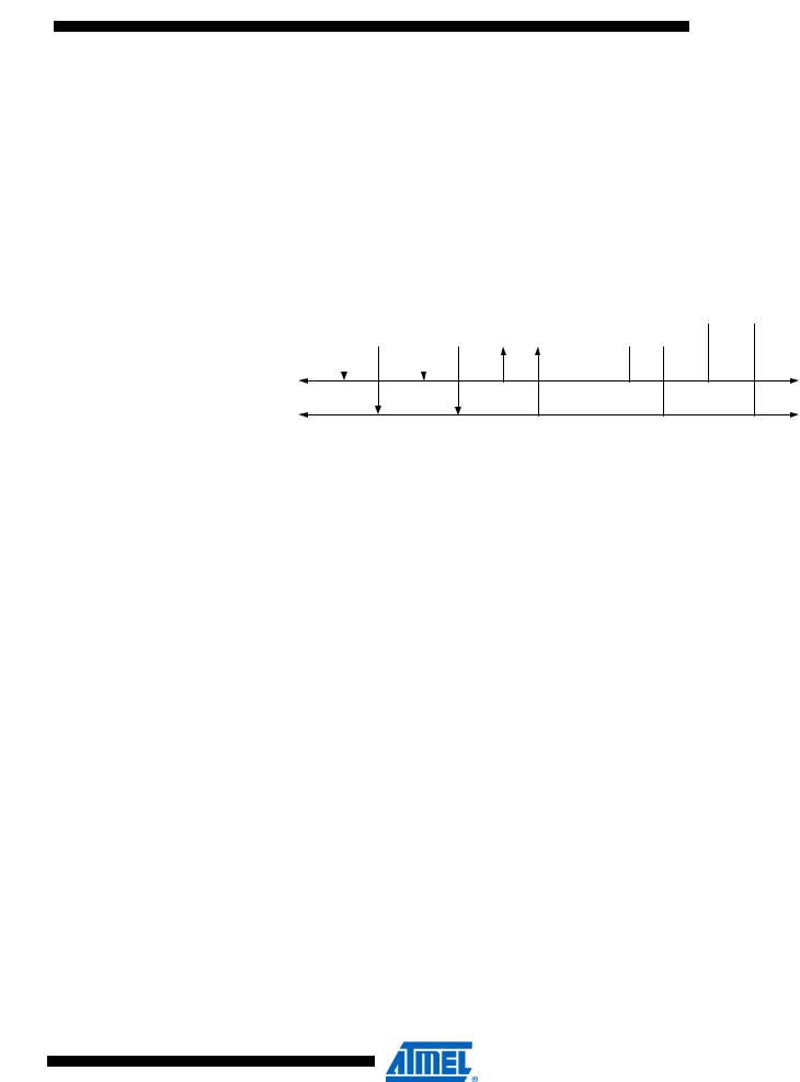
Note that data is transmitted both from master to slave and vice versa. The master must instruct the slave what location it wants to read, requiring the use of the MT mode. Subsequently, data must be read from the slave, implying the use of the MR mode. Thus, the transfer direction must be changed. The master must keep control of the bus during all these steps, and the steps should be carried out as an atomical operation. If this principle is violated in a multimaster system, another master can alter the data pointer in the EEPROM between steps 2 and 3, and the master will read the wrong data location. Such a change in transfer direction is accomplished by transmitting a REPEATED START between the transmission of the address byte and reception of the data. After a REPEATED START, the master keeps ownership of the bus. The following figure shows the flow in this transfer.
Figure 104. Combining Several TWI Modes to Access a Serial EEPROM
|
|
|
Master Transmitter |
|
|
|
Master Receiver |
|
S |
SLA+W |
A |
ADDRESS |
A Rs |
SLA+R |
A |
DATA |
A P |
S = START |
|
|
Rs = REPEATED START |
|
|
P = STOP |
||
|
Transmitted from master to slave |
Transmitted from slave to master |
|
|||||
224
2467X–AVR–06/11
Multi-master
Systems and
Arbitration
ATmega128
If multiple masters are connected to the same bus, transmissions may be initiated simultaneously by one or more of them. The TWI standard ensures that such situations are handled in such a way that one of the masters will be allowed to proceed with the transfer, and that no data will be lost in the process. An example of an arbitration situation is depicted below, where two masters are trying to transmit data to a slave receiver.
Figure 105. An Arbitration Example
|
|
|
|
|
|
|
|
VCC |
|
|
|
|
|
|
|
|
|
|
|
|
|
|
|
|
|
|
|
|
|
|
|
|
|
|
|
|
|
|
|
|
|
|
|
|
|
|
|
|
|
|
Device 1 |
|
Device 2 |
|
Device 3 |
........ |
|
|
|
|
|
|
|
|
|
||
|
|
Device n |
|
|
R1 |
|
R2 |
|
||||||||
|
MASTER |
|
|
MASTER |
|
SLAVE |
|
|
|
|
||||||
TRANSMITTER |
|
TRANSMITTER |
|
RECEIVER |
|
|
|
|
|
|
|
|
|
|
||
|
|
|
|
|
|
|
|
|
|
|
|
|
|
|
|
|
|
|
|
|
|
|
|
|
|
|
|
|
|
|
|
|
|
|
|
|
|
|
|
|
|
|
|
|
|
|
|
|
|
|
SDA
SCL
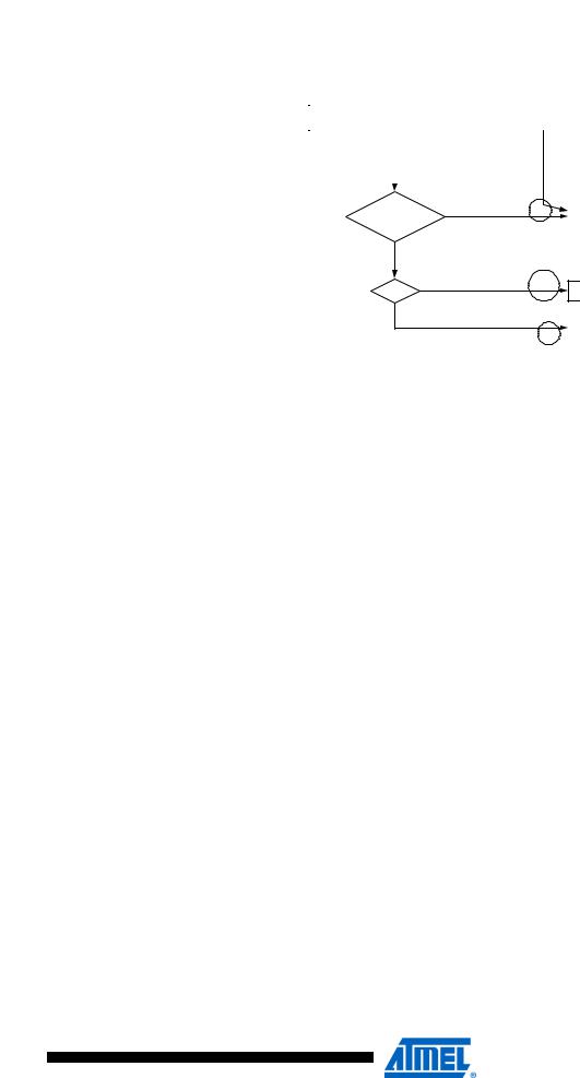
Several different scenarios may arise during arbitration, as described below:
•Two or more masters are performing identical communication with the same slave. In this case, neither the slave nor any of the masters will know about the bus contention.
•Two or more masters are accessing the same slave with different data or direction bit. In this case, arbitration will occur, either in the READ/WRITE bit or in the data bits. The masters trying to output a one on SDA while another master outputs a zero will lose the arbitration. Losing masters will switch to not addressed slave mode or wait until the bus is free and transmit a new START condition, depending on application software action.
•Two or more masters are accessing different slaves. In this case, arbitration will occur in the SLA bits. Masters trying to output a one on SDA while another master outputs a zero will lose the arbitration. Masters losing arbitration in SLA will switch to slave mode to check if they are being addressed by the winning master. If addressed, they will switch to SR or ST mode, depending on the value of the READ/WRITE bit. If they are not being addressed, they will switch to not addressed slave mode or wait until the bus is free and transmit a new START condition, depending on application software action.
This is summarized in Figure 106. Possible status values are given in circles.
225
2467X–AVR–06/11
 ATmega128
Figure 106. Possible Status Codes Caused by Arbitration
START |
|
SLA |
Data |
STOP |
|
|
|
|
|
|
|
Arbitration lost in SLA |
Arbitration lost in Data |
|
|
|
|
|
|
Own |
No |
|
Address / General Call |
||
|
||
received |
|
Yes
Write
Direction
Read
38 |
|
|
TWI bus will be released and not addressed slave mode will be entered |
||
|
A START condition will be transmitted when the bus becomes free |
|
|
|
|
68/78 Data byte will be received and NOT ACK will be returned Data byte will be received and ACK will be returned
|
|
|
|
Last data byte will be transmitted and NOT ACK should be received |
|
B0 |
Data byte will be transmitted and ACK should be received |
|
|
|
|
226
2467X–AVR–06/11