


 ATmega128
Asynchronous Timer |
The Asynchronous Timer clock allows the Asynchronous Timer/Counter to be clocked directly |
Clock – clkASY |
from an external 32kHz clock crystal. The dedicated clock domain allows using this Timer/Coun- |
|
ter as a real-time counter even when the device is in sleep mode. |
ADC Clock – clkADC |
The ADC is provided with a dedicated clock domain. This allows halting the CPU and I/O clocks |
|
in order to reduce noise generated by digital circuitry. This gives more accurate ADC conversion |
|
results. |
XTAL Divide Control The XTAL Divide Control Register is used to divide the Source clock frequency by a number in Register – XDIV the range 2 - 129. This feature can be used to decrease power consumption when the require-
ment for processing power is low.
Bit |
7 |
6 |
5 |
4 |
3 |
2 |
1 |
0 |
|
|
XDIVEN |
XDIV6 |
XDIV5 |
XDIV4 |
XDIV3 |
XDIV2 |
XDIV1 |
XDIV0 |
XDIV |
|
|
|
|
|
|
|
|
|
|
Read/Write |
R/W |
R/W |
R/W |
R/W |
R/W |
R/W |
R/W |
R/W |
|
Initial Value |
0 |
0 |
0 |
0 |
0 |
0 |
0 |
0 |
|
• Bit 7 – XDIVEN: XTAL Divide Enable
When the XDIVEN bit is written one, the clock frequency of the CPU and all peripherals (clkI/O,
clkADC, clkCPU, clkFLASH) is divided by the factor defined by the setting of XDIV6 - XDIV0. This bit can be written run-time to vary the clock frequency as suitable to the application.
• Bits 6..0 – XDIV6..XDIV0: XTAL Divide Select Bits 6 - 0
These bits define the division factor that applies when the XDIVEN bit is set (one). If the value of these bits is denoted d, the following formula defines the resulting CPU and peripherals clock frequency fCLK:
fCLK |
= Source---------------------clock------------ |
|
129 – d |
Clock Sources
The value of these bits can only be changed when XDIVEN is zero. When XDIVEN is written to one, the value written simultaneously into XDIV6..XDIV0 is taken as the division factor. When XDIVEN is written to zero, the value written simultaneously into XDIV6..XDIV0 is rejected. As the divider divides the master clock input to the MCU, the speed of all peripherals is reduced when a division factor is used.
When the system clock is divided, Timer/Counter0 can be used with Asynchronous clock only. The frequency of the asynchronous clock must be lower than 1/4th of the frequency of the scaled down Source clock. Otherwise, interrupts may be lost, and accessing the Timer/Counter0 registers may fail.
The device has the following clock source options, selectable by Flash fuse bits as shown below. The clock from the selected source is input to the AVR clock generator, and routed to the appropriate modules.
Table 6. Device Clocking Options Select
Device Clocking Option |
CKSEL3..0(1) |
External Crystal/Ceramic Resonator |
1111 - 1010 |
|
|
External Low-frequency Crystal |
1001 |
|
|
External RC Oscillator |
1000 - 0101 |
|
|
Calibrated Internal RC Oscillator |
0100 - 0001 |
|
|
External Clock |
0000 |
|
|
36
2467X–AVR–06/11

Default Clock
Source
ATmega128
Note: 1. For all fuses “1” means unprogrammed while “0” means programmed.
The various choices for each clocking option is given in the following sections. When the CPU wakes up from Power-down or Power-save, the selected clock source is used to time the startup, ensuring stable Oscillator operation before instruction execution starts. When the CPU starts from reset, there is as an additional delay allowing the power to reach a stable level before commencing normal operation. The Watchdog Oscillator is used for timing this real-time part of the start-up time. The number of WDT Oscillator cycles used for each time-out is shown in Table 7. The frequency of the Watchdog Oscillator is voltage dependent as shown in the “Typical Characteristics” on page 333.
Table 7. Number of Watchdog Oscillator Cycles
Typical Time-out (VCC = 5.0V) |
Typical Time-Out (VCC = 3.0V) |
Number of Cycles |
|
4.1ms |
4.3ms |
4K |
(4,096) |
|
|
|
|
65ms |
69ms |
64K |
(65,536) |
|
|
|
|
The device is shipped with CKSEL = “0001” and SUT = “10”. The default clock source setting is therefore the Internal RC Oscillator with longest startup time. This default setting ensures that all users can make their desired clock source setting using an In-System or Parallel Programmer.
37
2467X–AVR–06/11
 ATmega128
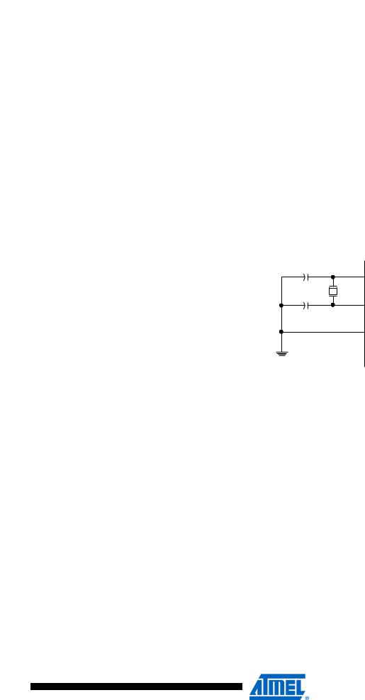
Crystal Oscillator XTAL1 and XTAL2 are input and output, respectively, of an inverting amplifier which can be configured for use as an On-chip Oscillator, as shown in Figure 19. Either a quartz crystal or a ceramic resonator may be used. The CKOPT fuse selects between two different Oscillator Amplifier modes. When CKOPT is programmed, the Oscillator output will oscillate will a full rail- to-rail swing on the output. This mode is suitable when operating in a very noisy environment or when the output from XTAL2 drives a second clock buffer. This mode has a wide frequency range. When CKOPT is unprogrammed, the Oscillator has a smaller output swing. This reduces power consumption considerably. This mode has a limited frequency range and it can not be used to drive other clock buffers.
For resonators, the maximum frequency is 8MHz with CKOPT unprogrammed and 16MHz with CKOPT programmed. C1 and C2 should always be equal for both crystals and resonators. The optimal value of the capacitors depends on the crystal or resonator in use, the amount of stray capacitance, and the electromagnetic noise of the environment. Some initial guidelines for choosing capacitors for use with crystals are given in Table 8. For ceramic resonators, the capacitor values given by the manufacturer should be used.
Figure 19. Crystal Oscillator Connections
C2
XTAL2
C1
XTAL1
GND
The Oscillator can operate in three different modes, each optimized for a specific frequency range. The operating mode is selected by the fuses CKSEL3..1 as shown in Table 8.
Table 8. Crystal Oscillator Operating Modes
|
|
Frequency Range |
Recommended Range for Capacitors |
CKOPT |
CKSEL3..1 |
(MHz) |
C1 and C2 for Use with Crystals |
|
|
|
|
1 |
101(1) |
0.4 - 0.9 |
– |
1 |
110 |
0.9 - 3.0 |
12 - 22pF |
|
|
|
|
1 |
111 |
3.0 - 8.0 |
12 - 22pF |
|
|
|
|
0 |
101, 110, 111 |
1.0 - |
12 - 22pF |
|
|
|
|
Note: 1. |
This option should not be used with crystals, only with ceramic resonators. |
||
The CKSEL0 fuse together with the SUT1..0 fuses select the start-up times as shown in Table 9.
38
2467X–AVR–06/11

 ATmega128
Low-frequency
Crystal Oscillator
Table 9. Start-up Times for the Crystal Oscillator Clock Selection
|
|
Start-up Time from |
Additional Delay |
|
|
|
Power-down and |
from Reset |
|
CKSEL0 |
SUT1..0 |
Power-save |
(VCC = 5.0V) |
Recommended Usage |
0 |
00 |
258 CK(1) |
4.1ms |
Ceramic resonator, fast |
|
|
|
rising power |
|
|
|
|
|
|
|
|
|
|
|
0 |
01 |
258 CK(1) |
65ms |
Ceramic resonator, |
|
|
|
slowly rising power |
|
|
|
|
|
|
|
|
|
|
|
0 |
10 |
1K CK(2) |
– |
Ceramic resonator, |
|
|
|
BOD enabled |
|
|
|
|
|
|
|
|
|
|
|
0 |
11 |
1K CK(2) |
4.0ms |
Ceramic resonator, fast |
|
|
|
rising power |
|
|
|
|
|
|
|
|
|
|
|
1 |
00 |
1K CK(2) |
65ms |
Ceramic resonator, |
|
|
|
slowly rising power |
|
|
|
|
|
|
|
|
|
|
|
1 |
01 |
16K CK |
– |
Crystal Oscillator, BOD |
|
|
|
enabled |
|
|
|
|
|
|
|
|
|
|
|
1 |
10 |
16K CK |
4.1ms |
Crystal Oscillator, fast |
|
|
|
rising power |
|
|
|
|
|
|
|
|
|
|
|
1 |
11 |
16K CK |
65ms |
Crystal Oscillator, |
|
|
|
slowly rising power |
|
|
|
|
|
|
|
|
|
|
|
Notes: 1. These options should only be used when not operating close to the maximum frequency of the device, and only if frequency stability at start-up is not important for the application. These options are not suitable for crystals.
2.These options are intended for use with ceramic resonators and will ensure frequency stability at start-up. They can also be used with crystals when not operating close to the maximum frequency of the device, and if frequency stability at start-up is not important for the application.
To use a 32.768kHz watch crystal as the clock source for the device, the Low-frequency Crystal Oscillator must be selected by setting the CKSEL fuses to “1001”. The crystal should be connected as shown in Figure 19. By programming the CKOPT fuse, the user can enable internal capacitors on XTAL1 and XTAL2, thereby removing the need for external capacitors. The internal capacitors have a nominal value of 36pF.
When this Oscillator is selected, start-up times are determined by the SUT fuses as shown in Table 10.
Table 10. Start-up Times for the Low-frequency Crystal Oscillator Clock Selection
|
Start-up Time from |
Additional Delay |
|
|
|
Power-down and |
from Reset |
|
|
SUT1..0 |
Power-save |
(VCC = 5.0V) |
Recommended Usage |
|
00 |
1K CK(1) |
4.1ms |
Fast rising power or BOD enabled |
|
01 |
1K CK(1) |
65ms |
Slowly rising power |
|
10 |
32K CK |
65ms |
Stable frequency at start-up |
|
|
|
|
|
|
11 |
|
Reserved |
|
|
|
|
|
|
|
Note: 1. |
These options should only be used if frequency stability at start-up is not important for the |
|||
|
application. |
|
|
|
39
2467X–AVR–06/11

External RC
Oscillator
ATmega128
For timing insensitive applications, the External RC configuration shown in Figure 20 can be used. The frequency is roughly estimated by the equation f = 1/(3RC). C should be at least 22pF. By programming the CKOPT fuse, the user can enable an internal 36pF capacitor between XTAL1 and GND, thereby removing the need for an external capacitor. For more information on Oscillator operation and details on how to choose R and C, refer to the External RC Oscillator application note.
Figure 20. External RC Configuration
|
VCC |
|
|
|
R |
|
NC |
|
XTAL2 |
|
||||
|
|
|||
|
|
|
|
|
|
|
|
|
|
XTAL1
C
 GND
GND
The Oscillator can operate in four different modes, each optimized for a specific frequency range. The operating mode is selected by the fuses CKSEL3..0 as shown in Table 11.
Table 11. External RC Oscillator Operating Modes
CKSEL3..0 |
Frequency Range (MHz) |
|
|
0101 |
0.1 - 0.9 |
|
|
0110 |
0.9 - 3.0 |
|
|
0111 |
3.0 - 8.0 |
|
|
1000 |
8.0 - 12.0 |
|
|
When this Oscillator is selected, start-up times are determined by the SUT fuses as shown in Table 12.
Table 12. Start-Up Times for the External RC Oscillator Clock Selection
|
Start-up Time from |
Additional Delay |
|
|
|
Power-down and |
from Reset |
|
|
SUT1..0 |
Power-save |
(VCC = 5.0V) |
Recommended Usage |
|
00 |
18 CK |
– |
BOD enabled |
|
|
|
|
|
|
01 |
18 CK |
4.1ms |
Fast rising power |
|
|
|
|
|
|
10 |
18 CK |
65ms |
Slowly rising power |
|
|
|
|
|
|
11 |
6 CK(1) |
4.1ms |
Fast rising power or BOD enabled |
|
Note: 1. |
This option should not be used when operating close to the maximum frequency of the device. |
|||
40
2467X–AVR–06/11
 ATmega128
Calibrated Internal
RC Oscillator
The Calibrated Internal RC Oscillator provides a fixed 1.0, 2.0, 4.0, or 8.0MHz clock. All frequencies are nominal values at 5V and 25°C. This clock may be selected as the system clock by programming the CKSEL fuses as shown in Table 13. If selected, it will operate with no external components. The CKOPT fuse should always be unprogrammed when using this clock option. During Reset, hardware loads the calibration byte for the 1MHz oscillator into the OSCCAL Register and thereby automatically calibrates the RC Oscillator. At 5V, 25°C and 1.0MHz Oscillator frequency selected, this calibration gives a frequency within ±3% of the nominal frequency. Using calibration methods as described in application notes available at www.atmel.com/avr it is possible to achieve ±1% accuracy at any given VCC and Temperature. When this Oscillator is used as the chip clock, the Watchdog Oscillator will still be used for the Watchdog Timer and for the Reset Time-out. For more information on the pre-programmed calibration value, see the section “Calibration Byte” on page 289.
Table 13. Internal Calibrated RC Oscillator Operating Modes
CKSEL3..0 |
Nominal Frequency (MHz) |
|
|
0001(1) |
1.0 |
0010 |
2.0 |
|
|
0011 |
4.0 |
|
|
0100 |
8.0 |
|
|
Note: 1. The device is shipped with this option selected.
When this Oscillator is selected, start-up times are determined by the SUT fuses as shown in Table 14. XTAL1 and XTAL2 should be left unconnected (NC).
Table 14. Start-up Times for the Internal Calibrated RC Oscillator Clock Selection
|
Start-up Time from Power- |
Additional Delay from |
|
SUT1..0 |
down and Power-save |
Reset (VCC = 5.0V) |
Recommended Usage |
00 |
6 CK |
– |
BOD enabled |
|
|
|
|
01 |
6 CK |
4.1ms |
Fast rising power |
|
|
|
|
10(1) |
6 CK |
65ms |
Slowly rising power |
11 |
|
Reserved |
|
|
|
|
|
Notes: 1. The device is shipped with this option selected.
Oscillator Calibration
Register – OSCCAL
Bit |
7 |
6 |
5 |
4 |
3 |
2 |
1 |
0 |
|
|
CAL7 |
CAL6 |
CAL5 |
CAL4 |
CAL3 |
CAL2 |
CAL1 |
CAL0 |
OSCCAL |
|
|
|
|
|
|
|
|
|
|
Read/Write |
R/W |
R/W |
R/W |
R/W |
R/W |
R/W |
R/W |
R/W |
|
Initial Value |
|
|
Device Specific Calibration Value |
|
|
|
|||
Note: OSCCAL Register is not available in ATmega103 compatibility mode.
• Bits 7..0 – CAL7..0: Oscillator Calibration Value
Writing the calibration byte to this address will trim the Internal Oscillator to remove process variations from the Oscillator frequency. During Reset, the 1MHz calibration value which is located in the signature row high byte (address 0x00) is automatically loaded into the OSCCAL Register. If the internal RC is used at other frequencies, the calibration values must be loaded manually. This can be done by first reading the signature row by a programmer, and then store the calibration values in the Flash or EEPROM. Then the value can be read by software and loaded into the OSCCAL Register. When OSCCAL is zero, the lowest available frequency is chosen. Writing non-zero values to this register will increase the frequency of the Internal Oscillator. Writing $FF
41
2467X–AVR–06/11