

- •Features
- •Overview
- •Block Diagram
- •Pin Descriptions
- •Port A (PA7..PA0)
- •Port B (PB7..PB0)
- •Port C (PC7..PC0)
- •Port D (PD7..PD0)
- •Port E (PE7..PE0)
- •Port F (PF7..PF0)
- •Port G (PG4..PG0)
- •RESET
- •XTAL1
- •XTAL2
- •AVCC
- •AREF
- •Resources
- •Data Retention
- •Capacitive touch sensing
- •AVR CPU Core
- •Introduction
- •Status Register
- •Stack Pointer
- •I/O Memory
- •Overview
- •Timing
- •Using all Locations of External Memory Smaller than 64 Kbyte
- •Clock Systems and their Distribution
- •CPU Clock – clkCPU
- •I/O Clock – clkI/O
- •Flash Clock – clkFLASH
- •ADC Clock – clkADC
- •Clock Sources
- •Crystal Oscillator
- •External Clock
- •Idle Mode
- •Power-down Mode
- •Power-save Mode
- •Standby Mode
- •Analog Comparator
- •Brown-out Detector
- •Watchdog Timer
- •Port Pins
- •Resetting the AVR
- •Reset Sources
- •Power-on Reset
- •External Reset
- •Watchdog Reset
- •Watchdog Timer
- •Timed Sequences for Changing the Configuration of the Watchdog Timer
- •Safety Level 0
- •Safety Level 1
- •Safety Level 2
- •Interrupts
- •I/O Ports
- •Introduction
- •Configuring the Pin
- •Reading the Pin Value
- •Unconnected pins
- •Alternate Port Functions
- •Register Description for I/O Ports
- •8-bit Timer/Counter0 with PWM and Asynchronous Operation
- •Overview
- •Registers
- •Definitions
- •Counter Unit
- •Normal Mode
- •Fast PWM Mode
- •8-bit Timer/Counter Register Description
- •Overview
- •Registers
- •Definitions
- •Compatibility
- •Counter Unit
- •Input Capture Unit
- •Noise Canceler
- •Force Output Compare
- •Normal Mode
- •Fast PWM Mode
- •16-bit Timer/Counter Register Description
- •Internal Clock Source
- •Prescaler Reset
- •External Clock Source
- •8-bit Timer/Counter2 with PWM
- •Overview
- •Registers
- •Definitions
- •Counter Unit
- •Normal Mode
- •Fast PWM Mode
- •8-bit Timer/Counter Register Description
- •Output Compare Modulator (OCM1C2)
- •Overview
- •Description
- •Timing Example
- •Slave Mode
- •Master Mode
- •Data Modes
- •USART
- •Dual USART
- •Overview
- •AVR USART vs. AVR UART – Compatibility
- •Clock Generation
- •External Clock
- •Frame Formats
- •Parity Bit Calculation
- •Parity Generator
- •Receiver Error Flags
- •Parity Checker
- •Disabling the Receiver
- •Using MPCM
- •Features
- •TWI Terminology
- •Transferring Bits
- •Address Packet Format
- •Data Packet Format
- •Overview of the TWI Module
- •Scl and SDA Pins
- •Bus Interface Unit
- •Address Match Unit
- •Control Unit
- •Using the TWI
- •Master Receiver Mode
- •Slave Receiver Mode
- •Miscellaneous States
- •Analog Comparator
- •Analog to Digital Converter
- •Features
- •Operation
- •Changing Channel or Reference Selection
- •ADC Input Channels
- •Analog Input Circuitry
- •Features
- •Overview
- •TAP Controller
- •PRIVATE0; $8
- •PRIVATE1; $9
- •PRIVATE2; $A
- •PRIVATE3; $B
- •Bibliography
- •Features
- •System Overview
- •Data Registers
- •Bypass Register
- •Reset Register
- •EXTEST; $0
- •IDCODE; $1
- •AVR_RESET; $C
- •BYPASS; $F
- •Scanning the ADC
- •ATmega128 Boundary-scan Order
- •Application Section
- •Programming Time for Flash when Using SPM
- •Simple Assembly Code Example for a Boot Loader
- •Fuse Bits
- •Latching of Fuses
- •Signature Bytes
- •Calibration Byte
- •Signal Names
- •Chip Erase
- •Reading the Flash
- •Reading the EEPROM
- •Data Polling Flash
- •Data Polling EEPROM
- •AVR_RESET ($C)
- •PROG_ENABLE ($4)
- •Data Registers
- •Reset Register
- •Programming Enable Register
- •Programming Command Register
- •Virtual Flash Page Read Register
- •Performing Chip Erase
- •Reading the Flash
- •Reading the EEPROM
- •Electrical Characteristics
- •Absolute Maximum Ratings*
- •DC Characteristics
- •Speed Grades
- •External Clock Drive Waveforms
- •External Clock Drive
- •Two-wire Serial Interface Characteristics
- •ADC Characteristics
- •External Data Memory Timing
- •Idle Supply Current
- •Pin Pull-up
- •Pin Driver Strength
- •Register Summary
- •Instruction Set Summary
- •Ordering Information
- •Packaging Information
- •Errata
- •ATmega128 Rev. F to M
 ATmega128
Overview of the
TWI Module
Scl and SDA Pins
Bit Rate Generator
Unit
Bus Interface Unit
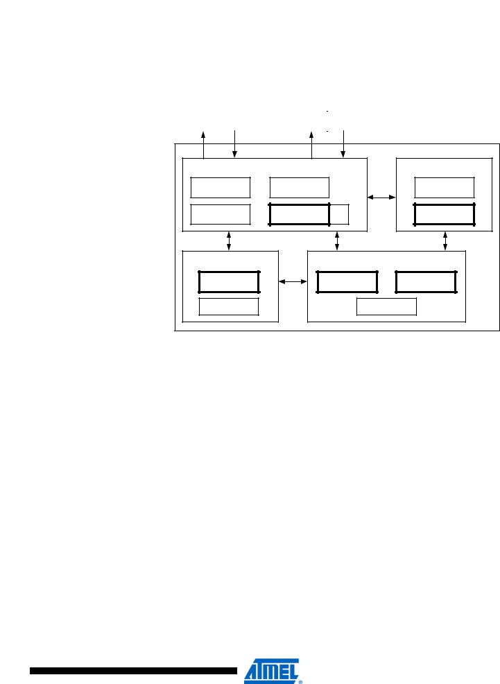
The TWI module is comprised of several submodules, as shown in Figure 94. All registers drawn in a thick line are accessible through the AVR data bus.
Figure 94. Overview of the TWI Module
SCL |
|
SDA |
||
|
|
|
|
|
Slew-rate |
Spike |
|
Slew-rate |
Spike |
Control |
Filter |
|
Control |
Filter |
|
|
|
|
|
Bus Interface Unit |
|
Bit Rate Generator |
||
START / STOP |
Spike Suppression |
|
Prescaler |
|
Control |
|
|
||
|
|
|
|
|
Arbitration detection |
Address/Data Shift |
Ack |
Bit Rate Register |
|
Register (TWDR) |
(TWBR) |
|
||
|
|
|
||
Address Match Unit |
|
Control Unit |
Unit |
|
Address Register |
|
Status Register |
Control Register |
|
(TWAR) |
|
(TWSR) |
(TWCR) |
TWI |
Address Comparator |
|
State Machine and |
||
|
|
|||
|
|
Status control |
|
|
|
|
|
|
|
These pins interface the AVR TWI with the rest of the MCU system. The output drivers contain a slew-rate limiter in order to conform to the TWI specification. The input stages contain a spike suppression unit removing spikes shorter than 50ns. Note that the internal pull-ups in the AVR pads can be enabled by setting the PORT bits corresponding to the SCL and SDA pins, as explained in the I/O Port section. The internal pull-ups can in some systems eliminate the need for external ones.
This unit controls the period of SCL when operating in a Master mode. The SCL period is controlled by settings in the TWI Bit Rate Register (TWBR) and the Prescaler bits in the TWI Status Register (TWSR). Slave operation does not depend on Bit Rate or Prescaler settings, but the CPU clock frequency in the slave must be at least 16 times higher than the SCL frequency. Note that slaves may prolong the SCL low period, thereby reducing the average TWI bus clock period. The SCL frequency is generated according to the following equation:
CPU Clock frequency SCL frequency = ----------------------------------------------------------
16 + 2(TWBR) 4TWPS
• TWBR = Value of the TWI Bit Rate Register
• TWPS = Value of the prescaler bits in the TWI Status Register
Note: Pull-up resistor values should be selected according to the SCL frequency and the capacitive bus line load. See Table 133 on page 322 for value of pull-up resistor.
This unit contains the Data and Address Shift Register (TWDR), a START/STOP Controller and Arbitration detection hardware. The TWDR contains the address or data bytes to be transmitted, or the address or data bytes received. In addition to the 8-bit TWDR, the Bus Interface Unit also contains a register containing the (N)ACK bit to be transmitted or received. This (N)ACK Register is not directly accessible by the application software. However, when receiving, it can be set
203
2467X–AVR–06/11

 ATmega128
|
or cleared by manipulating the TWI Control Register (TWCR). When in Transmitter mode, the |
|
value of the received (N)ACK bit can be determined by the value in the TWSR. |
|
The START/STOP Controller is responsible for generation and detection of START, REPEATED |
|
START, and STOP conditions. The START/STOP controller is able to detect START and STOP |
|
conditions even when the AVR MCU is in one of the sleep modes, enabling the MCU to wake up |
|
if addressed by a master. |
|
If the TWI has initiated a transmission as master, the Arbitration Detection hardware continu- |
|
ously monitors the transmission trying to determine if arbitration is in process. If the TWI has lost |
|
an arbitration, the Control Unit is informed. Correct action can then be taken and appropriate |
|
status codes generated. |
Address Match Unit |
The Address Match unit checks if received address bytes match the 7-bit address in the TWI |
|
Address Register (TWAR). If the TWI General Call Recognition Enable (TWGCE) bit in the |
|
TWAR is written to one, all incoming address bits will also be compared against the General Call |
|
address. Upon an address match, the Control Unit is informed, allowing correct action to be |
|
taken. The TWI may or may not acknowledge its address, depending on settings in the TWCR. |
|
The Address Match unit is able to compare addresses even when the AVR MCU is in sleep |
|
mode, enabling the MCU to wake up if addressed by a master. If another interrupt (e.g., INT0) |
|
occurs during TWI Power-down address match and wakes up the CPU, the TWI aborts opera- |
|
tion and return to it’s idle state. If this cause any problems, ensure that TWI Address Match is the |
|
only enabled interrupt when entering Power-down. |
Control Unit |
The Control unit monitors the TWI bus and generates responses corresponding to settings in the |
|
TWI Control Register (TWCR). When an event requiring the attention of the application occurs |
|
on the TWI bus, the TWI Interrupt Flag (TWINT) is asserted. In the next clock cycle, the TWI Sta- |
|
tus Register (TWSR) is updated with a status code identifying the event. The TWSR only |
|
contains relevant status information when the TWI Interrupt Flag is asserted. At all other times, |
|
the TWSR contains a special status code indicating that no relevant status information is avail- |
|
able. As long as the TWINT flag is set, the SCL line is held low. This allows the application |
|
software to complete its tasks before allowing the TWI transmission to continue. |
The TWINT flag is set in the following situations:
•After the TWI has transmitted a START/REPEATED START condition
•After the TWI has transmitted SLA+R/W
•After the TWI has transmitted an address byte
•After the TWI has lost arbitration
•After the TWI has been addressed by own slave address or general call
•After the TWI has received a data byte
•After a STOP or REPEATED START has been received while still addressed as a slave
•When a bus error has occurred due to an illegal START or STOP condition
204
2467X–AVR–06/11

 ATmega128
TWI Register
Description
TWI Bit Rate Register
– TWBR
Bit |
7 |
6 |
5 |
4 |
3 |
2 |
1 |
0 |
|
|
TWBR7 |
TWBR6 |
TWBR5 |
TWBR4 |
TWBR3 |
TWBR2 |
TWBR1 |
TWBR0 |
TWBR |
|
|
|
|
|
|
|
|
|
|
Read/Write |
R/W |
R/W |
R/W |
R/W |
R/W |
R/W |
R/W |
R/W |
|
Initial Value |
0 |
0 |
0 |
0 |
0 |
0 |
0 |
0 |
|
• Bits 7..0 – TWI Bit Rate Register
TWI Control Register –
TWCR
TWBR selects the division factor for the bit rate generator. The bit rate generator is a frequency divider which generates the SCL clock frequency in the Master modes. See “Bit Rate Generator Unit” on page 203 for calculating bit rates.
Bit |
7 |
6 |
5 |
4 |
3 |
2 |
1 |
0 |
|
|
TWINT |
TWEA |
TWSTA |
TWSTO |
TWWC |
TWEN |
– |
TWIE |
TWCR |
|
|
|
|
|
|
|
|
|
|
Read/Write |
R/W |
R/W |
R/W |
R/W |
R |
R/W |
R |
R/W |
|
Initial Value |
0 |
0 |
0 |
0 |
0 |
0 |
0 |
0 |
|
The TWCR is used to control the operation of the TWI. It is used to enable the TWI, to initiate a master access by applying a START condition to the bus, to generate a receiver acknowledge, to generate a stop condition, and to control halting of the bus while the data to be written to the bus are written to the TWDR. It also indicates a write collision if data is attempted written to TWDR while the register is inaccessible.
• Bit 7 – TWINT: TWI Interrupt Flag
This bit is set by hardware when the TWI has finished its current job and expects application software response. If the I-bit in SREG and TWIE in TWCR are set, the MCU will jump to the TWI interrupt vector. While the TWINT flag is set, the SCL low period is stretched.
The TWINT flag must be cleared by software by writing a logic one to it. Note that this flag is not automatically cleared by hardware when executing the interrupt routine. Also note that clearing this flag starts the operation of the TWI, so all accesses to the TWI Address Register (TWAR), TWI Status Register (TWSR), and TWI Data Register (TWDR) must be complete before clearing this flag.
• Bit 6 – TWEA: TWI Enable Acknowledge Bit
The TWEA bit controls the generation of the acknowledge pulse. If the TWEA bit is written to one, the ACK pulse is generated on the TWI bus if the following conditions are met:
1.The device’s own slave address has been received.
2.A general call has been received, while the TWGCE bit in the TWAR is set.
3.A data byte has been received in Master Receiver or Slave Receiver mode.
By writing the TWEA bit to zero, the device can be virtually disconnected from the Two-wire Serial Bus temporarily. Address recognition can then be resumed by writing the TWEA bit to one again.
• Bit 5 – TWSTA: TWI START Condition Bit
The application writes the TWSTA bit to one when it desires to become a master on the Twowire Serial Bus. The TWI hardware checks if the bus is available, and generates a START condition on the bus if it is free. However, if the bus is not free, the TWI waits until a STOP condition is detected, and then generates a new START condition to claim the bus Master status. TWSTA must be cleared by software when the START condition has been transmitted.
205
2467X–AVR–06/11

 ATmega128
TWI Status Register –
TWSR
• Bit 4 – TWSTO: TWI STOP Condition Bit
Writing the TWSTO bit to one in Master mode will generate a STOP condition on the Two-wire Serial Bus. When the STOP condition is executed on the bus, the TWSTO bit is cleared automatically. In slave mode, setting the TWSTO bit can be used to recover from an error condition. This will not generate a STOP condition, but the TWI returns to a well-defined unaddressed Slave mode and releases the SCL and SDA lines to a high impedance state.
• Bit 3 – TWWC: TWI Write Collision Flag
The TWWC bit is set when attempting to write to the TWI Data Register – TWDR when TWINT is low. This flag is cleared by writing the TWDR Register when TWINT is high.
• Bit 2 – TWEN: TWI Enable Bit
The TWEN bit enables TWI operation and activates the TWI interface. When TWEN is written to one, the TWI takes control over the I/O pins connected to the SCL and SDA pins, enabling the slew-rate limiters and spike filters. If this bit is written to zero, the TWI is switched off and all TWI transmissions are terminated, regardless of any ongoing operation.
• Bit 1 – Res: Reserved Bit
This bit is a reserved bit and will always read as zero.
• Bit 0 – TWIE: TWI Interrupt Enable
When this bit is written to one, and the I-bit in SREG is set, the TWI interrupt request will be activated for as long as the TWINT flag is high.
Bit |
7 |
6 |
5 |
4 |
3 |
2 |
1 |
0 |
|
|
TWS7 |
TWS6 |
TWS5 |
TWS4 |
TWS3 |
– |
TWPS1 |
TWPS0 |
TWSR |
|
|
|
|
|
|
|
|
|
|
Read/Write |
R |
R |
R |
R |
R |
R |
R/W |
R/W |
|
Initial Value |
1 |
1 |
1 |
1 |
1 |
0 |
0 |
0 |
|
• Bits 7..3 – TWS: TWI Status
These 5 bits reflect the status of the TWI logic and the Two-wire Serial Bus. The different status codes are described later in this section. Note that the value read from TWSR contains both the 5-bit status value and the 2-bit prescaler value. The application designer should mask the prescaler bits to zero when checking the Status bits. This makes status checking independent of prescaler setting. This approach is used in this datasheet, unless otherwise noted.
• Bit 2 – Res: Reserved Bit
This bit is reserved and will always read as zero.
• Bits 1..0 – TWPS: TWI Prescaler Bits
These bits can be read and written, and control the bit rate prescaler.
Table 87. TWI Bit Rate Prescaler
TWPS1 |
TWPS0 |
Prescaler Value |
|
|
|
0 |
0 |
1 |
|
|
|
0 |
1 |
4 |
|
|
|
1 |
0 |
16 |
|
|
|
1 |
1 |
64 |
|
|
|
To calculate bit rates, see “Bit Rate Generator Unit” on page 203. The value of TWPS1..0 is used in the equation.
206
2467X–AVR–06/11