


 ATmega128
Stack Pointer
RAM Page Z Select
Register – RAMPZ
Instruction
Execution Timing
The Stack is mainly used for storing temporary data, for storing local variables and for storing return addresses after interrupts and subroutine calls. The Stack Pointer Register always points to the top of the Stack. Note that the Stack is implemented as growing from higher memory locations to lower memory locations. This implies that a Stack PUSH command decreases the Stack Pointer.
The Stack Pointer points to the data SRAM stack area where the Subroutine and Interrupt Stacks are located. This Stack space in the data SRAM must be defined by the program before any subroutine calls are executed or interrupts are enabled. The Stack Pointer must be set to point above $60. The Stack Pointer is decremented by one when data is pushed onto the Stack with the PUSH instruction, and it is decremented by two when the return address is pushed onto the Stack with subroutine call or interrupt. The Stack Pointer is incremented by one when data is popped from the Stack with the POP instruction, and it is incremented by two when data is popped from the Stack with return from subroutine RET or return from interrupt RETI.
The AVR Stack Pointer is implemented as two 8-bit registers in the I/O space. The number of bits actually used is implementation dependent. Note that the data space in some implementations of the AVR architecture is so small that only SPL is needed. In this case, the SPH Register will not be present.
Bit |
15 |
14 |
13 |
12 |
11 |
|
10 |
9 |
8 |
|
|
SP15 |
SP14 |
SP13 |
SP12 |
SP11 |
SP10 |
SP9 |
SP8 |
SPH |
|
|
|
|
|
|
|
|
|
|
|
|
|
SP7 |
SP6 |
SP5 |
SP4 |
SP3 |
SP2 |
SP1 |
SP0 |
SPL |
|
|
|
|
|
|
|
|
|
|
|
|
|
7 |
6 |
5 |
4 |
3 |
|
2 |
1 |
0 |
|
Read/Write |
R/W |
R/W |
R/W |
R/W |
R/W |
R/W |
R/W |
R/W |
|
|
|
R/W |
R/W |
R/W |
R/W |
R/W |
R/W |
R/W |
R/W |
|
|
Initial Value |
0 |
0 |
0 |
0 |
0 |
|
0 |
0 |
0 |
|
|
0 |
0 |
0 |
0 |
0 |
|
0 |
0 |
0 |
|
Bit |
7 |
6 |
5 |
4 |
3 |
|
2 |
1 |
0 |
|
|
|
|
|
|
|
|
|
|
|
|
|
– |
–– |
– |
– |
– |
|
– |
– |
RAMPZ0 |
RAMPZ |
|
|
|
|
|
|
|
|
|
|
|
Read/Write |
R |
R |
R |
R |
R |
R |
R |
R/W |
|
|
Initial Value |
0 |
0 |
0 |
0 |
0 |
|
0 |
0 |
0 |
|
• Bits 7..1 – Res: Reserved Bits
These are reserved bits and will always read as zero. When writing to this address location, write these bits to zero for compatibility with future devices.
• Bit 0 – RAMPZ0: Extended RAM Page Z-pointer
The RAMPZ Register is normally used to select which 64K RAM Page is accessed by the Z- pointer. As the ATmega128 does not support more than 64K of SRAM memory, this register is used only to select which page in the program memory is accessed when the ELPM/SPM instruction is used. The different settings of the RAMPZ0 bit have the following effects:
RAMPZ0 = 0: Program memory address $0000 - $7FFF (lower 64 Kbytes) is accessed by ELPM/SPM
RAMPZ0 = 1: Program memory address $8000 - $FFFF (higher 64 Kbytes) is accessed by ELPM/SPM
Note that LPM is not affected by the RAMPZ setting.
This section describes the general access timing concepts for instruction execution. The AVR CPU is driven by the CPU clock clkCPU, directly generated from the selected clock source for the chip. No internal clock division is used.
13
2467X–AVR–06/11

 ATmega128
Figure 6 shows the parallel instruction fetches and instruction executions enabled by the Harvard architecture and the fast-access Register file concept. This is the basic pipelining concept to obtain up to 1 MIPS per MHz with the corresponding unique results for functions per cost, functions per clocks, and functions per power-unit.
Figure 6. The Parallel Instruction Fetches and Instruction Executions
T1 |
T2 |
T3 |
T4 |
clkCPU
1st Instruction Fetch
1st Instruction Execute 2nd Instruction Fetch 2nd Instruction Execute 3rd Instruction Fetch 3rd Instruction Execute 4th Instruction Fetch
Figure 7 shows the internal timing concept for the Register file. In a single clock cycle an ALU operation using two register operands is executed, and the result is stored back to the destination register.
Figure 7. Single Cycle ALU Operation
T1 |
T2 |
T3 |
T4 |
clkCPU Total Execution Time
Register Operands Fetch
ALU Operation Execute
Result Write Back
Reset and
Interrupt Handling
The AVR provides several different interrupt sources. These interrupts and the separate reset vector each have a separate program vector in the program memory space. All interrupts are assigned individual enable bits which must be written logic one together with the Global Interrupt Enable bit in the Status Register in order to enable the interrupt. Depending on the Program Counter value, interrupts may be automatically disabled when Boot Lock bits BLB02 or BLB12 are programmed. This feature improves software security. See the section “Memory Programming” on page 286 for details.
The lowest addresses in the program memory space are by default defined as the Reset and Interrupt vectors. The complete list of vectors is shown in “Interrupts” on page 59. The list also determines the priority levels of the different interrupts. The lower the address the higher is the priority level. RESET has the highest priority, and next is INT0 – the External Interrupt Request 0. The interrupt vectors can be moved to the start of the boot Flash section by setting the IVSEL bit in the MCU Control Register (MCUCR). Refer to “Interrupts” on page 59 for more information. The Reset vector can also be moved to the start of the boot Flash section by programming the BOOTRST fuse, see “Boot Loader Support – Read-While-Write Self-Programming” on page 273.
When an interrupt occurs, the Global Interrupt Enable I-bit is cleared and all interrupts are disabled. The user software can write logic one to the I-bit to enable nested interrupts. All enabled interrupts can then interrupt the current interrupt routine. The I-bit is automatically set when a Return from Interrupt instruction – RETI – is executed.
14
2467X–AVR–06/11

 ATmega128
There are basically two types of interrupts. The first type is triggered by an event that sets the interrupt flag. For these interrupts, the Program Counter is vectored to the actual interrupt vector in order to execute the interrupt handling routine, and hardware clears the corresponding interrupt flag. Interrupt flags can also be cleared by writing a logic one to the flag bit position(s) to be cleared. If an interrupt condition occurs while the corresponding interrupt enable bit is cleared, the interrupt flag will be set and remembered until the interrupt is enabled, or the flag is cleared by software. Similarly, if one or more interrupt conditions occur while the global interrupt enable bit is cleared, the corresponding interrupt flag(s) will be set and remembered until the global interrupt enable bit is set, and will then be executed by order of priority.
The second type of interrupts will trigger as long as the interrupt condition is present. These interrupts do not necessarily have interrupt flags. If the interrupt condition disappears before the interrupt is enabled, the interrupt will not be triggered.
When the AVR exits from an interrupt, it will always return to the main program and execute one more instruction before any pending interrupt is served.
Note that the Status Register is not automatically stored when entering an interrupt routine, nor restored when returning from an interrupt routine. This must be handled by software.
When using the CLI instruction to disable interrupts, the interrupts will be immediately disabled. No interrupt will be executed after the CLI instruction, even if it occurs simultaneously with the CLI instruction. The following example shows how this can be used to avoid interrupts during the timed EEPROM write sequence.
Assembly Code Example
in r16, SREG ; store SREG value
cli ; disable interrupts during timed sequence sbi EECR, EEMWE ; start EEPROM write
sbi EECR, EEWE
out SREG, r16 ; restore SREG value (I-bit)
C Code Example
char cSREG;
cSREG = SREG; /* store SREG value */
/* disable interrupts during timed sequence */
__disable_interrupt();
EECR |= (1<<EEMWE); /* start EEPROM write */
EECR |= (1<<EEWE);
SREG = cSREG; /* restore SREG value (I-bit) */
15
2467X–AVR–06/11

 ATmega128
When using the SEI instruction to enable interrupts, the instruction following SEI will be executed before any pending interrupts, as shown in this example.
Assembly Code Example
sei ; set global interrupt enable
sleep; enter sleep, waiting for interrupt
;note: will enter sleep before any pending
;interrupt(s)
C Code Example
__enable_interrupt(); /* set global interrupt enable */
__sleep(); /* enter sleep, waiting for interrupt */
/* note: will enter sleep before any pending interrupt(s) */
Interrupt Response The interrupt execution response for all the enabled AVR interrupts is four clock cycles mini- Time mum. After four clock cycles, the program vector address for the actual interrupt handling routine is executed. During this 4-clock cycle period, the Program Counter is pushed onto the Stack.
The vector is normally a jump to the interrupt routine, and this jump takes three clock cycles. If an interrupt occurs during execution of a multi-cycle instruction, this instruction is completed before the interrupt is served. If an interrupt occurs when the MCU is in Sleep mode, the interrupt execution response time is increased by four clock cycles. This increase comes in addition to the start-up time from the selected sleep mode.
A return from an interrupt handling routine takes four clock cycles. During these 4-clock cycles, the Program Counter (two bytes) is popped back from the Stack, the Stack Pointer is incremented by two, and the I-bit in SREG is set.
16
2467X–AVR–06/11

 ATmega128
AVR
ATmega128
Memories
In-System
Reprogrammable
Flash Program
Memory
This section describes the different memories in the Atmel® AVR® ATmega128. The AVR architecture has two main memory spaces, the Data Memory and the Program Memory space. In addition, the ATmega128 features an EEPROM Memory for data storage. All three memory spaces are linear and regular.
The ATmega128 contains 128Kbytes On-chip In-System Reprogrammable Flash memory for program storage. Since all AVR instructions are 16 or 32 bits wide, the Flash is organized as 64K x 16. For software security, the Flash Program memory space is divided into two sections, Boot Program section and Application Program section.
The Flash memory has an endurance of at least 10,000 write/erase cycles. The ATmega128 Program Counter (PC) is 16 bits wide, thus addressing the 64K program memory locations. The operation of Boot Program section and associated Boot Lock bits for software protection are described in detail in “Boot Loader Support – Read-While-Write Self-Programming” on page 273. “Memory Programming” on page 286 contains a detailed description on Flash programming in SPI, JTAG, or Parallel Programming mode.
Constant tables can be allocated within the entire program memory address space (see the LPM
– Load Program Memory and ELPM – Extended Load Program Memory instruction description).
Timing diagrams for instruction fetch and execution are presented in “Instruction Execution Timing” on page 13.
Figure 8. Program Memory Map
Program Memory
$0000
Application Flash Section
Boot Flash Section
$FFFF
17
2467X–AVR–06/11

SRAM Data
Memory
ATmega128
The Atmel® AVR® ATmega128 supports two different configurations for the SRAM data memory as listed in Table 1.
Table 1. Memory Configurations
Configuration |
Internal SRAM Data Memory |
External SRAM Data Memory |
|
|
|
|
|
Normal mode |
4096 |
up to 64K |
|
|
|
|
|
ATmega103 Compatibility |
4000 |
up to 64K |
|
mode |
|||
|
|
||
|
|
|
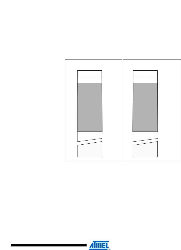
Figure 9 shows how the ATmega128 SRAM Memory is organized.
The ATmega128 is a complex microcontroller with more peripheral units than can be supported within the 64 location reserved in the Opcode for the IN and OUT instructions. For the Extended I/O space from $60 - $FF in SRAM, only the ST/STS/STD and LD/LDS/LDD instructions can be used. The Extended I/O space does not exist when the ATmega128 is in the ATmega103 compatibility mode.
In normal mode, the first 4352 Data Memory locations address both the Register file, the I/O Memory, Extended I/O Memory, and the internal data SRAM. The first 32 locations address the Register file, the next 64 location the standard I/O memory, then 160 locations of Extended I/O memory, and the next 4096 locations address the internal data SRAM.
In ATmega103 compatibility mode, the first 4096 Data Memory locations address both the Register file, the I/O Memory and the internal data SRAM. The first 32 locations address the Register file, the next 64 location the standard I/O memory, and the next 4000 locations address the internal data SRAM.
An optional external data SRAM can be used with the ATmega128. This SRAM will occupy an area in the remaining address locations in the 64K address space. This area starts at the address following the internal SRAM. The Register file, I/O, Extended I/O and Internal SRAM occupies the lowest 4352bytes in normal mode, and the lowest 4096bytes in the ATmega103 compatibility mode (Extended I/O not present), so when using 64Kbyte (65536 bytes) of External Memory, 61184bytes of External Memory are available in normal mode, and 61440 bytes in ATmega103 compatibility mode. See “External Memory Interface” on page 25 for details on how to take advantage of the external memory map.
When the addresses accessing the SRAM memory space exceeds the internal data memory locations, the external data SRAM is accessed using the same instructions as for the internal data memory access. When the internal data memories are accessed, the read and write strobe pins (PG0 and PG1) are inactive during the whole access cycle. External SRAM operation is enabled by setting the SRE bit in the MCUCR Register.
Accessing external SRAM takes one additional clock cycle per byte compared to access of the internal SRAM. This means that the commands LD, ST, LDS, STS, LDD, STD, PUSH, and POP take one additional clock cycle. If the Stack is placed in external SRAM, interrupts, subroutine calls and returns take three clock cycles extra because the two-byte program counter is pushed and popped, and external memory access does not take advantage of the internal pipe-line memory access. When external SRAM interface is used with wait-state, one-byte external access takes two, three, or four additional clock cycles for one, two, and three wait-states respectively. Interrupts, subroutine calls and returns will need five, seven, or nine clock cycles more than specified in the instruction set manual for one, two, and three wait-states.
The five different addressing modes for the data memory cover: Direct, Indirect with Displacement, Indirect, Indirect with Pre-decrement, and Indirect with Post-increment. In the Register file, registers R26 to R31 feature the indirect addressing pointer registers.
The direct addressing reaches the entire data space.
18
2467X–AVR–06/11
 ATmega128
The Indirect with Displacement mode reaches 63 address locations from the base address given by the Y- or Z-register.
When using register indirect addressing modes with automatic pre-decrement and post-incre- ment, the address registers X, Y, and Z are decremented or incremented.
The 32 general purpose working registers, 64 I/O registers, and the 4096bytes of internal data SRAM in the ATmega128 are all accessible through all these addressing modes. The Register file is described in “General Purpose Register File” on page 11.
Figure 9. Data Memory Map
Memory Configuration A |
Memory Configuration B |
||||
|
Data Memory |
|
|
Data Memory |
|
|
|
$0000 - $001F |
|
|
$0000 - $001F |
|
32 Registers |
|
32 Registers |
||
|
64 I/O Registers |
$0020 - $005F |
|
64 I/O Registers |
$0020 - $005F |
|
160 Ext I/O Reg. |
$0060 - $00FF |
|
Internal SRAM |
$0060 |
|
|
$0100 |
|
|
|
|
Internal SRAM |
|
|
(4000 x 8) |
$0FFF |
|
(4096 x 8) |
|
|
|
|
|
|
$10FF |
|
|
$1000 |
|
|
|
|
|
|
|
|
$1100 |
|
|
|
|
External SRAM |
|
|
External SRAM |
|
|
(0 - 64K x 8) |
|
|
(0 - 64K x 8) |
|
$FFFF |
$FFFF |
19
2467X–AVR–06/11

 ATmega128
Data Memory Access This section describes the general access timing concepts for internal memory access. The
Times |
internal data SRAM access is performed in two clkCPU cycles as described in Figure 10. |
|||
|
Figure 10. On-chip Data SRAM Access Cycles |
|
||
|
|
T1 |
T2 |
T3 |
|
clkCPU |
|
|
|
|
Address |
Compute Address |
Address valid |
|
Data 
WR 
Data 
RD 
Read Write
Memory access instruction |
Next instruction |
EEPROM Data
Memory
EEPROM Read/Write
Access
The Atmel® AVR®ATmega128 contains 4Kbytes of data EEPROM memory. It is organized as a separate data space, in which single bytes can be read and written. The EEPROM has an endurance of at least 100,000 write/erase cycles. The access between the EEPROM and the CPU is described in the following, specifying the EEPROM Address Registers, the EEPROM Data Register, and the EEPROM Control Register.
“Memory Programming” on page 286 contains a detailed description on EEPROM programming in SPI, JTAG, or Parallel Programming mode
The EEPROM access registers are accessible in the I/O space.
The write access time for the EEPROM is given in Table 2. A self-timing function, however, lets the user software detect when the next byte can be written. If the user code contains instructions that write the EEPROM, some precautions must be taken. In heavily filtered power supplies, VCC is likely to rise or fall slowly on Power-up/down. This causes the device for some period of time to run at a voltage lower than specified as minimum for the clock frequency used. See “Preventing EEPROM Corruption” on page 24. for details on how to avoid problems in these situations.
In order to prevent unintentional EEPROM writes, a specific write procedure must be followed. Refer to the description of the EEPROM Control Register for details on this.
When the EEPROM is read, the CPU is halted for four clock cycles before the next instruction is executed. When the EEPROM is written, the CPU is halted for two clock cycles before the next instruction is executed.
EEPROM Address
Register – EEARH and
EEARL
Bit |
15 |
14 |
13 |
12 |
11 |
10 |
9 |
8 |
|
|
– |
– |
– |
– |
EEAR11 |
EEAR10 |
EEAR9 |
EEAR8 |
EEARH |
|
|
|
|
|
|
|
|
|
|
|
EEAR7 |
EEAR6 |
EEAR5 |
EEAR4 |
EEAR3 |
EEAR2 |
EEAR1 |
EEAR0 |
EEARL |
|
|
|
|
|
|
|
|
|
|
|
7 |
6 |
5 |
4 |
3 |
2 |
1 |
0 |
|
Read/Write |
R |
R |
R |
R |
R/W |
R/W |
R/W |
R/W |
|
|
R/W |
R/W |
R/W |
R/W |
R/W |
R/W |
R/W |
R/W |
|
Initial Value |
0 |
0 |
0 |
0 |
X |
X |
X |
X |
|
|
X |
X |
X |
X |
X |
X |
X |
X |
|
• Bits 15..12 – Res: Reserved Bits
These are reserved bits and will always read as zero. When writing to this address location, write these bits to zero for compatibility with future devices.
20
2467X–AVR–06/11
 ATmega128
EEPROM Data
Register – EEDR
EEPROM Control
Register – EECR
• Bits 11..0 – EEAR11..0: EEPROM Address
The EEPROM Address Registers – EEARH and EEARL – specify the EEPROM address in the 4 Kbytes EEPROM space. The EEPROM data bytes are addressed linearly between 0 and 4096. The initial value of EEAR is undefined. A proper value must be written before the EEPROM may be accessed.
Bit |
7 |
6 |
5 |
4 |
3 |
2 |
1 |
0 |
|
|
MSB |
|
|
|
|
|
|
LSB |
EEDR |
|
|
|
|
|
|
|
|
|
|
Read/Write |
R/W |
R/W |
R/W |
R/W |
R/W |
R/W |
R/W |
R/W |
|
Initial Value |
0 |
0 |
0 |
0 |
0 |
0 |
0 |
0 |
|
• Bits 7..0 – EEDR7.0: EEPROM Data
For the EEPROM write operation, the EEDR Register contains the data to be written to the EEPROM in the address given by the EEAR Register. For the EEPROM read operation, the EEDR contains the data read out from the EEPROM at the address given by EEAR.
Bit |
7 |
6 |
5 |
4 |
3 |
2 |
1 |
0 |
|
|
– |
– |
– |
– |
EERIE |
EEMWE |
EEWE |
EERE |
EECR |
|
|
|
|
|
|
|
|
|
|
Read/Write |
R |
R |
R |
R |
R/W |
R/W |
R/W |
R/W |
|
Initial Value |
0 |
0 |
0 |
0 |
0 |
0 |
X |
0 |
|
• Bits 7..4 – Res: Reserved Bits
These bits are reserved bits in the ATmega128 and will always read as zero.
• Bit 3 – EERIE: EEPROM Ready Interrupt Enable
Writing EERIE to one enables the EEPROM Ready Interrupt if the I-bit in SREG is set. Writing EERIE to zero disables the interrupt. The EEPROM Ready interrupt generates a constant interrupt when EEWE is cleared.
• Bit 2 – EEMWE: EEPROM Master Write Enable
The EEMWE bit determines whether setting EEWE to one causes the EEPROM to be written. When EEMWE is written to one, writing EEWE to one within four clock cycles will write data to the EEPROM at the selected address. If EEMWE is zero, writing EEWE to one will have no effect. When EEMWE has been written to one by software, hardware clears the bit to zero after four clock cycles. See the description of the EEWE bit for an EEPROM write procedure.
• Bit 1 – EEWE: EEPROM Write Enable
The EEPROM Write Enable Signal EEWE is the write strobe to the EEPROM. When address and data are correctly set up, the EEWE bit must be set to write the value into the EEPROM. The EEMWE bit must be set when the logical one is written to EEWE, otherwise no EEPROM write takes place. The following procedure should be followed when writing the EEPROM (the order of steps 3 and 4 is not essential):
1.Wait until EEWE becomes zero.
2.Wait until SPMEN in SPMCSR becomes zero.
3.Write new EEPROM address to EEAR (optional).
4.Write new EEPROM data to EEDR (optional).
5.Write a logical one to the EEMWE bit while writing a zero to EEWE in EECR.
6.Within four clock cycles after setting EEMWE, write a logical one to EEWE.
21
2467X–AVR–06/11

 ATmega128
The EEPROM can not be programmed during a CPU write to the Flash memory. The software must check that the Flash programming is completed before initiating a new EEPROM write. Step 2 is only relevant if the software contains a boot loader allowing the CPU to program the Flash. If the Flash is never being updated by the CPU, step 2 can be omitted. See “Boot Loader Support – Read-W hile-Write Self-Programming” on page 273 for details about boot programming.
Caution: An interrupt between step 5 and step 6 will make the write cycle fail, since the EEPROM Master Write Enable will time-out. If an interrupt routine accessing the EEPROM is interrupting another EEPROM access, the EEAR or EEDR Register will be modified, causing the interrupted EEPROM access to fail. It is recommended to have the global interrupt flag cleared during the four last steps to avoid these problems.
When the write access time has elapsed, the EEWE bit is cleared by hardware. The user software can poll this bit and wait for a zero before writing the next byte. When EEWE has been set, the CPU is halted for two cycles before the next instruction is executed.
• Bit 0 – EERE: EEPROM Read Enable
The EEPROM Read Enable Signal EERE is the read strobe to the EEPROM. When the correct address is set up in the EEAR Register, the EERE bit must be written to a logic one to trigger the EEPROM read. The EEPROM read access takes one instruction, and the requested data is available immediately. When the EEPROM is read, the CPU is halted for four cycles before the next instruction is executed.
The user should poll the EEWE bit before starting the read operation. If a write operation is in progress, it is neither possible to read the EEPROM, nor to change the EEAR Register.
The calibrated Oscillator is used to time the EEPROM accesses. Table 2 lists the typical programming time for EEPROM access from the CPU.
Table 2. EEPROM Programming Time
|
Number of Calibrated RC |
|
Symbol |
Oscillator Cycles(1) |
Typ Programming Time |
EEPROM Write (from CPU) |
8448 |
8.5ms |
|
|
|
Note: 1. Uses 1MHz clock, independent of CKSEL-fuse settings.
22
2467X–AVR–06/11

 ATmega128
The following code examples show one assembly and one C function for writing to the EEPROM. The examples assume that interrupts are controlled (for example, by disabling interrupts globally) so that no interrupts will occur during execution of these functions. The examples also assume that no flash boot loader is present in the software. If such code is present, the EEPROM write function must also wait for any ongoing SPM command to finish.
Assembly Code Example
EEPROM_write:
; Wait for completion of previous write sbic EECR,EEWE
rjmp EEPROM_write
; Set up address (r18:r17) in address register out EEARH, r18
out EEARL, r17
; Write data (r16) to data register out EEDR,r16
; Write logical one to EEMWE sbi EECR,EEMWE
; Start eeprom write by setting EEWE sbi EECR,EEWE
ret
C Code Example
void EEPROM_write(unsigned int uiAddress, unsigned char ucData)
{
/* Wait for completion of previous write */ while(EECR & (1<<EEWE))
;
/* Set up address and data registers */ EEAR = uiAddress;
EEDR = ucData;
/* Write logical one to EEMWE */
EECR |= (1<<EEMWE);
/* Start eeprom write by setting EEWE */
EECR |= (1<<EEWE);
}
23
2467X–AVR–06/11

 ATmega128
The next code examples show assembly and C functions for reading the EEPROM. The examples assume that interrupts are controlled so that no interrupts will occur during execution of these functions.
Assembly Code Example
EEPROM_read:
; Wait for completion of previous write sbic EECR,EEWE
rjmp EEPROM_read
; Set up address (r18:r17) in address register out EEARH, r18
out EEARL, r17
; Start eeprom read by writing EERE sbi EECR,EERE
; Read data from data register in r16,EEDR
ret
C Code Example
unsigned char EEPROM_read(unsigned int uiAddress)
{
/* Wait for completion of previous write */ while(EECR & (1<<EEWE))
;
/* Set up address register */ EEAR = uiAddress;
/* Start eeprom read by writing EERE */
EECR |= (1<<EERE);
/* Return data from data register */ return EEDR;
}
EEPROM Write During When entering Power-down sleep mode while an EEPROM write operation is active, the Power-down Sleep EEPROM write operation will continue, and will complete before the write access time has Mode passed. However, when the write operation is completed, the Oscillator continues running, and as a consequence, the device does not enter Power-down entirely. It is therefore recommended
to verify that the EEPROM write operation is completed before entering Power-down.
Preventing EEPROM During periods of low VCC, the EEPROM data can be corrupted because the supply voltage is Corruption too low for the CPU and the EEPROM to operate properly. These issues are the same as for
board level systems using EEPROM, and the same design solutions should be applied.
An EEPROM data corruption can be caused by two situations when the voltage is too low. First, a regular write sequence to the EEPROM requires a minimum voltage to operate correctly. Secondly, the CPU itself can execute instructions incorrectly, if the supply voltage is too low.
EEPROM data corruption can easily be avoided by following this design recommendation:
Keep the AVR RESET active (low) during periods of insufficient power supply voltage. This can be done by enabling the internal Brown-out Detector (BOD). If a reset occurs while a write oper-
24
2467X–AVR–06/11