

- •Features
- •Overview
- •Block Diagram
- •Pin Descriptions
- •Port A (PA7..PA0)
- •Port B (PB7..PB0)
- •Port C (PC7..PC0)
- •Port D (PD7..PD0)
- •Port E (PE7..PE0)
- •Port F (PF7..PF0)
- •Port G (PG4..PG0)
- •RESET
- •XTAL1
- •XTAL2
- •AVCC
- •AREF
- •Resources
- •Data Retention
- •Capacitive touch sensing
- •AVR CPU Core
- •Introduction
- •Status Register
- •Stack Pointer
- •I/O Memory
- •Overview
- •Timing
- •Using all Locations of External Memory Smaller than 64 Kbyte
- •Clock Systems and their Distribution
- •CPU Clock – clkCPU
- •I/O Clock – clkI/O
- •Flash Clock – clkFLASH
- •ADC Clock – clkADC
- •Clock Sources
- •Crystal Oscillator
- •External Clock
- •Idle Mode
- •Power-down Mode
- •Power-save Mode
- •Standby Mode
- •Analog Comparator
- •Brown-out Detector
- •Watchdog Timer
- •Port Pins
- •Resetting the AVR
- •Reset Sources
- •Power-on Reset
- •External Reset
- •Watchdog Reset
- •Watchdog Timer
- •Timed Sequences for Changing the Configuration of the Watchdog Timer
- •Safety Level 0
- •Safety Level 1
- •Safety Level 2
- •Interrupts
- •I/O Ports
- •Introduction
- •Configuring the Pin
- •Reading the Pin Value
- •Unconnected pins
- •Alternate Port Functions
- •Register Description for I/O Ports
- •8-bit Timer/Counter0 with PWM and Asynchronous Operation
- •Overview
- •Registers
- •Definitions
- •Counter Unit
- •Normal Mode
- •Fast PWM Mode
- •8-bit Timer/Counter Register Description
- •Overview
- •Registers
- •Definitions
- •Compatibility
- •Counter Unit
- •Input Capture Unit
- •Noise Canceler
- •Force Output Compare
- •Normal Mode
- •Fast PWM Mode
- •16-bit Timer/Counter Register Description
- •Internal Clock Source
- •Prescaler Reset
- •External Clock Source
- •8-bit Timer/Counter2 with PWM
- •Overview
- •Registers
- •Definitions
- •Counter Unit
- •Normal Mode
- •Fast PWM Mode
- •8-bit Timer/Counter Register Description
- •Output Compare Modulator (OCM1C2)
- •Overview
- •Description
- •Timing Example
- •Slave Mode
- •Master Mode
- •Data Modes
- •USART
- •Dual USART
- •Overview
- •AVR USART vs. AVR UART – Compatibility
- •Clock Generation
- •External Clock
- •Frame Formats
- •Parity Bit Calculation
- •Parity Generator
- •Receiver Error Flags
- •Parity Checker
- •Disabling the Receiver
- •Using MPCM
- •Features
- •TWI Terminology
- •Transferring Bits
- •Address Packet Format
- •Data Packet Format
- •Overview of the TWI Module
- •Scl and SDA Pins
- •Bus Interface Unit
- •Address Match Unit
- •Control Unit
- •Using the TWI
- •Master Receiver Mode
- •Slave Receiver Mode
- •Miscellaneous States
- •Analog Comparator
- •Analog to Digital Converter
- •Features
- •Operation
- •Changing Channel or Reference Selection
- •ADC Input Channels
- •Analog Input Circuitry
- •Features
- •Overview
- •TAP Controller
- •PRIVATE0; $8
- •PRIVATE1; $9
- •PRIVATE2; $A
- •PRIVATE3; $B
- •Bibliography
- •Features
- •System Overview
- •Data Registers
- •Bypass Register
- •Reset Register
- •EXTEST; $0
- •IDCODE; $1
- •AVR_RESET; $C
- •BYPASS; $F
- •Scanning the ADC
- •ATmega128 Boundary-scan Order
- •Application Section
- •Programming Time for Flash when Using SPM
- •Simple Assembly Code Example for a Boot Loader
- •Fuse Bits
- •Latching of Fuses
- •Signature Bytes
- •Calibration Byte
- •Signal Names
- •Chip Erase
- •Reading the Flash
- •Reading the EEPROM
- •Data Polling Flash
- •Data Polling EEPROM
- •AVR_RESET ($C)
- •PROG_ENABLE ($4)
- •Data Registers
- •Reset Register
- •Programming Enable Register
- •Programming Command Register
- •Virtual Flash Page Read Register
- •Performing Chip Erase
- •Reading the Flash
- •Reading the EEPROM
- •Electrical Characteristics
- •Absolute Maximum Ratings*
- •DC Characteristics
- •Speed Grades
- •External Clock Drive Waveforms
- •External Clock Drive
- •Two-wire Serial Interface Characteristics
- •ADC Characteristics
- •External Data Memory Timing
- •Idle Supply Current
- •Pin Pull-up
- •Pin Driver Strength
- •Register Summary
- •Instruction Set Summary
- •Ordering Information
- •Packaging Information
- •Errata
- •ATmega128 Rev. F to M

 ATmega128
Boot Loader
Support – Read-
While-Write
Self-
Programming
The Boot Loader Support provides a real Read-While-Write Self-Programming mechanism for downloading and uploading program code by the MCU itself. This feature allows flexible application software updates controlled by the MCU using a Flash-resident Boot Loader program. The Boot Loader program can use any available data interface and associated protocol to read code and write (program) that code into the Flash memory, or read the code from the program memory. The program code within the Boot Loader section has the capability to write into the entire Flash, including the Boot Loader memory. The Boot Loader can thus even modify itself, and it can also erase itself from the code if the feature is not needed anymore. The size of the Boot Loader memory is configurable with fuses and the Boot Loader has two separate sets of Boot Lock bits which can be set independently. This gives the user a unique flexibility to select different levels of protection.
Boot Loader
Features
•Read-While-Write Self-Programming
•Flexible Boot Memory Size
•High Security (Separate Boot Lock Bits for a Flexible Protection)
•Separate Fuse to Select Reset Vector
•Optimized Page(1) Size
•Code Efficient Algorithm
•Efficient Read-Modify-Write Support
Note: 1. A page is a section in the flash consisting of several bytes (see Table 123 on page 291) used during programming. The page organization does not affect normal operation.
Application and
Boot Loader Flash
Sections
Application Section
The Flash memory is organized in two main sections, the Application section and the Boot Loader section (see Figure 133). The size of the different sections is configured by the BOOTSZ fuses as shown in Table on page 284 and Figure 133. These two sections can have different level of protection since they have different sets of Lock bits.
The application section is the section of the Flash that is used for storing the application code. The protection level for the application section can be selected by the application Boot Lock bits (Boot Lock bits 0), see Table on page 275. The application section can never store any Boot Loader code since the SPM instruction is disabled when executed from the application section.
Boot Loader Section – While the application section is used for storing the application code, the The Boot Loader soft- BLS ware must be located in the BLS since the SPM instruction can initiate a programming when executing from the BLS only. The SPM instruction can access the entire Flash, including the BLS itself. The protection level for the Boot Loader section can be selected by the Boot Loader
Lock bits (Boot Lock bits 1), see Table 109 on page 276.
Read-While-Write
and No Read-
While-Write Flash
Sections
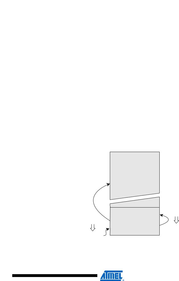
Whether the CPU supports Read-While-Write or if the CPU is halted during a Boot Loader software update is dependent on which address that is being programmed. In addition to the two sections that are configurable by the BOOTSZ fuses as described above, the Flash is also divided into two fixed sections, the Read-While-Write (RWW) section and the No Read-While- Write (NRWW) section. The limit between the RWWand NRWW sections is given in Table Note: on page 284 and Figure 133 on page 275. The main difference between the two sections is:
•When erasing or writing a page located inside the RWW section, the NRWW section can be read during the operation.
•When erasing or writing a page located inside the NRWW section, the CPU is halted during the entire operation.
Note that the user software can never read any code that is located inside the RWW section during a Boot Loader software operation. The syntax “Read-While-Write section” refers to which
273
2467X–AVR–06/11
 ATmega128
section that is being programmed (erased or written), not which section that actually is being read during a Boot Loader software update.
Read-While-Write If a Boot Loader software update is programming a page inside the RWW section, it is possible Section – RWW to read code from the Flash, but only code that is located in the NRWW section. During an ongoing programming, the software must ensure that the RWW section never is being read. If the user software is trying to read code that is located inside the RWW section (i.e., by a call/jmp/lpm or an interrupt) during programming, the software might end up in an unknown state. To avoid this, the interrupts should either be disabled or moved to the Boot Loader Section. The Boot Loader section is always located in the NRWW section. The RWW Section Busy bit (RWWSB) in the Store Program Memory Control and Status Register (SPMCSR) will be read as logical one as long as the RWW section is blocked for reading. After a programming is completed, the RWWSB must be cleared by software before reading code located in the RWW section. See “Store Program Memory Control and Status Register – SPMCSR” on page 277. for
details on how to clear RWWSB.
No Read-While-Write The code located in the NRWW section can be read when the Boot Loader software is updating Section – NRWW a page in the RWW section. When the Boot Loader code updates the NRWW section, the CPU
is halted during the entire page erase or page write operation.
Table 107. Read-While-Write Features
Which Section does the Z- |
Which Section can be |
|
Read-While- |
pointer Address During the |
Read During |
Is the CPU |
Write |
Programming? |
Programming? |
Halted? |
Supported? |
|
|
|
|
RWW section |
NRWW section |
No |
Yes |
|
|
|
|
NRWW section |
None |
Yes |
No |
|
|
|
|
Figure 132. Read-While-Write vs. No Read-While-Write
Read-While-Write
(RWW) Section
|
Z-pointer |
|
Addresses NRWW |
Z-pointer |
Section |
|
|
Addresses RWW |
No Read-While-Write |
Section |
(NRWW) Section |
|
CPU is Halted |
Code Located in |
During the Operation |
|
|
NRWW Section |
|
Can be Read During |
|
the Operation |
|
274
2467X–AVR–06/11
 ATmega128
Boot Loader Lock
Bits
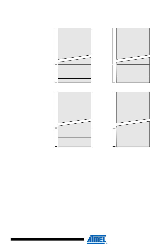
Figure 133. Memory Sections(1)
No Read-While-Write Section Read-While-Write Section No Read-While-Write Section Read-While-Write Section
Program Memory
BOOTSZ = '11'
Application Flash Section
Application Flash Section
Boot Loader Flash Section
Program Memory
BOOTSZ = '01'
Application Flash Section
Application Flash Section
Boot Loader Flash Section
$0000
|
Read-While-Write Section |
End Application |
Write-WhileSection |
End RWW |
|
Start NRWW |
|
Flashend |
- |
Read |
|
Start Boot Loader |
|
|
No |
$0000 |
|
|
Read-While-Write Section |
End Application |
SectionWrite |
End RWW |
|
Start NRWW |
|
Flashend |
- |
-ReadWhile |
|
Start Boot Loader |
|
|
No |
Program Memory
BOOTSZ = '10'
$0000
Application Flash Section
End RWW
Start NRWW
Application Flash Section
End Application
Start Boot Loader
Boot Loader Flash Section
Flashend
Program Memory
BOOTSZ = '00'
$0000
Application flash Section
End RWW, End Application
Start NRWW, Start Boot Loader
Boot Loader Flash Section
Flashend
Note: 1. The parameters in the figure above are given in Table on page 284.
If no Boot Loader capability is needed, the entire Flash is available for application code. The Boot Loader has two separate sets of Boot Lock bits which can be set independently. This gives the user a unique flexibility to select different levels of protection.
The user can select:
•To protect the entire Flash from a software update by the MCU
•To protect only the Boot Loader Flash section from a software update by the MCU
•To protect only the Application Flash section from a software update by the MCU
•Allow software update in the entire Flash
See Table 108 and Table 109 for further details. The Boot Lock bits can be set in software and in Serial or Parallel Programming mode, but they can be cleared by a chip erase command only. The general Write Lock (Lock bit mode 2) does not control the programming of the Flash memory by SPM instruction. Similarly, the general Read/Write Lock (Lock bit mode 3) does not control reading nor writing by LPM/SPM, if it is attempted.
275
2467X–AVR–06/11

 ATmega128
Entering the Boot
Loader Program
Table 108. Boot Lock Bit0 Protection Modes (Application Section)(1)
BLB0 mode |
BLB02 |
BLB01 |
Protection |
|
|
|
|
|
|
1 |
1 |
1 |
No restrictions for SPM or LPM accessing the Application |
|
section. |
||||
|
|
|
||
|
|
|
|
|
2 |
1 |
0 |
SPM is not allowed to write to the Application section. |
|
|
|
|
|
|
|
|
|
SPM is not allowed to write to the Application section, and |
|
|
|
|
LPM executing from the Boot Loader section is not |
|
3 |
0 |
0 |
allowed to read from the Application section. If interrupt |
|
|
|
|
vectors are placed in the Boot Loader section, interrupts |
|
|
|
|
are disabled while executing from the Application section. |
|
|
|
|
|
|
|
|
|
LPM executing from the Boot Loader section is not |
|
4 |
0 |
1 |
allowed to read from the Application section. If interrupt |
|
vectors are placed in the Boot Loader section, interrupts |
||||
|
|
|
||
|
|
|
are disabled while executing from the Application section. |
|
|
|
|
|
|
Note: 1. “1” means unprogrammed, “0” means programmed |
||||
Table 109. Boot Lock Bit1 Protection Modes (Boot Loader Section)(1)
|
|
|
BLB1 |
|
BLB1 mode |
BLB12 |
1 |
Protection |
|
|
|
|
|
|
1 |
|
1 |
1 |
No restrictions for SPM or LPM accessing the Boot Loader |
|
section. |
|||
|
|
|
|
|
|
|
|
|
|
2 |
|
1 |
0 |
SPM is not allowed to write to the Boot Loader section. |
|
|
|
|
|
|
|
|
|
SPM is not allowed to write to the Boot Loader section, |
|
|
|
|
and LPM executing from the Application section is not |
3 |
|
0 |
0 |
allowed to read from the Boot Loader section. If interrupt |
|
|
|
|
vectors are placed in the Application section, interrupts are |
|
|
|
|
disabled while executing from the Boot Loader section. |
|
|
|
|
|
|
|
|
|
LPM executing from the Application section is not allowed |
4 |
|
0 |
1 |
to read from the Boot Loader section. If interrupt vectors |
|
are placed in the Application section, interrupts are |
|||
|
|
|
|
|
|
|
|
|
disabled while executing from the Boot Loader section. |
|
|
|
|
|
Note: |
1. “1” means unprogrammed, “0´means programmed |
|||
Entering the Boot Loader takes place by a jump or call from the application program. This may be initiated by a trigger such as a command received via USART, or SPI interface. Alternatively, the Boot Reset Fuse can be programmed so that the Reset Vector Reset is pointing to the Boot Flash start address after a reset. In this case, the Boot Loader is started after a reset. After the application code is loaded, the program can start executing the application code. Note that the fuses cannot be changed by the MCU itself. This means that once the Boot Reset Fuse is programmed, the Reset Vector will always point to the Boot Loader Reset and the fuse can only be changed through the serial or parallel programming interface.
Table 110. Boot Reset Fuse(1)
BOOTRST |
Reset Address |
|
|
1 |
Reset Vector = Application Reset (address $0000) |
|
|
0 |
Reset Vector = Boot Loader Reset (see Table 112 on page 284) |
|
|
Note: 1. “1” means unprogrammed, “0´means programmed
276
2467X–AVR–06/11

 ATmega128
Store Program |
The Store Program Memory Control and Status Register contains the control bits needed to con- |
|||||||||
Memory Control and |
trol the Boot Loader operations. |
|
|
|
|
|
|
|||
Status Register – |
Bit |
7 |
6 |
5 |
4 |
3 |
2 |
1 |
0 |
|
SPMCSR |
|
|||||||||
|
|
|
|
|
|
|
|
|
|
|
|
SPMIE |
RWWSB |
– |
RWWSRE |
BLBSET |
PGWRT |
PGERS |
SPMEN |
SPMCSR |
|
|
|
|||||||||
|
|
|
|
|
|
|
|
|
|
|
|
Read/Write |
R/W |
R |
R |
R/W |
R/W |
R/W |
R/W |
R/W |
|
|
Initial Value |
0 |
0 |
0 |
0 |
0 |
0 |
0 |
0 |
|
• Bit 7 – SPMIE: SPM Interrupt Enable
When the SPMIE bit is written to one, and the I-bit in the Status Register is set (one), the SPM ready interrupt will be enabled. The SPM ready Interrupt will be executed as long as the SPMEN bit in the SPMCSR Register is cleared.
• Bit 6 – RWWSB: Read-While-Write Section Busy
When a Self-Programming (page erase or page write) operation to the RWW section is initiated, the RWWSB will be set (one) by hardware. When the RWWSB bit is set, the RWW section cannot be accessed. The RWWSB bit will be cleared if the RWWSRE bit is written to one after a self-programming operation is completed. Alternatively the RWWSB bit will automatically be cleared if a page load operation is initiated.
• Bit 5 – Res: Reserved Bit
This bit is a reserved bit in the ATmega128 and always read as zero.
• Bit 4 – RWWSRE: Read-While-Write Section Read Enable
When Programming (page erase or page write) to the RWW section, the RWW section is blocked for reading (the RWWSB will be set by hardware). To re-enable the RWW section, the user software must wait until the programming is completed (SPMEN will be cleared). Then, if the RWWSRE bit is written to one at the same time as SPMEN, the next SPM instruction within four clock cycles re-enables the RWW section. The RWW section cannot be re-enabled while the Flash is busy with a page erase or a page write (SPMEN is set). If the RWWSRE bit is written while the Flash is being loaded, the Flash load operation will abort and the data loaded will be lost.
• Bit 3 – BLBSET: Boot Lock Bit Set
If this bit is written to one at the same time as SPMEN, the next SPM instruction within four clock cycles sets Boot Lock bits, according to the data in R0. The data in R1 and the address in the Z- pointer are ignored. The BLBSET bit will automatically be cleared upon completion of the lock bit set, or if no SPM instruction is executed within four clock cycles.
An LPM instruction within three cycles after BLBSET and SPMEN are set in the SPMCSR Register, will read either the Lock bits or the Fuse bits (depending on Z0 in the Z-pointer) into the destination register. See “Reading the Fuse and Lock Bits from Software” on page 281 for details.
• Bit 2 – PGWRT: Page Write
If this bit is written to one at the same time as SPMEN, the next SPM instruction within four clock cycles executes page write, with the data stored in the temporary buffer. The page address is taken from the high part of the Z-pointer. The data in R1 and R0 are ignored. The PGWRT bit will auto-clear upon completion of a page write, or if no SPM instruction is executed within four clock cycles. The CPU is halted during the entire page write operation if the NRWW section is addressed.
• Bit 1 – PGERS: Page Erase
If this bit is written to one at the same time as SPMEN, the next SPM instruction within four clock cycles executes page erase. The page address is taken from the high part of the Z-pointer. The data in R1 and R0 are ignored. The PGERS bit will auto-clear upon completion of a page erase,
277
2467X–AVR–06/11

 ATmega128
Addressing the
Flash During Self-
Programming
or if no SPM instruction is executed within four clock cycles. The CPU is halted during the entire page write operation if the NRWW section is addressed.
• Bit 0 – SPMEN: Store Program Memory Enable
This bit enables the SPM instruction for the next four clock cycles. If written to one together with either RWWSRE, BLBSET, PGWRT’ or PGERS, the following SPM instruction will have a special meaning, see description above. If only SPMEN is written, the following SPM instruction will store the value in R1:R0 in the temporary page buffer addressed by the Z-pointer. The LSB of the Z-pointer is ignored. The SPMEN bit will auto-clear upon completion of an SPM instruction, or if no SPM instruction is executed within four clock cycles. During page erase and page write, the SPMEN bit remains high until the operation is completed.
Writing any other combination than “10001”, “01001”, “00101”, “00011” or “00001” in the lower five bits will have no effect.
The Z-pointer together with RAMPZ are used to address the SPM commands. For details on how to use the RAMPZ, see “RAM Page Z Select Register – RAMPZ” on page 13.
Bit |
15 |
14 |
13 |
12 |
11 |
10 |
9 |
8 |
|
ZH (R31) |
Z15 |
Z14 |
Z13 |
Z12 |
Z11 |
Z10 |
Z9 |
Z8 |
|
|
|
|
|
|
|
|
|
|
|
ZL (R30) |
Z7 |
Z6 |
Z5 |
Z4 |
Z3 |
Z2 |
Z1 |
Z0 |
|
|
|
|
|
|
|
|
|
|
|
|
|
7 |
6 |
5 |
4 |
3 |
2 |
1 |
0 |
Since the Flash is organized in pages (see Table 123 on page 291), the program counter can be treated as having two different sections. One section, consisting of the least significant bits, is addressing the words within a page, while the most significant bits are addressing the pages. This is shown in Figure 134. Note that the page erase and page write operations are addressed independently. Therefore it is of major importance that the Boot Loader software addresses the same page in both the page erase and page write operation. Once a programming operation is initiated, the address is latched and the Z-pointer/RAMPZ can be used for other operations.
The only SPM operation that does not use the Z-pointer/RAMPZ is setting the Boot Loader Lock bits. The content of the Z-pointer/RAMPZ is ignored and will have no effect on the operation. The (E)LPM instruction does also use the Z-pointer/RAMPZ to store the address. Since this instruction addresses the Flash byte by byte, also the LSB (bit Z0) of the Z-pointer is used.
278
2467X–AVR–06/11

 ATmega128
Figure 134. Addressing the Flash During SPM(1)
|
RAMPZ |
|
|
BIT 15 ZPCMSB |
ZPAGEMSB |
1 0 |
|
|
|
|||||||||||
|
|
|
|
|
|
|
|
|
|
|
|
|
|
|
|
|
0 |
Z - REGISTER |
|
|
|
|
|
|
|
|
|
|
|
|
|
|
|
|
|
|
|
|
|
|
|
|
PROGRAM |
|
PCMSB |
PAGEMSB |
|
|
|
|
|
|
||||||||||
|
|
|
|
|
PCPAGE |
|
PCWORD |
|
|
|
|
|
|
|||||||
|
COUNTER |
|
|
|
|
|
|
|
|
|
|
|
||||||||
|
|
|
|
|
|
|
|
|
|
|
|
|
|
|
|
|
|
|
||
|
|
|
|
|
PAGE ADDRESS |
|
|
WORD ADDRESS |
|
|||||||||||
|
|
|
|
|
WITHIN THE FLASH |
|
|
WITHIN A PAGE |
|
|||||||||||
|
PROGRAM MEMORY |
|
|
|
|
|
|
|
PAGE |
PCWORD[PAGEMSB:0]: |
||||||||||
|
|
|
|
|
|
|
|
|
|
|
|
|
|
|
|
|
|
|
|
|
|
|
|
PAGE |
|
|
|
|
|
INSTRUCTION WORD |
00 |
||||||||||
|
|
|
|
|
|
|
|
|
|
|
|
|
|
|
||||||
|
|
|
|
|
|
|
|
|
|
|
|
|
|
|
|
|
|
|
|
01 |
|
|
|
|
|
|
|
|
|
|
|
|
|
|
|
|
|
|
|
|
|
|
|
|
|
|
|
|
|
|
|
|
|
|
|
|
|
|
|
|
|
02 |
|
|
|
|
|
|
|
|
|
|
|
|
|
|
|
|
|
|
|
|
|
|
|
|
|
|
|
|
|
|
|
|
|
|
|
|
|
|
|
|
|
|
|
|
|
|
|
|
|
|
|
|
|
|
|
|
|
|
|
|
|
|
|
|
|
|
|
|
|
|
|
|
|
|
|
|
|
|
|
|
|
|
|
|
|
|
|
|
|
|
|
|
|
|
|
|
|
|
|
|
|
|
|
|
|
|
|
|
|
|
|
|
|
|
|
|
|
|
|
|
|
|
|
|
|
|
|
|
|
|
|
|
|
|
|
|
|
|
|
|
|
|
|
|
|
|
|
|
|
|
|
|
|
|
|
|
|
|
|
|
|
|
|
|
|
|
|
|
|
|
|
|
|
|
|
|
|
|
|
|
|
|
|
|
|
|
|
|
|
|
|
|
|
|
|
|
|
|
|
|
|
|
|
|
|
|
|
|
|
|
|
|
|
|
|
|
|
|
|
|
|
|
|
|
|
|
|
|
|
|
|
|
|
|
|
|
|
|
|
|
|
|
|
|
|
|
|
|
|
|
|
|
|
|
|
|
|
|
|
|
|
|
|
|
|
|
|
|
|
|
|
|
|
|
|
|
|
|
|
|
|
|
|
|
|
|
|
|
|
|
|
|
|
|
PAGEEND
Self-Programming
the Flash
Notes: 1. The different variables used in Figure 134 are listed in Table 114 on page 285. 2. PCPAGE and PCWORD are listed in Table 124 on page 291.
The program memory is updated in a page by page fashion. Before programming a page with the data stored in the temporary page buffer, the page must be erased. The temporary page buffer is filled one word at a time using SPM and the buffer can be filled either before the page erase command or between a page erase and a page write operation:
Alternative 1, fill the buffer before a page erase
•Fill temporary page buffer
•Perform a page erase
•Perform a page write
Alternative 2, fill the buffer after page erase
•Perform a page erase
•Fill temporary page buffer
•Perform a page write
If only a part of the page needs to be changed, the rest of the page must be stored (for example in the temporary page buffer) before the erase, and then be rewritten. When using alternative 1, the Boot Loader provides an effective Read-Modify-Write feature which allows the user software to first read the page, do the necessary changes, and then write back the modified data. If alternative 2 is used, it is not possible to read the old data while loading since the page is already erased. The temporary page buffer can be accessed in a random sequence. It is essential that the page address used in both the page erase and page write operation is addressing the same page. See “Simple Assembly Code Example for a Boot Loader” on page 282 for an assembly code example.
279
2467X–AVR–06/11

 ATmega128
Performing Page |
To execute page erase, set up the address in the Z-pointer and RAMPZ, write “X0000011” to |
Erase by SPM |
SPMCSR and execute SPM within four clock cycles after writing SPMCSR. The data in R1 and |
|
R0 is ignored. The page address must be written to PCPAGE in the Z-register. Other bits in the |
|
Z-pointer must be written zero during this operation. |
|
• Page Erase to the RWW section: The NRWW section can be read during the page erase. |
|
• Page Erase to the NRWW section: The CPU is halted during the operation. |
Filling the Temporary |
To write an instruction word, set up the address in the Z-pointer and data in R1:R0, write |
Buffer (Page Loading) |
“00000001” to SPMCSR and execute SPM within four clock cycles after writing SPMCSR. The |
|
content of PCWORD in the Z-register is used to address the data in the temporary buffer. The |
|
temporary buffer will auto-erase after a page write operation or by writing the RWWSRE bit in |
|
SPMCSR. It is also erased after a System Reset. Note that it is not possible to write more than |
|
one time to each address without erasing the temporary buffer. |
|
Note: If the EEPROM is written in the middle of an SPM Page Load operation, all data loaded will be |
|
lost. |
Performing a Page |
To execute page write, set up the address in the Z-pointer and RAMPZ, write “X0000101” to |
Write |
SPMCSR and execute SPM within four clock cycles after writing SPMCSR. The data in R1 and |
|
R0 is ignored. The page address must be written to PCPAGE. Other bits in the Z-pointer must |
|
be written zero during this operation. |
|
• Page Write to the RWW section: The NRWW section can be read during the page write. |
|
• Page Write to the NRWW section: The CPU is halted during the operation. |
Using the SPM |
If the SPM interrupt is enabled, the SPM interrupt will generate a constant interrupt when the |
Interrupt |
SPMEN bit in SPMCSR is cleared. This means that the interrupt can be used instead of polling |
|
the SPMCSR Register in software. When using the SPM interrupt, the interrupt vectors should |
|
be moved to the BLS section to avoid that an interrupt is accessing the RWW section when it is |
|
blocked for reading. How to move the interrupts is described in “Interrupts” on page 59. |
Consideration While |
Special care must be taken if the user allows the Boot Loader section to be updated by leaving |
Updating BLS |
Boot Lock bit11 unprogrammed. An accidental write to the Boot Loader itself can corrupt the |
|
entire Boot Loader, and further software updates might be impossible. If it is not necessary to |
|
change the Boot Loader software itself, it is recommended to program the Boot Lock bit11 to |
|
protect the Boot Loader software from any internal software changes. |
Prevent Reading the |
During Self-Programming (either page erase or page write), the RWW section is always blocked |
RWW Section During |
for reading. The user software itself must prevent that this section is addressed during the Self- |
Self-Programming |
Programming operation. The RWWSB in the SPMCSR will be set as long as the RWW section is |
|
busy. During Self-Programming the interrupt vector table should be moved to the BLS as |
|
described in “Interrupts” on page 59, or the interrupts must be disabled. Before addressing the |
|
RWW section after the programming is completed, the user software must clear the RWWSB by |
|
writing the RWWSRE. See “Simple Assembly Code Example for a Boot Loader” on page 282 for |
|
an example. |
280
2467X–AVR–06/11
 ATmega128
Setting the Boot |
To set the Boot Loader Lock bits, write the desired data to R0, write “X0001001” to SPMCSR |
|||||||||
Loader Lock Bits by |
and execute SPM within four clock cycles after writing SPMCSR. The only accessible lock bits |
|||||||||
SPM |
are the Boot Lock bits that may prevent the Application and Boot Loader section from any soft- |
|||||||||
|
ware update by the MCU. |
|
|
|
|
|
|
|
||
|
Bit |
7 |
6 |
5 |
4 |
3 |
2 |
1 |
0 |
|
|
|
|
|
|
|
|
|
|
|
|
|
R0 |
1 |
1 |
BLB12 |
BLB11 |
BLB02 |
BLB01 |
1 |
1 |
|
|
|
|
|
|
|
|
|
|
|
|
See Table 108 and Table 109 for how the different settings of the Boot Loader Bits affect the Flash access.
If bits 5..2 in R0 are cleared (zero), the corresponding Boot Lock bit will be programmed if an SPM instruction is executed within four cycles after BLBSET and SPMEN are set in SPMCSR. The Z-pointer is don’t care during this operation, but for future compatibility it is recommended to load the Z-pointer with $0001 (same as used for reading the Lock bits). For future compatibility It is also recommended to set bits 7, 6, 1, and 0 in R0 to “1” when writing the lock-bits. When programming the Lock Bits the entire Flash can be read during the operation.
EEPROM Write |
Note that an EEPROM write operation will block all software programming to Flash. Reading the |
||||||||||
Prevents Writing to |
Fuses and Lock bits from software will also be prevented during the EEPROM write operation. It |
||||||||||
SPMCSR |
is recommended that the user checks the status bit (EEWE) in the EECR Register and verifies |
||||||||||
|
that the bit is cleared before writing to the SPMCSR Register. |
|
|
|
|||||||
Reading the Fuse and |
It is possible to read both the Fuse and Lock bits from software. To read the Lock bits, load the |
||||||||||
Lock Bits from |
Z-pointer with $0001 and set the BLBSET and SPMEN bits in SPMCSR. When an LPM instruc- |
||||||||||
Software |
tion is executed within three CPU cycles after the BLBSET and SPMEN bits are set in SPMCSR, |
||||||||||
|
the value of the Lock bits will be loaded in the destination register. The BLBSET and SPMEN |
||||||||||
|
bits will auto-clear upon completion of reading the Lock bits or if no LPM instruction is executed |
||||||||||
|
within three CPU cycles or no SPM instruction is executed within four CPU cycles. When BLB- |
||||||||||
|
SET and SPMEN are cleared, LPM will work as described in the Instruction set Manual. |
||||||||||
|
Bit |
7 |
6 |
5 |
4 |
3 |
2 |
1 |
0 |
|
|
|
|
|
|
|
|
|
|
|
|
|
|
|
Rd |
– |
– |
BLB12 |
BLB11 |
BLB02 |
BLB01 |
LB2 |
LB1 |
|
|
|
|
|
|
|
|
|
|
|
|
|
|
The algorithm for reading the Fuse Low bits is similar to the one described above for reading the Lock bits. To read the Fuse Low bits, load the Z-pointer with $0000 and set the BLBSET and SPMEN bits in SPMCSR. When an LPM instruction is executed within three cycles after the BLBSET and SPMEN bits are set in the SPMCSR, the value of the Fuse Low bits (FLB) will be loaded in the destination register as shown below. Refer to Table 119 on page 288 for a detailed description and mapping of the Fuse Low bits.
Bit |
7 |
6 |
5 |
4 |
3 |
2 |
1 |
0 |
Rd |
FLB7 |
FLB6 |
FLB5 |
FLB4 |
FLB3 |
FLB2 |
FLB1 |
FLB0 |
|
|
|
|
|
|
|
|
|
Similarly, when reading the Fuse High bits, load $0003 in the Z-pointer. When an LPM instruction is executed within three cycles after the BLBSET and SPMEN bits are set in the SPMCSR, the value of the Fuse High bits (FHB) will be loaded in the destination register as shown below. Refer to Table 118 on page 288 for detailed description and mapping of the Fuse High bits.
Bit |
7 |
6 |
5 |
4 |
3 |
2 |
1 |
0 |
Rd |
FHB7 |
FHB6 |
FHB5 |
FHB4 |
FHB3 |
FHB2 |
FHB1 |
FHB0 |
|
|
|
|
|
|
|
|
|
When reading the Extended Fuse bits, load $0002 in the Z-pointer. When an LPM instruction is executed within three cycles after the BLBSET and SPMEN bits are set in the SPMCSR, the value of the Extended Fuse bits (EFB) will be loaded in the destination register as shown below. Refer to Table 117 on page 287 for detailed description and mapping of the Fuse High bits.
Bit |
7 |
6 |
5 |
4 |
3 |
2 |
1 |
0 |
Rd |
– |
– |
– |
– |
– |
– |
EFB1 |
EFB0 |
|
|
|
|
|
|
|
|
|
281
2467X–AVR–06/11