

- •Features
- •Overview
- •Block Diagram
- •Pin Descriptions
- •Port A (PA7..PA0)
- •Port B (PB7..PB0)
- •Port C (PC7..PC0)
- •Port D (PD7..PD0)
- •Port E (PE7..PE0)
- •Port F (PF7..PF0)
- •Port G (PG4..PG0)
- •RESET
- •XTAL1
- •XTAL2
- •AVCC
- •AREF
- •Resources
- •Data Retention
- •Capacitive touch sensing
- •AVR CPU Core
- •Introduction
- •Status Register
- •Stack Pointer
- •I/O Memory
- •Overview
- •Timing
- •Using all Locations of External Memory Smaller than 64 Kbyte
- •Clock Systems and their Distribution
- •CPU Clock – clkCPU
- •I/O Clock – clkI/O
- •Flash Clock – clkFLASH
- •ADC Clock – clkADC
- •Clock Sources
- •Crystal Oscillator
- •External Clock
- •Idle Mode
- •Power-down Mode
- •Power-save Mode
- •Standby Mode
- •Analog Comparator
- •Brown-out Detector
- •Watchdog Timer
- •Port Pins
- •Resetting the AVR
- •Reset Sources
- •Power-on Reset
- •External Reset
- •Watchdog Reset
- •Watchdog Timer
- •Timed Sequences for Changing the Configuration of the Watchdog Timer
- •Safety Level 0
- •Safety Level 1
- •Safety Level 2
- •Interrupts
- •I/O Ports
- •Introduction
- •Configuring the Pin
- •Reading the Pin Value
- •Unconnected pins
- •Alternate Port Functions
- •Register Description for I/O Ports
- •8-bit Timer/Counter0 with PWM and Asynchronous Operation
- •Overview
- •Registers
- •Definitions
- •Counter Unit
- •Normal Mode
- •Fast PWM Mode
- •8-bit Timer/Counter Register Description
- •Overview
- •Registers
- •Definitions
- •Compatibility
- •Counter Unit
- •Input Capture Unit
- •Noise Canceler
- •Force Output Compare
- •Normal Mode
- •Fast PWM Mode
- •16-bit Timer/Counter Register Description
- •Internal Clock Source
- •Prescaler Reset
- •External Clock Source
- •8-bit Timer/Counter2 with PWM
- •Overview
- •Registers
- •Definitions
- •Counter Unit
- •Normal Mode
- •Fast PWM Mode
- •8-bit Timer/Counter Register Description
- •Output Compare Modulator (OCM1C2)
- •Overview
- •Description
- •Timing Example
- •Slave Mode
- •Master Mode
- •Data Modes
- •USART
- •Dual USART
- •Overview
- •AVR USART vs. AVR UART – Compatibility
- •Clock Generation
- •External Clock
- •Frame Formats
- •Parity Bit Calculation
- •Parity Generator
- •Receiver Error Flags
- •Parity Checker
- •Disabling the Receiver
- •Using MPCM
- •Features
- •TWI Terminology
- •Transferring Bits
- •Address Packet Format
- •Data Packet Format
- •Overview of the TWI Module
- •Scl and SDA Pins
- •Bus Interface Unit
- •Address Match Unit
- •Control Unit
- •Using the TWI
- •Master Receiver Mode
- •Slave Receiver Mode
- •Miscellaneous States
- •Analog Comparator
- •Analog to Digital Converter
- •Features
- •Operation
- •Changing Channel or Reference Selection
- •ADC Input Channels
- •Analog Input Circuitry
- •Features
- •Overview
- •TAP Controller
- •PRIVATE0; $8
- •PRIVATE1; $9
- •PRIVATE2; $A
- •PRIVATE3; $B
- •Bibliography
- •Features
- •System Overview
- •Data Registers
- •Bypass Register
- •Reset Register
- •EXTEST; $0
- •IDCODE; $1
- •AVR_RESET; $C
- •BYPASS; $F
- •Scanning the ADC
- •ATmega128 Boundary-scan Order
- •Application Section
- •Programming Time for Flash when Using SPM
- •Simple Assembly Code Example for a Boot Loader
- •Fuse Bits
- •Latching of Fuses
- •Signature Bytes
- •Calibration Byte
- •Signal Names
- •Chip Erase
- •Reading the Flash
- •Reading the EEPROM
- •Data Polling Flash
- •Data Polling EEPROM
- •AVR_RESET ($C)
- •PROG_ENABLE ($4)
- •Data Registers
- •Reset Register
- •Programming Enable Register
- •Programming Command Register
- •Virtual Flash Page Read Register
- •Performing Chip Erase
- •Reading the Flash
- •Reading the EEPROM
- •Electrical Characteristics
- •Absolute Maximum Ratings*
- •DC Characteristics
- •Speed Grades
- •External Clock Drive Waveforms
- •External Clock Drive
- •Two-wire Serial Interface Characteristics
- •ADC Characteristics
- •External Data Memory Timing
- •Idle Supply Current
- •Pin Pull-up
- •Pin Driver Strength
- •Register Summary
- •Instruction Set Summary
- •Ordering Information
- •Packaging Information
- •Errata
- •ATmega128 Rev. F to M

 ATmega128
Ordering Information
Speed (MHz) |
Power Supply |
Ordering Code(1) |
Package(2) |
Operation Range |
|
|
ATmega128L-8AU |
64A |
|
8 |
2.7 – 5.5V |
ATmega128L-8AUR(3) |
64A |
|
ATmega128L-8MU |
64M1 |
|
||
|
|
|
||
|
|
ATmega128L-8MUR(3) |
64M1 |
Industrial |
|
|
ATmega128-16AU |
64A |
(-40oC to 85oC) |
16 |
4.5 – 5.5V |
ATmega128-16AUR(3) |
64A |
|
ATmega128-16MU |
64M1 |
|
||
|
|
|
||
|
|
ATmega128-16MUR(3) |
64M1 |
|
|
|
ATmega128L–8AN |
64A |
|
8 |
3.0 – 5.5V |
ATmega128L–8ANR(3) |
64A |
|
ATmega128L–8MN |
64M1 |
|
||
|
|
|
||
|
|
ATmega128L–8MNR(3) |
64M1 |
Extended |
|
|
ATmega128–16AN |
64A |
(-40°C to 105°C) |
16 |
4.5 – 5.5V |
ATmega128–16ANR(3) |
64A |
|
ATmega128–16MN |
64M1 |
|
||
|
|
|
||
|
|
ATmega128–16MNR(3) |
64M1 |
|
Notes: 1. Pb-free packaging complies to the European Directive for Restriction of Hazardous Substances (RoHS directive). Also Halide free and fully Green.
2.The device can also be supplied in wafer form. Please contact your local Atmel sales office for detailed ordering information and minimum quantities.
3.Tape and Reel
|
Package Type |
|
|
64A |
64-lead, 14 x 14 x 1.0mm, Thin Profile Plastic Quad Flat Package (TQFP) |
|
|
64M1 |
64-pad, 9 x 9 x 1.0mm, Quad Flat No-Lead/Micro Lead Frame Package (QFN/MLF) |
|
|
368
2467X–AVR–06/11
 ATmega128
Packaging Information
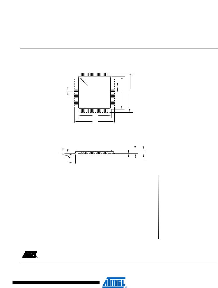
64A
PIN 1 |
|
|
|
|
B |
||||
|
|
|
|||||||
|
|
|
|||||||
e |
|
|
|
PIN 1 IDENTIFIER |
|
|
|
|
|
|
|
|
|
|
|
|
|
||
|
|
|
|
|
|
||||
|
|
|
|
|
|
||||
|
|
|
|
|
|
|
|
||
|
|
|
|
|
|
||||
|
|
|
|
|
|
|
|
|
|
E1 E
D1
D
C  0°~7°
0°~7°
A1 A2 A
A2 A
 L
L
COMMON DIMENSIONS
(Unit of Measure = mm)
Notes:
1.This package conforms to JEDEC reference MS-026, Variation AEB.
2.Dimensions D1 and E1 do not include mold protrusion. Allowable protrusion is 0.25 mm per side. Dimensions D1 and E1 are maximum plastic body size dimensions including mold mismatch.
3. Lead coplanarity is 0.10 mm maximum.
SYMBOL |
MIN |
NOM |
MAX |
NOTE |
A |
– |
– |
1.20 |
|
|
|
|
|
|
A1 |
0.05 |
– |
0.15 |
|
A2 |
0.95 |
1.00 |
1.05 |
|
|
|
|
|
|
D |
15.75 |
16.00 |
16.25 |
|
|
|
|
|
|
D1 |
13.90 |
14.00 |
14.10 |
Note 2 |
|
|
|
|
|
E |
15.75 |
16.00 |
16.25 |
|
|
|
|
|
|
E1 |
13.90 |
14.00 |
14.10 |
Note 2 |
|
|
|
|
|
B |
0.30 |
– |
0.45 |
|
|
|
|
|
|
C |
0.09 |
– |
0.20 |
|
|
|
|
|
|
L |
0.45 |
– |
0.75 |
|
|
|
|
|
|
e |
|
0.80 TYP |
|
|
|
|
|
|
|
2010-10-20
|
|
|
2325 Orchard Parkway |
TITLE |
DRAWING NO. |
REV. |
|
|
|
64A, 64-lead, 14 x 14 mm Body Size, 1.0 mm Body Thickness, |
64A |
C |
|
|
|
|
R San Jose, CA 95131 |
0.8 mm Lead Pitch, Thin Profile Plastic Quad Flat Package (TQFP) |
||
|
|
|
|
|
|
|
|
|
|
|
|
|
|
369
2467X–AVR–06/11
ATmega128
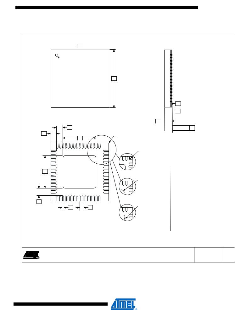
64M1

 D
D 

 Marked Pin# 1 ID
E
TOP VIEW |
|
|
|
K |
|
|
|
L |
|
Pin #1 Corner |
|
D2 |
|
|
|
|
|
|
|
|
1 |
Option A |
Pin #1 |
|
2 |
|
Triangle |
|
|
|
|
|
3 |
|
|
E2 |
|
|
|
|
|
Option B |
Pin #1 |
|
|
|
|
|
|
|
Chamfer |
|
|
|
(C 0.30) |
K |
|
Option C |
Pin #1 |
|
|
|
|
b |
e |
|
Notch |
|
(0.20 R) |
||
|
|
|
BOTTOM VIEW
Notes:
C SEATING PLANE


 A1
A1
A 


 0.08 C
SIDE VIEW
COMMON DIMENSIONS
(Unit of Measure = mm)
SYMBOL |
MIN |
NOM |
MAX |
NOTE |
A |
0.80 |
0.90 |
1.00 |
|
|
|
|
|
|
A1 |
– |
0.02 |
0.05 |
|
b |
0.18 |
0.25 |
0.30 |
|
|
|
|
|
|
D |
8.90 |
9.00 |
9.10 |
|
|
|
|
|
|
D2 |
5.20 |
5.40 |
5.60 |
|
|
|
|
|
|
E |
8.90 |
9.00 |
9.10 |
|
|
|
|
|
|
E2 |
5.20 |
5.40 |
5.60 |
|
|
|
|
|
|
e |
|
0.50 BSC |
|
|
|
|
|
|
|
L |
0.35 |
0.40 |
0.45 |
|
|
|
|
|
|
K |
1.25 |
1.40 |
1.55 |
|
|
|
|
|
|
1.JEDEC Standard MO-220, (SAW Singulation) Fig. 1, VMMD.
2.Dimension and tolerance conform to ASMEY14.5M-1994.
2010-10-19
|
2325 Orchard Parkway |
TITLE |
|
64M1, 64-pad, 9 x 9 x 1.0 mm Body, Lead Pitch 0.50 mm, |
|
|
San Jose, CA 95131 |
|
R |
5.40 mm Exposed Pad, Micro Lead Frame Package (MLF) |
|
|
|
|
DRAWING NO. REV.
64M1 H
370
2467X–AVR–06/11