

- •Features
- •Overview
- •Block Diagram
- •Pin Descriptions
- •Port A (PA7..PA0)
- •Port B (PB7..PB0)
- •Port C (PC7..PC0)
- •Port D (PD7..PD0)
- •Port E (PE7..PE0)
- •Port F (PF7..PF0)
- •Port G (PG4..PG0)
- •RESET
- •XTAL1
- •XTAL2
- •AVCC
- •AREF
- •Resources
- •Data Retention
- •Capacitive touch sensing
- •AVR CPU Core
- •Introduction
- •Status Register
- •Stack Pointer
- •I/O Memory
- •Overview
- •Timing
- •Using all Locations of External Memory Smaller than 64 Kbyte
- •Clock Systems and their Distribution
- •CPU Clock – clkCPU
- •I/O Clock – clkI/O
- •Flash Clock – clkFLASH
- •ADC Clock – clkADC
- •Clock Sources
- •Crystal Oscillator
- •External Clock
- •Idle Mode
- •Power-down Mode
- •Power-save Mode
- •Standby Mode
- •Analog Comparator
- •Brown-out Detector
- •Watchdog Timer
- •Port Pins
- •Resetting the AVR
- •Reset Sources
- •Power-on Reset
- •External Reset
- •Watchdog Reset
- •Watchdog Timer
- •Timed Sequences for Changing the Configuration of the Watchdog Timer
- •Safety Level 0
- •Safety Level 1
- •Safety Level 2
- •Interrupts
- •I/O Ports
- •Introduction
- •Configuring the Pin
- •Reading the Pin Value
- •Unconnected pins
- •Alternate Port Functions
- •Register Description for I/O Ports
- •8-bit Timer/Counter0 with PWM and Asynchronous Operation
- •Overview
- •Registers
- •Definitions
- •Counter Unit
- •Normal Mode
- •Fast PWM Mode
- •8-bit Timer/Counter Register Description
- •Overview
- •Registers
- •Definitions
- •Compatibility
- •Counter Unit
- •Input Capture Unit
- •Noise Canceler
- •Force Output Compare
- •Normal Mode
- •Fast PWM Mode
- •16-bit Timer/Counter Register Description
- •Internal Clock Source
- •Prescaler Reset
- •External Clock Source
- •8-bit Timer/Counter2 with PWM
- •Overview
- •Registers
- •Definitions
- •Counter Unit
- •Normal Mode
- •Fast PWM Mode
- •8-bit Timer/Counter Register Description
- •Output Compare Modulator (OCM1C2)
- •Overview
- •Description
- •Timing Example
- •Slave Mode
- •Master Mode
- •Data Modes
- •USART
- •Dual USART
- •Overview
- •AVR USART vs. AVR UART – Compatibility
- •Clock Generation
- •External Clock
- •Frame Formats
- •Parity Bit Calculation
- •Parity Generator
- •Receiver Error Flags
- •Parity Checker
- •Disabling the Receiver
- •Using MPCM
- •Features
- •TWI Terminology
- •Transferring Bits
- •Address Packet Format
- •Data Packet Format
- •Overview of the TWI Module
- •Scl and SDA Pins
- •Bus Interface Unit
- •Address Match Unit
- •Control Unit
- •Using the TWI
- •Master Receiver Mode
- •Slave Receiver Mode
- •Miscellaneous States
- •Analog Comparator
- •Analog to Digital Converter
- •Features
- •Operation
- •Changing Channel or Reference Selection
- •ADC Input Channels
- •Analog Input Circuitry
- •Features
- •Overview
- •TAP Controller
- •PRIVATE0; $8
- •PRIVATE1; $9
- •PRIVATE2; $A
- •PRIVATE3; $B
- •Bibliography
- •Features
- •System Overview
- •Data Registers
- •Bypass Register
- •Reset Register
- •EXTEST; $0
- •IDCODE; $1
- •AVR_RESET; $C
- •BYPASS; $F
- •Scanning the ADC
- •ATmega128 Boundary-scan Order
- •Application Section
- •Programming Time for Flash when Using SPM
- •Simple Assembly Code Example for a Boot Loader
- •Fuse Bits
- •Latching of Fuses
- •Signature Bytes
- •Calibration Byte
- •Signal Names
- •Chip Erase
- •Reading the Flash
- •Reading the EEPROM
- •Data Polling Flash
- •Data Polling EEPROM
- •AVR_RESET ($C)
- •PROG_ENABLE ($4)
- •Data Registers
- •Reset Register
- •Programming Enable Register
- •Programming Command Register
- •Virtual Flash Page Read Register
- •Performing Chip Erase
- •Reading the Flash
- •Reading the EEPROM
- •Electrical Characteristics
- •Absolute Maximum Ratings*
- •DC Characteristics
- •Speed Grades
- •External Clock Drive Waveforms
- •External Clock Drive
- •Two-wire Serial Interface Characteristics
- •ADC Characteristics
- •External Data Memory Timing
- •Idle Supply Current
- •Pin Pull-up
- •Pin Driver Strength
- •Register Summary
- •Instruction Set Summary
- •Ordering Information
- •Packaging Information
- •Errata
- •ATmega128 Rev. F to M

 ATmega128
IEEE 1149.1 (JTAG) Boundaryscan
Features
•JTAG (IEEE std. 1149.1 Compliant) Interface
•Boundary-scan Capabilities According to the JTAG Standard
•Full Scan of all Port Functions as well as Analog Circuitry having Off-chip Connections
•Supports the Optional IDCODE Instruction
•Additional Public AVR_RESET Instruction to Reset the AVR
System Overview
Data Registers
The Boundary-scan Chain has the capability of driving and observing the logic levels on the digital I/O pins, as well as the boundary between digital and analog logic for analog circuitry having off-chip connections. At system level, all ICs having JTAG capabilities are connected serially by the TDI/TDO signals to form a long Shift Register. An external controller sets up the devices to drive values at their output pins, and observe the input values received from other devices. The controller compares the received data with the expected result. In this way, Boundary-scan provides a mechanism for testing interconnections and integrity of components on Printed Circuits Boards by using the four TAP signals only.
The four IEEE 1149.1 defined mandatory JTAG instructions IDCODE, BYPASS, SAMPLE/PRELOAD, and EXTEST, as well as the AVR specific public JTAG instruction AVR_RESET can be used for testing the Printed Circuit Board. Initial scanning of the data register path will show the ID-code of the device, since IDCODE is the default JTAG instruction. It may be desirable to have the AVR device in reset during Test mode. If not reset, inputs to the device may be determined by the scan operations, and the internal software may be in an undetermined state when exiting the Test mode. Entering Reset, the outputs of any Port Pin will instantly enter the high impedance state, making the HIGHZ instruction redundant. If needed, the BYPASS instruction can be issued to make the shortest possible scan chain through the device. The device can be set in the Reset state either by pulling the external RESET pin low, or issuing the AVR_RESET instruction with appropriate setting of the Reset Data Register.
The EXTEST instruction is used for sampling external pins and loading output pins with data. The data from the output latch will be driven out on the pins as soon as the EXTEST instruction is loaded into the JTAG IR-register. Therefore, the SAMPLE/PRELOAD should also be used for setting initial values to the scan ring, to avoid damaging the board when issuing the EXTEST instruction for the first time. SAMPLE/PRELOAD can also be used for taking a snapshot of the external pins during normal operation of the part.
The JTAGEN fuse must be programmed and the JTD bit in the I/O register MCUCSR must be cleared to enable the JTAG Test Access Port.
When using the JTAG interface for Boundary-scan, using a JTAG TCK clock frequency higher than the internal chip frequency is possible. The chip clock is not required to run.
The data registers relevant for Boundary-scan operations are:
•Bypass Register
•Device Identification Register
•Reset Register
•Boundary-scan Chain
252
2467X–AVR–06/11

 ATmega128
Bypass Register |
The Bypass Register consists of a single Shift Register stage. When the Bypass Register is |
||||||||||
|
selected as path between TDI and TDO, the register is reset to 0 when leaving the Capture-DR |
||||||||||
|
controller state. The Bypass Register can be used to shorten the scan chain on a system when |
||||||||||
|
the other devices are to be tested. |
|
|
|
|
|
|||||
Device Identification |
Figure 122 shows the structure of the Device Identification Register. |
|
|
|
|||||||
Register |
|
|
|
|
|
|
|
|
|
|
|
|
Figure 122. The Format of the Device Identification Register |
|
|
|
|||||||
|
|
|
MSB |
|
|
|
|
|
|
LSB |
|
|
|
|
|
|
|
|
|
|
|
|
|
|
Bit |
31 |
28 |
27 |
|
12 |
11 |
1 |
0 |
|
|
|
|
|
|
|
|
|
|
|
|
|
|
|
Device ID |
Version |
|
Part Number |
|
Manufacturer ID |
|
1 |
|
||
|
|
|
|
|
|
|
|
|
|
|
|
|
|
|
4 bits |
|
16 bits |
|
11 bits |
|
1-bit |
||
Version |
Version is a 4-bit number identifying the revision of the component. The JTAG version number |
||||||||||
|
follows the revision of the device, and wraps around at revision P (0xF). Revision A and Q is |
||||||||||
|
0x0, revision B and R is 0x1 and so on. |
|
|
|
|
|
|||||
Part Number |
The part number is a 16-bit code identifying the component. The JTAG Part Number for Atmel® |
||||||||||
|
AVR® ATmega128 is listed in Table 100. |
|
|
|
|
|
|||||
|
Table 100. AVR JTAG Part Number |
|
|
|
|
|
|||||
|
|
|
|
|
|
|
|
||||
|
Part Number |
|
|
|
JTAG Part Number (Hex) |
|
|
||||
|
|
|
|
|
|
|
|
|
|
||
|
ATmega128 |
|
|
|
|
0x9702 |
|
|
|
||
|
|
|
|
||||||||
Manufacturer ID |
The Manufacturer ID is a 11-bit code identifying the manufacturer. The JTAG manufacturer ID |
||||||||||
|
for ATMEL is listed in Table 101. |
|
|
|
|
|
|||||
|
Table 101. |
Manufacturer ID |
|
|
|
|
|
||||
|
|
|
|
|
|
|
|
||||
|
Manufacturer |
|
|
|
JTAG Manufacturer ID (Hex) |
|
|
||||
|
|
|
|
|
|
|
|
|
|
|
|
|
ATMEL |
|
|
|
|
|
0x01F |
|
|
|
|
Reset Register |
|
|
|
||||||||
The Reset Register is a Test Data Register used to reset the part. Since the AVR tri-states Port |
|||||||||||
|
Pins when reset, the Reset Register can also replace the function of the unimplemented optional |
||||||||||
|
JTAG instruction HIGHZ. |
|
|
|
|
|
|||||
A high value in the Reset Register corresponds to pulling the External Reset low. The part is reset as long as there is a high value present in the Reset Register. Depending on the Fuse settings for the clock options, the part will remain reset for a Reset Time-Out Period (refer to “Clock Sources” on page 36) after releasing the Reset Register. The output from this Data Register is not latched, so the Reset will take place immediately, as shown in Figure 123.
253
2467X–AVR–06/11
 ATmega128
Figure 123. Reset Register
To
TDO
From Other Internal and
External Reset Sources
From |
Internal Reset |
D |
Q |
TDI |
|
ClockDR · AVR_RESET
Boundary-scan Chain The Boundary-scan Chain has the capability of driving and observing the logic levels on the digital I/O pins, as well as the boundary between digital and analog logic for analog circuitry having off-chip connections.
See “Boundary-scan Chain” on page 255 for a complete description.
Boundary-scan
Specific JTAG
Instructions
EXTEST; $0
IDCODE; $1
The Instruction Register is 4-bit wide, supporting up to 16 instructions. Listed below are the JTAG instructions useful for Boundary-scan operation. Note that the optional HIGHZ instruction is not implemented, but all outputs with tri-state capability can be set in high-impedant state by using the AVR_RESET instruction, since the initial state for all port pins is tri-state.
As a definition in this data sheet, the LSB is shifted in and out first for all Shift Registers.
The OPCODE for each instruction is shown behind the instruction name in hex format. The text describes which data register is selected as path between TDI and TDO for each instruction.
Mandatory JTAG instruction for selecting the Boundary-scan Chain as Data Register for testing circuitry external to the AVR package. For port-pins, Pull-up Disable, Output Control, Output Data, and Input Data are all accessible in the scan chain. For Analog circuits having off-chip connections, the interface between the analog and the digital logic is in the scan chain. The contents of the latched outputs of the Boundary-scan chain is driven out as soon as the JTAG IRregister is loaded with the EXTEST instruction.
The active states are:
•Capture-DR: Data on the external pins are sampled into the Boundary-scan Chain.
•Shift-DR: The Internal Scan Chain is shifted by the TCK input.
•Update-DR: Data from the scan chain is applied to output pins.
Optional JTAG instruction selecting the 32-bit ID Register as Data Register. The ID Register consists of a version number, a device number and the manufacturer code chosen by JEDEC. This is the default instruction after power-up.
The active states are:
•Capture-DR: Data in the IDCODE Register is sampled into the Boundary-scan Chain.
•Shift-DR: The IDCODE scan chain is shifted by the TCK input.
254
2467X–AVR–06/11

 ATmega128
SAMPLE_PRELOAD; Mandatory JTAG instruction for pre-loading the output latches and taking a snap-shot of the $2 input/output pins without affecting the system operation. However, the output latched are not
connected to the pins. The Boundary-scan Chain is selected as Data Register.
The active states are:
•Capture-DR: Data on the external pins are sampled into the Boundary-scan Chain.
•Shift-DR: The Boundary-scan Chain is shifted by the TCK input.
•Update-DR: Data from the Boundary-scan Chain is applied to the output latches. However, the output latches are not connected to the pins.
AVR_RESET; $C |
The AVR specific public JTAG instruction for forcing the AVR device into the Reset mode or |
|
releasing the JTAG Reset source. The TAP controller is not reset by this instruction. The one bit |
|
Reset Register is selected as Data Register. Note that the Reset will be active as long as there |
|
is a logic 'one' in the Reset Chain. The output from this chain is not latched. |
The active states are:
•Shift-DR: The Reset Register is shifted by the TCK input.
BYPASS; $F |
Mandatory JTAG instruction selecting the Bypass Register for Data Register. |
The active states are:
•Capture-DR: Loads a logic “0” into the Bypass Register.
•Shift-DR: The Bypass Register cell between TDI and TDO is shifted.
Boundary-scan
Related Register in
I/O Memory
MCU Control and The MCU Control and Status Register contains control bits for general MCU functions, and pro- Status Register – vides information on which reset source caused an MCU Reset.
MCUCSR
Bit |
7 |
6 |
5 |
4 |
3 |
2 |
1 |
0 |
|
|
JTD |
– |
– |
JTRF |
WDRF |
BORF |
EXTRF |
PORF |
MCUCSR |
Read/Write |
R/W |
R |
R |
R/W |
R/W |
R/W |
R/W |
R/W |
|
Initial Value |
0 |
0 |
0 |
|
See Bit Description |
|
|
||
Boundary-scan
Chain
• Bit 7 – JTD: JTAG Interface Disable
When this bit is zero, the JTAG interface is enabled if the JTAGEN fuse is programmed. If this bit is one, the JTAG interface is disabled. In order to avoid unintentional disabling or enabling of the JTAG interface, a timed sequence must be followed when changing this bit: The application software must write this bit to the desired value twice within four cycles to change its value.
If the JTAG interface is left unconnected to other JTAG circuitry, the JTD bit should be set to one. The reason for this is to avoid static current at the TDO pin in the JTAG interface.
• Bit 4 – JTRF: JTAG Reset Flag
This bit is set if a Reset is being caused by a logic one in the JTAG Reset Register selected by the JTAG instruction AVR_RESET. This bit is reset by a Power-on Reset, or by writing a logic zero to the flag.
The Boundary-scan chain has the capability of driving and observing the logic levels on the digital I/O pins, as well as the boundary between digital and analog logic for analog circuitry having off-chip connection.
255
2467X–AVR–06/11
 ATmega128
Scanning the Digital
Port Pins
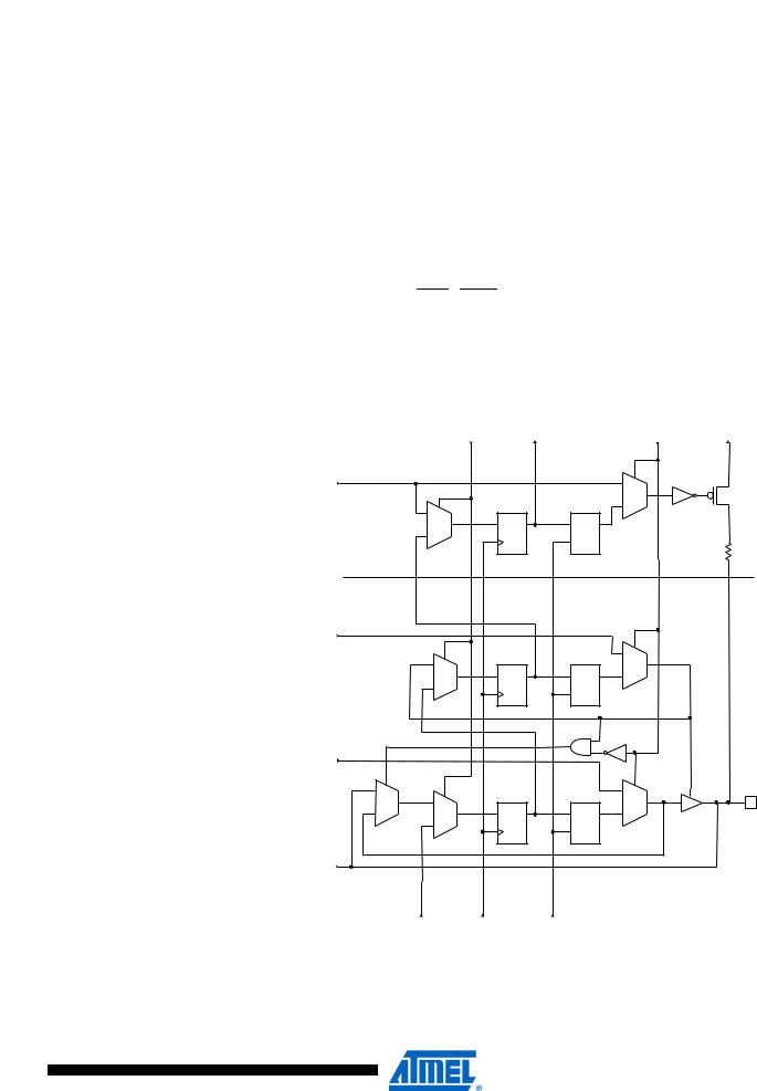
Figure 124 shows the Boundary-scan Cell for a bi-directional port pin with pull-up function. The cell consists of a standard Boundary-scan cell for the Pull-up Enable – PUExn – function, and a bi-directional pin cell that combines the three signals Output Control – OCxn, Output Data – ODxn, and Input Data – IDxn, into only a two-stage Shift Register. The port and pin indexes are not used in the following description
The Boundary-scan logic is not included in the figures in the Data Sheet. Figure 125 shows a simple digital Port Pin as described in the section “I/O Ports” on page 65. The Boundary-scan details from Figure 124 replaces the dashed box in Figure 125.
When no alternate port function is present, the Input Data – ID corresponds to the PINxn Register value (but ID has no synchronizer), Output Data corresponds to the PORT Register, Output Control corresponds to the Data Direction – DD Register, and the Pull-up Enable – PUExn – corresponds to logic expression PUD · DDxn · PORTxn.
Digital alternate port functions are connected outside the dotted box in Figure 125 to make the scan chain read the actual pin value. For Analog function, there is a direct connection from the external pin to the analog circuit, and a scan chain is inserted on the interface between the digital logic and the analog circuitry.
Figure 124. Boundary-scan Cell for Bi-directional Port Pin with Pull-Up Function.
|
ShiftDR |
To Next Cell |
|
|
EXTEST |
|
Pullup Enable (PUE) |
|
|
|
|
0 |
|
|
|
|
|
|
||
|
FF2 |
LD2 |
1 |
|||
|
0 |
|
|
|
||
|
|
|
|
|
||
|
D |
Q |
D |
Q |
|
|
|
1 |
|
G |
|
|
|
|
|
|
|
|
||
Output Control (OC) |
|
|
|
|
|
|
|
FF1 |
LD1 |
0 |
|||
|
0 |
|
|
|
1 |
|
|
D |
Q |
D |
Q |
||
|
|
|||||
|
1 |
|
G |
|
|
|
|
|
|
|
|
||
Output Data (OD) |
|
|
|
|
|
|
0 |
FF0 |
LD0 |
0 |
|||
1 |
0 |
|
|
|
1 |
|
D |
Q |
D |
Q |
|||
|
|
|||||
|
1 |
|
G |
|
|
|
|
|
|
|
|
||
Input Data (ID) |
|
|
|
|
|
|
From Last Cell |
ClockDR |
UpdateDR |
Vcc
Port Pin (PXn)
256
2467X–AVR–06/11
ATmega128
Figure 125. General Port Pin Schematic diagram
See Boundary-Scan description for details!
Boundary-scan and
the Two-wire Interface
PUExn |
PUD |
|
|
|
|
Q |
D |
|
|
|
|
|
DDxn |
|
|
|
|
|
|
Q CLR |
|
|
|
|
|
|
RESET |
WDx |
|
|
OCxn |
|
|
|
|
||
|
|
|
|
|
|
|
|
|
|
|
|
RDx |
|
Pxn |
|
|
Q |
D |
|
BUS |
|
|
|
DATA |
|||
ODxn |
|
|
PORTxn |
|
||
|
|
|
|
|||
|
|
|
Q CLR |
|
|
|
IDxn |
|
|
RESET |
WPx |
|
|
|
|
|
|
|
||
SLEEP |
|
|
|
|
RRx |
|
SYNCHRONIZER |
|
RPx |
|
|||
|
|
|
|
|
|
|
D |
Q |
D |
Q |
|
|
|
|
|
PINxn |
|
|
|
|
L |
Q |
|
Q |
|
|
|
|
|
|
|
|
CLK I/O |
|
PUD: |
PULLUP DISABLE |
WDx: |
WRITE DDRx |
PUExn: |
PULLUP ENABLE for pin Pxn |
RDx: |
READ DDRx |
OCxn: |
OUTPUT CONTROL for pin Pxn |
WPx: |
WRITE PORTx |
ODxn: |
OUTPUT DATA to pin Pxn |
RRx: |
READ PORTx REGISTER |
IDxn: |
INPUT DATA from pin Pxn |
RPx: |
READ PORTx PIN |
SLEEP: |
SLEEP CONTROL |
CLK I/O : |
I/O CLOCK |
The two Two-wire Interface pins SCL and SDA have one additional control signal in the scanchain; Two-wire Interface Enable – TWIEN. As shown in Figure 126, the TWIEN signal enables a tri-state buffer with slew-rate control in parallel with the ordinary digital port pins. A general scan cell as shown in Figure 130 is attached to the TWIEN signal.
Notes: 1. A separate scan chain for the 50 ns spike filter on the input is not provided. The ordinary scan support for digital port pins suffice for connectivity tests. The only reason for having TWIEN in the scan path, is to be able to disconnect the slew-rate control buffer when doing boundaryscan.
2.Make sure the OC and TWIEN signals are not asserted simultaneously, as this will lead to drive contention.
257
2467X–AVR–06/11
 ATmega128
Figure 126. Additional Scan Signal for the Two-wire Interface
PUExn
Scanning the RESET
Pin
|
OCxn |
|
ODxn |
Pxn |
TWIEN |
|
SRC |
|
Slew-rate limited |
|
IDxn |
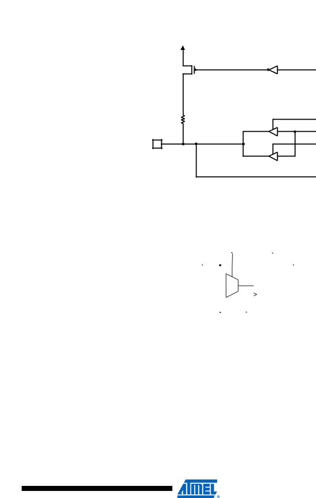
The RESET pin accepts 5V active low logic for standard Reset operation, and 12V active high logic for High Voltage Parallel programming. An observe-only cell as shown in Figure 127 is inserted both for the 5V Reset signal; RSTT, and the 12V Reset signal; RSTHV.
Figure 127. Observe-only Cell
|
|
|
|
|
|
|
To |
||
|
|
|
|
|
|
next |
|||
|
|
ShiftDR |
|
cell |
|||||
From system pin |
|
|
|
|
|
To system logic |
|||
|
|
|
|
|
|
|
|
||
|
|
|
|
|
FF1 |
|
|||
|
|
0 |
|
|
|
|
|
|
|
|
|
|
1 |
|
D |
Q |
|
|
|
|
|
|
|
|
|
|
|
|
|
|
|
|
|
|
|
|
|
|
|
|
|
|
|
|
|
|
|
|
|
|
|
|
|
|
|
|
|
|
|
From ClockDR
previous
cell
Scanning the Clock The Atmel® AVR® devices have many clock options selectable by fuses. These are: Internal RC Pins Oscillator, External RC, External Clock, (High Frequency) Crystal Oscillator, Low-frequency
Crystal Oscillator, and Ceramic Resonator.
Figure 128 shows how each Oscillator with external connection is supported in the scan chain. The Enable signal is supported with a general boundary-scan cell, while the Oscillator/Clock output is attached to an observe-only cell. In addition to the main clock, the Timer Oscillator is scanned in the same way. The output from the internal RC Oscillator is not scanned, as this Oscillator does not have external connections.
258
2467X–AVR–06/11
 ATmega128
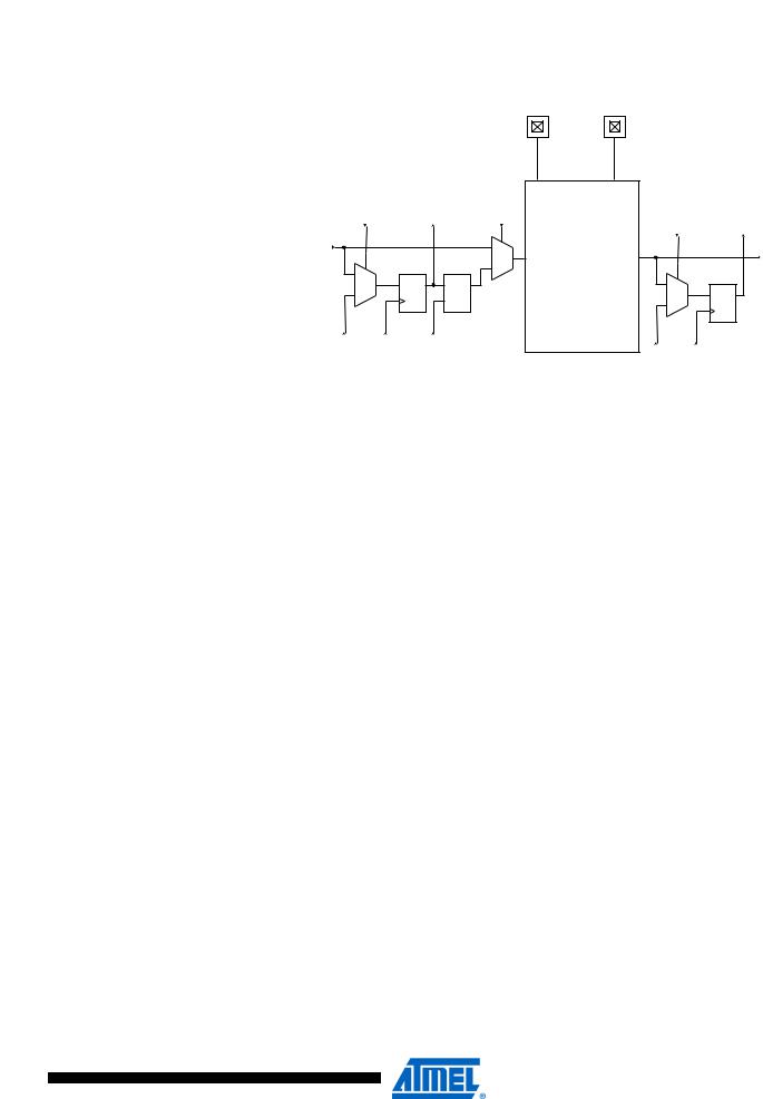
Figure 128. Boundary-scan Cells for Oscillators and Clock Options
XTAL1/TOSC1 XTAL2/TOSC2
Scanning the Analog
Comparator
|
|
|
To |
|
|
|
|
Next |
|
|
ShiftDR |
|
Cell |
EXTEST |
From Digital Logic |
|
|
|
0 |
|
|
|
|
|
|
0 |
|
|
1 |
|
|
|
|
|
|
D |
Q |
D |
Q |
|
1 |
|
G |
|
|
|
|
|
|
From |
ClockDR |
UpdateDR |
|
|
Previous |
|
|
|
|
Cell |
|
|
|
|
Oscillator |
|
To |
|
|
next |
||
|
|
ShiftDR |
cell |
ENABLE |
OUTPUT |
|
To System Logic |
|
|
FF1 |
|
|
|
0 |
|
|
|
D |
Q |
|
|
1 |
|
|
From |
ClockDR |
|
|
Previous |
|
|
|
Cell |
|
|
Table 102 summaries the scan registers for the external clock pin XTAL1, oscillators with XTAL1/XTAL2 connections as well as 32kHz Timer Oscillator.
Table 102. Scan Signals for the Oscillators(1)(2)(3)
|
Scanned Clock |
|
Scanned Clock Line |
Enable signal |
Line |
Clock Option |
when not Used |
|
|
|
|
EXTCLKEN |
EXTCLK (XTAL1) |
External Clock |
0 |
|
|
|
|
OSCON |
OSCCK |
External Crystal |
0 |
|
|
External Ceramic Resonator |
|
|
|
|
|
RCOSCEN |
RCCK |
External RC |
1 |
|
|
|
|
OSC32EN |
OSC32CK |
Low Freq. External Crystal |
0 |
|
|
|
|
TOSKON |
TOSCK |
32kHz Timer Oscillator |
0 |
|
|
|
|
Notes: 1. Do not enable more than one clock source as main clock at a time.
2.Scanning an Oscillator output gives unpredictable results as there is a frequency drift between the Internal Oscillator and the JTAG TCK clock. If possible, scanning an external clock is preferred.
3.The clock configuration is programmed by fuses. As a fuse is not changed run-time, the clock configuration is considered fixed for a given application. The user is advised to scan the same clock option as to be used in the final system. The enable signals are supported in the scan chain because the system logic can disable clock options in sleep modes, thereby disconnecting the Oscillator pins from the scan path if not provided. The INTCAP fuses are not supported in the scan-chain, so the boundary scan chain can not make a XTAL Oscillator requiring internal capacitors to run unless the fuse is correctly programmed.
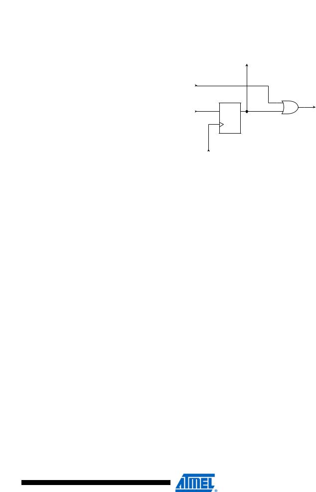
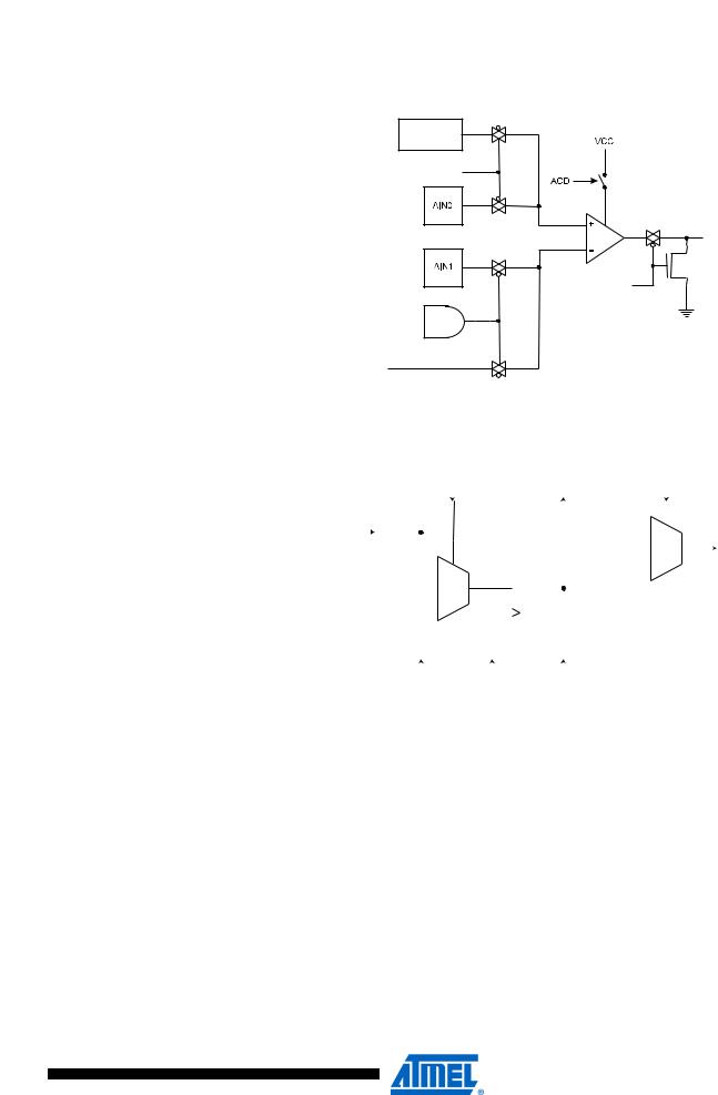
The relevant Comparator signals regarding Boundary-scan are shown in Figure 129. The Boundary-scan cell from Figure 130 is attached to each of these signals. The signals are described in Table 103.
The Comparator need not be used for pure connectivity testing, since all analog inputs are shared with a digital port pin as well.
259
2467X–AVR–06/11
 ATmega128
Figure 129. Analog comparator
BANDGAP
REFERENCE
ACBG
ACO
AC_IDLE
ACME
ADCEN 
ADC MULTIPLEXER
OUTPUT
Figure 130. General Boundary-scan Cell used for Signals for Comparator and ADC
|
|
|
|
|
|
|
To |
|
|
|
|
|
|
|
|
|
|
|
|
|
|
|
Next |
|
|
|
|
|
|
|
|
||
|
|
ShiftDR |
Cell |
|
|
EXTEST |
|
|||||||||
From Digital Logic/ |
|
|
|
|
|
|
|
|
|
|
|
|
|
|||
|
|
|
|
|
|
|
|
|
|
|
|
|
|
|
|
|
|
|
|
|
|
|
|
|
|
|
|
|
|
|
|
|
|
|
|
|
|
|
|
0 |
|
|
|
|||||||
From Analog Ciruitry |
|
|
|
|
|
|
|
|
|
To Analog Circuitry/ |
||||||
|
|
|
|
|
|
|
|
|
|
|
|
|
|
|||
|
|
|
0 |
|
|
|
|
|
|
|
1 |
|
|
To Digital Logic |
||
|
|
|
|
|
|
|
|
|
|
|
|
|
||||
|
|
|
D |
Q |
|
|
D Q |
|
|
|
|
|
|
|
||
|
|
|
1 |
|
|
|
|
|
|
|
|
|
|
|||
|
|
|
|
|
|
|
|
|
|
|
|
|
||||
|
|
|
|
|
|
|
|
G |
|
|
|
|
|
|
|
|
|
|
|
|
|
|
|
|
|
|
|
|
|
|
|
|
|
|
|
|
|
|
|
|
|
|
|
|
|
|
|
|
|
|
|
|
|
|
|
|
|
|
|
|
|
|
|
|
|
|
|
|
|
|
|
|
|
|
|
|
|
|
|
|
|
|
|
|
From ClockDR UpdateDR
Previous
Cell
260
2467X–AVR–06/11