

- •Features
- •Overview
- •Block Diagram
- •Pin Descriptions
- •Port A (PA7..PA0)
- •Port B (PB7..PB0)
- •Port C (PC7..PC0)
- •Port D (PD7..PD0)
- •Port E (PE7..PE0)
- •Port F (PF7..PF0)
- •Port G (PG4..PG0)
- •RESET
- •XTAL1
- •XTAL2
- •AVCC
- •AREF
- •Resources
- •Data Retention
- •Capacitive touch sensing
- •AVR CPU Core
- •Introduction
- •Status Register
- •Stack Pointer
- •I/O Memory
- •Overview
- •Timing
- •Using all Locations of External Memory Smaller than 64 Kbyte
- •Clock Systems and their Distribution
- •CPU Clock – clkCPU
- •I/O Clock – clkI/O
- •Flash Clock – clkFLASH
- •ADC Clock – clkADC
- •Clock Sources
- •Crystal Oscillator
- •External Clock
- •Idle Mode
- •Power-down Mode
- •Power-save Mode
- •Standby Mode
- •Analog Comparator
- •Brown-out Detector
- •Watchdog Timer
- •Port Pins
- •Resetting the AVR
- •Reset Sources
- •Power-on Reset
- •External Reset
- •Watchdog Reset
- •Watchdog Timer
- •Timed Sequences for Changing the Configuration of the Watchdog Timer
- •Safety Level 0
- •Safety Level 1
- •Safety Level 2
- •Interrupts
- •I/O Ports
- •Introduction
- •Configuring the Pin
- •Reading the Pin Value
- •Unconnected pins
- •Alternate Port Functions
- •Register Description for I/O Ports
- •8-bit Timer/Counter0 with PWM and Asynchronous Operation
- •Overview
- •Registers
- •Definitions
- •Counter Unit
- •Normal Mode
- •Fast PWM Mode
- •8-bit Timer/Counter Register Description
- •Overview
- •Registers
- •Definitions
- •Compatibility
- •Counter Unit
- •Input Capture Unit
- •Noise Canceler
- •Force Output Compare
- •Normal Mode
- •Fast PWM Mode
- •16-bit Timer/Counter Register Description
- •Internal Clock Source
- •Prescaler Reset
- •External Clock Source
- •8-bit Timer/Counter2 with PWM
- •Overview
- •Registers
- •Definitions
- •Counter Unit
- •Normal Mode
- •Fast PWM Mode
- •8-bit Timer/Counter Register Description
- •Output Compare Modulator (OCM1C2)
- •Overview
- •Description
- •Timing Example
- •Slave Mode
- •Master Mode
- •Data Modes
- •USART
- •Dual USART
- •Overview
- •AVR USART vs. AVR UART – Compatibility
- •Clock Generation
- •External Clock
- •Frame Formats
- •Parity Bit Calculation
- •Parity Generator
- •Receiver Error Flags
- •Parity Checker
- •Disabling the Receiver
- •Using MPCM
- •Features
- •TWI Terminology
- •Transferring Bits
- •Address Packet Format
- •Data Packet Format
- •Overview of the TWI Module
- •Scl and SDA Pins
- •Bus Interface Unit
- •Address Match Unit
- •Control Unit
- •Using the TWI
- •Master Receiver Mode
- •Slave Receiver Mode
- •Miscellaneous States
- •Analog Comparator
- •Analog to Digital Converter
- •Features
- •Operation
- •Changing Channel or Reference Selection
- •ADC Input Channels
- •Analog Input Circuitry
- •Features
- •Overview
- •TAP Controller
- •PRIVATE0; $8
- •PRIVATE1; $9
- •PRIVATE2; $A
- •PRIVATE3; $B
- •Bibliography
- •Features
- •System Overview
- •Data Registers
- •Bypass Register
- •Reset Register
- •EXTEST; $0
- •IDCODE; $1
- •AVR_RESET; $C
- •BYPASS; $F
- •Scanning the ADC
- •ATmega128 Boundary-scan Order
- •Application Section
- •Programming Time for Flash when Using SPM
- •Simple Assembly Code Example for a Boot Loader
- •Fuse Bits
- •Latching of Fuses
- •Signature Bytes
- •Calibration Byte
- •Signal Names
- •Chip Erase
- •Reading the Flash
- •Reading the EEPROM
- •Data Polling Flash
- •Data Polling EEPROM
- •AVR_RESET ($C)
- •PROG_ENABLE ($4)
- •Data Registers
- •Reset Register
- •Programming Enable Register
- •Programming Command Register
- •Virtual Flash Page Read Register
- •Performing Chip Erase
- •Reading the Flash
- •Reading the EEPROM
- •Electrical Characteristics
- •Absolute Maximum Ratings*
- •DC Characteristics
- •Speed Grades
- •External Clock Drive Waveforms
- •External Clock Drive
- •Two-wire Serial Interface Characteristics
- •ADC Characteristics
- •External Data Memory Timing
- •Idle Supply Current
- •Pin Pull-up
- •Pin Driver Strength
- •Register Summary
- •Instruction Set Summary
- •Ordering Information
- •Packaging Information
- •Errata
- •ATmega128 Rev. F to M

 ATmega128
Electrical Characteristics
Note: Typical values contained in this data sheet are based on simulations and characterization of other AVR microcontrollers manufactured on the same process technology. Min and Max values will be available after the device is characterized.
Absolute Maximum Ratings*
Operating Temperature.................................. -55°C to +125°C |
*NOTICE: Stresses beyond those listed under “Absolute |
||||
|
|
|
|
|
Maximum Ratings” may cause permanent dam- |
Storage Temperature ..................................... -65°C to +150°C |
age to the device. This is a stress rating only and |
||||
|
|
|
|
|
functional operation of the device at these or |
Voltage on any Pin except |
RESET |
|
other conditions beyond those indicated in the |
||
with respect to Ground ................................-0.5V to VCC+0.5V |
operational sections of this specification is not |
||||
Voltage on |
|
with respect to Ground......-0.5V to +13.0V |
implied. Exposure to absolute maximum rating |
||
RESET |
conditions for extended periods may affect device |
||||
Maximum Operating Voltage ............................................ 6.0V |
reliability. |
||||
|
|||||
DC Current per I/O Pin ............................................... 40.0 mA |
|
||||
DC Current VCC and GND Pins..................... 200.0 - 400.0mA |
|
||||
|
|
|
|
|
|
DC Characteristics
TA = -40°C to 85°C, VCC = 2.7V to 5.5V (unless otherwise noted)
Symbol |
|
Parameter |
Condition |
|
Min |
Typ |
Max |
Units |
|||||
|
|
|
|
|
|
|
|
|
|
|
|||
|
|
Input Low Voltage except |
|
|
|
|
|
|
(1) |
|
|||
VIL |
|
XTAL1 and |
|
pins |
VCC = 2.7V - 5.5V |
-0.5 |
|
0.2 VCC |
|
||||
RESET |
|
|
|||||||||||
|
|
Input High Voltage except |
|
|
|
|
(2) |
|
|
|
|||
VIH |
|
XTAL1 and |
|
pins |
VCC = 2.7V - 5.5V |
0.6 VCC |
|
VCC + 0.5 |
|
||||
RESET |
|
|
|||||||||||
VIL1 |
|
Input Low Voltage |
VCC = 2.7V - 5.5V |
-0.5 |
|
(1) |
|
||||||
|
XTAL1 pin |
|
0.1 VCC |
|
|||||||||
|
|
|
|
|
|
|
|
|
V |
||||
|
|
|
|
|
|
|
|
|
|
|
|
|
|
|
|
Input High Voltage XTAL1 |
VCC = 2.7V - 5.5V |
(2) |
|
|
|||||||
|
|
|
|
|
|||||||||
VIH1 |
|
pin |
0.7 VCC |
|
VCC + 0.5 |
|
|||||||
|
|
Input Low Voltage |
|
|
|
|
|
|
(1) |
|
|||
VIL2 |
|
|
|
|
|
VCC = 2.7V - 5.5V |
-0.5 |
|
0.2 VCC |
|
|||
RESET pin |
|
|
|||||||||||
|
|
|
|
|
|
|
|
|
|
||||
|
|
|
|
|
|
|
|
|
|
|
|||
|
|
Input High Voltage |
|
|
|
|
(2) |
|
|
|
|||
VIH2 |
|
|
|
|
|
VCC = 2.7V - 5.5V |
0.85 VCC |
|
VCC + 0.5 |
|
|||
RESET pin |
|
|
|||||||||||
|
|
|
|
|
|
|
|
|
|
||||
|
|
|
|
|
|
|
|
|
|
|
|||
|
|
Output Low Voltage(3) |
I |
OL |
= 20mA, V |
= 5V |
|
|
0.7 |
V |
|||
VOL |
|
|
|
|
|
|
|
CC |
|
|
|
|
|
|
(Ports A,B,C,D, E, F, G) |
IOL = 10mA, VCC = 3V |
|
|
0.5 |
V |
|||||||
|
|
|
|
||||||||||
VOH |
|
Output High Voltage(4) |
IOH = -20mA, VCC = 5V |
4.2 |
|
|
V |
||||||
|
(Ports A,B,C,D, E, F, G) |
IOH = -10mA, VCC = 3V |
2.2 |
|
|
V |
|||||||
|
|
|
|
||||||||||
IIL |
|
Input Leakage |
Vcc = 5.5V, pin low |
|
|
1.0 |
|
||||||
|
Current I/O Pin |
(absolute value) |
|
|
µA |
||||||||
IIH |
|
Input Leakage |
Vcc = 5.5V, pin high |
|
|
1.0 |
|||||||
|
|
|
|
||||||||||
|
Current I/O Pin |
(absolute value) |
|
|
|
||||||||
RRST |
|
Reset Pull-up Resistor |
|
|
|
|
30 |
|
85 |
|
|||
RPEN |
|
PEN Pull-up Resistor |
|
|
|
|
30 |
|
60 |
kΩ |
|||
RPU |
|
I/O Pin Pull-up Resistor |
|
|
|
|
20 |
|
50 |
|
|||
318
2467X–AVR–06/11

 ATmega128
TA = -40°C to 85°C, VCC = 2.7V to 5.5V (unless otherwise noted) |
(Continued) |
|
|
|
||||
Symbol |
Parameter |
Condition |
|
Min |
|
Typ |
Max |
Units |
|
|
|
|
|
|
|
|
|
|
|
Active 4MHz, VCC = 3V |
|
|
|
5 |
5.5 |
|
|
|
(ATmega128L) |
|
|
|
|
|
|
|
|
Active 8MHz, VCC = 5V |
|
|
|
17 |
19 |
|
|
Power Supply Current |
(ATmega128) |
|
|
|
|
|
mA |
ICC |
Idle 4MHz, VCC = 3V |
|
|
|
2 |
2.5 |
||
|
|
|
|
|
||||
|
(ATmega128L) |
|
|
|
|
|
|
|
|
|
Idle 8MHz, VCC = 5V |
|
|
|
8 |
11 |
|
|
|
(ATmega128) |
|
|
|
|
|
|
|
Power-down mode |
WDT enabled, VCC = 3V |
|
|
|
< 15 |
25 |
µA |
|
WDT disabled, VCC = 3V |
|
|
|
< 5 |
10 |
||
|
|
|
|
|
|
|||
VACIO |
Analog Comparator |
VCC = 5V |
|
|
|
|
40 |
mV |
Input Offset Voltage |
Vin = VCC/2 |
|
|
|
|
|||
|
|
|
|
|
|
|
||
IACLK |
Analog Comparator |
VCC = 5V |
|
-50 |
|
|
50 |
nA |
Input Leakage Current |
Vin = VCC/2 |
|
|
|
||||
|
|
|
|
|
|
|
||
tACPD |
Analog Comparator |
VCC = 2.7V |
|
|
|
750 |
|
ns |
Propagation Delay |
VCC = 5.0V |
|
|
|
500 |
|
||
|
|
|
|
|
|
|||
Notes: 1. |
“Max” means the highest value where the pin is guaranteed to be read as low |
|
|
|
||||
2.“Min” means the lowest value where the pin is guaranteed to be read as high
3.Although each I/O port can sink more than the test conditions (20mA at VCC = 5V, 10mA at VCC = 3V) under steady state conditions (non-transient), the following must be observed:
TQFP and QFN/MLF Package:
1] The sum of all IOL, for all ports, should not exceed 400mA.
2] The sum of all IOL, for ports A0 - A7, G2, C3 - C7 should not exceed 100mA.
3] The sum of all IOL, for ports C0 - C2, G0 - G1, D0 - D7, XTAL2 should not exceed 100mA. 4] The sum of all IOL, for ports B0 - B7, G3 - G4, E0 - E7 should not exceed 100mA.
5] The sum of all IOL, for ports F0 - F7, should not exceed 100mA.
If IOL exceeds the test condition, VOL may exceed the related specification. Pins are not guaranteed to sink current greater than the listed test condition.
4.Although each I/O port can source more than the test conditions (20mA at Vcc = 5V, 10mA at Vcc = 3V) under steady state conditions (non-transient), the following must be observed:
TQFP and QFN/MLF Package:
1] The sum of all IOH, for all ports, should not exceed 400mA.
2] The sum of all IOH, for ports A0 - A7, G2, C3 - C7 should not exceed 100mA.
3] The sum of all IOH, for ports C0 - C2, G0 - G1, D0 - D7, XTAL2 should not exceed 100mA. 4] The sum of all IOH, for ports B0 - B7, G3 - G4, E0 - E7 should not exceed 100mA.
5] The sum of all IOH, for ports F0 - F7, should not exceed 100mA.
If IOH exceeds the test condition, VOH may exceed the related specification. Pins are not guaranteed to source current greater than the listed test condition.
319
2467X–AVR–06/11
ATmega128
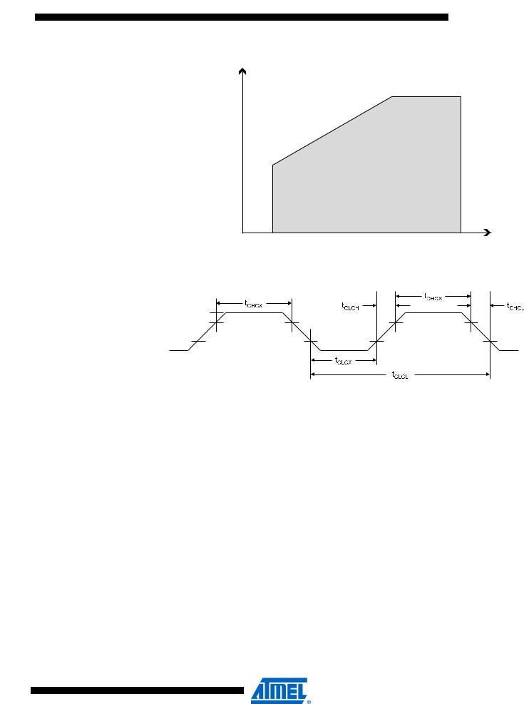
Speed Grades
Figure 152. Maximum frequency vs. VCC
16MHz |
|
|
8MHz |
Safe Operating Area |
|
|
|
|
2.7V |
4.5V |
5.5V |
External Clock
Drive Waveforms
Figure 153. External Clock Drive Waveforms
External Clock
Drive
VIH1
VIL1
Table 131. External Clock Drive
|
|
VCC = 2.7V to 5.5V |
VCC = 4.5V to 5.5V |
|
||
Symbol |
Parameter |
Min |
Max |
Min |
Max |
Units |
|
|
|
|
|
|
|
1/tCLCL |
Oscillator Frequency |
0 |
8 |
0 |
16 |
MHz |
tCLCL |
Clock Period |
125 |
|
62.5 |
|
ns |
tCHCX |
High Time |
50 |
|
25 |
|
ns |
tCLCX |
Low Time |
50 |
|
25 |
|
ns |
tCLCH |
Rise Time |
|
1.6 |
|
0.5 |
μs |
tCHCL |
Fall Time |
|
1.6 |
|
0.5 |
μs |
|
Change in period from |
|
|
|
|
|
|
one clock cycle to the |
|
2 |
|
2 |
% |
tCLCL |
next |
|
|
|
|
|
320
2467X–AVR–06/11
 ATmega128
Table 132. External RC Oscillator, Typical Frequencies
R [kΩ](1) |
C [pF] |
f(2) |
33 |
22 |
650kHz |
|
|
|
10 |
22 |
2.0MHz |
|
|
|
Notes: 1. R should be in the range 3kΩ - 100kΩ, and C should be at least 20pF. The C values given in the table includes pin capacitance. This will vary with package type.
2. The frequency will vary with package type and board layout.
321
2467X–AVR–06/11