

- •Features
- •Overview
- •Block Diagram
- •Pin Descriptions
- •Port A (PA7..PA0)
- •Port B (PB7..PB0)
- •Port C (PC7..PC0)
- •Port D (PD7..PD0)
- •Port E (PE7..PE0)
- •Port F (PF7..PF0)
- •Port G (PG4..PG0)
- •RESET
- •XTAL1
- •XTAL2
- •AVCC
- •AREF
- •Resources
- •Data Retention
- •Capacitive touch sensing
- •AVR CPU Core
- •Introduction
- •Status Register
- •Stack Pointer
- •I/O Memory
- •Overview
- •Timing
- •Using all Locations of External Memory Smaller than 64 Kbyte
- •Clock Systems and their Distribution
- •CPU Clock – clkCPU
- •I/O Clock – clkI/O
- •Flash Clock – clkFLASH
- •ADC Clock – clkADC
- •Clock Sources
- •Crystal Oscillator
- •External Clock
- •Idle Mode
- •Power-down Mode
- •Power-save Mode
- •Standby Mode
- •Analog Comparator
- •Brown-out Detector
- •Watchdog Timer
- •Port Pins
- •Resetting the AVR
- •Reset Sources
- •Power-on Reset
- •External Reset
- •Watchdog Reset
- •Watchdog Timer
- •Timed Sequences for Changing the Configuration of the Watchdog Timer
- •Safety Level 0
- •Safety Level 1
- •Safety Level 2
- •Interrupts
- •I/O Ports
- •Introduction
- •Configuring the Pin
- •Reading the Pin Value
- •Unconnected pins
- •Alternate Port Functions
- •Register Description for I/O Ports
- •8-bit Timer/Counter0 with PWM and Asynchronous Operation
- •Overview
- •Registers
- •Definitions
- •Counter Unit
- •Normal Mode
- •Fast PWM Mode
- •8-bit Timer/Counter Register Description
- •Overview
- •Registers
- •Definitions
- •Compatibility
- •Counter Unit
- •Input Capture Unit
- •Noise Canceler
- •Force Output Compare
- •Normal Mode
- •Fast PWM Mode
- •16-bit Timer/Counter Register Description
- •Internal Clock Source
- •Prescaler Reset
- •External Clock Source
- •8-bit Timer/Counter2 with PWM
- •Overview
- •Registers
- •Definitions
- •Counter Unit
- •Normal Mode
- •Fast PWM Mode
- •8-bit Timer/Counter Register Description
- •Output Compare Modulator (OCM1C2)
- •Overview
- •Description
- •Timing Example
- •Slave Mode
- •Master Mode
- •Data Modes
- •USART
- •Dual USART
- •Overview
- •AVR USART vs. AVR UART – Compatibility
- •Clock Generation
- •External Clock
- •Frame Formats
- •Parity Bit Calculation
- •Parity Generator
- •Receiver Error Flags
- •Parity Checker
- •Disabling the Receiver
- •Using MPCM
- •Features
- •TWI Terminology
- •Transferring Bits
- •Address Packet Format
- •Data Packet Format
- •Overview of the TWI Module
- •Scl and SDA Pins
- •Bus Interface Unit
- •Address Match Unit
- •Control Unit
- •Using the TWI
- •Master Receiver Mode
- •Slave Receiver Mode
- •Miscellaneous States
- •Analog Comparator
- •Analog to Digital Converter
- •Features
- •Operation
- •Changing Channel or Reference Selection
- •ADC Input Channels
- •Analog Input Circuitry
- •Features
- •Overview
- •TAP Controller
- •PRIVATE0; $8
- •PRIVATE1; $9
- •PRIVATE2; $A
- •PRIVATE3; $B
- •Bibliography
- •Features
- •System Overview
- •Data Registers
- •Bypass Register
- •Reset Register
- •EXTEST; $0
- •IDCODE; $1
- •AVR_RESET; $C
- •BYPASS; $F
- •Scanning the ADC
- •ATmega128 Boundary-scan Order
- •Application Section
- •Programming Time for Flash when Using SPM
- •Simple Assembly Code Example for a Boot Loader
- •Fuse Bits
- •Latching of Fuses
- •Signature Bytes
- •Calibration Byte
- •Signal Names
- •Chip Erase
- •Reading the Flash
- •Reading the EEPROM
- •Data Polling Flash
- •Data Polling EEPROM
- •AVR_RESET ($C)
- •PROG_ENABLE ($4)
- •Data Registers
- •Reset Register
- •Programming Enable Register
- •Programming Command Register
- •Virtual Flash Page Read Register
- •Performing Chip Erase
- •Reading the Flash
- •Reading the EEPROM
- •Electrical Characteristics
- •Absolute Maximum Ratings*
- •DC Characteristics
- •Speed Grades
- •External Clock Drive Waveforms
- •External Clock Drive
- •Two-wire Serial Interface Characteristics
- •ADC Characteristics
- •External Data Memory Timing
- •Idle Supply Current
- •Pin Pull-up
- •Pin Driver Strength
- •Register Summary
- •Instruction Set Summary
- •Ordering Information
- •Packaging Information
- •Errata
- •ATmega128 Rev. F to M
 ATmega128
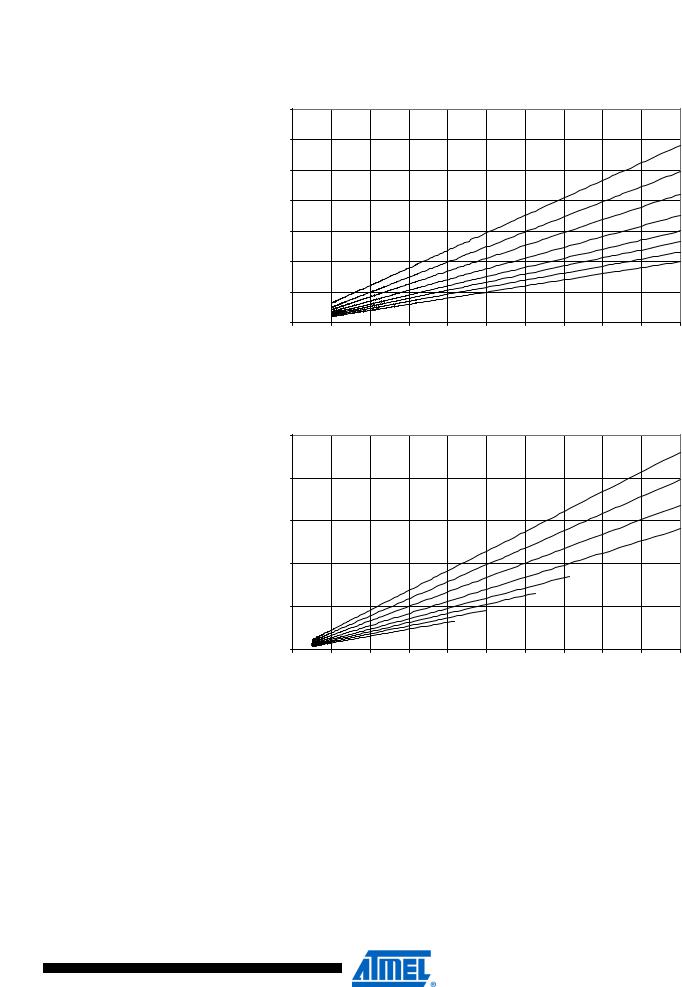
Idle Supply Current |
Figure 168. Idle Supply Current vs. Frequency (0.1 - 1.0MHz) |
|
1.4 |
|
|
|
|
|
|
|
|
|
|
|
1.2 |
|
|
|
|
|
|
|
|
|
5.5V |
|
|
|
|
|
|
|
|
|
|
|
|
|
1 |
|
|
|
|
|
|
|
|
|
5.0V |
(mA) |
0.8 |
|
|
|
|
|
|
|
|
|
4.5V |
|
|
|
|
|
|
|
|
|
|
||
|
|
|
|
|
|
|
|
|
|
4.0V |
|
CC |
0.6 |
|
|
|
|
|
|
|
|
|
3.6V |
I |
|
|
|
|
|
|
|
|
|
||
|
|
|
|
|
|
|
|
|
|
||
|
|
|
|
|
|
|
|
|
|
|
3.3V |
|
|
|
|
|
|
|
|
|
|
|
3.0V |
|
0.4 |
|
|
|
|
|
|
|
|
|
2.7V |
|
0.2 |
|
|
|
|
|
|
|
|
|
|
|
0 |
|
|
|
|
|
|
|
|
|
|
|
0 |
0.1 |
0.2 |
0.3 |
0.4 |
0.5 |
0.6 |
0.7 |
0.8 |
0.9 |
1 |
Frequency (MHz)
Figure 169. Idle Supply Current vs. Frequency (1 - 20MHz)
25 |
|
|
|
|
|
|
|
|
|
|
|
|
|
|
|
|
|
|
|
|
5.5V |
20 |
|
|
|
|
|
|
|
|
|
5.0V |
|
|
|
|
|
|
|
|
|
|
4.5V |
15 |
|
|
|
|
|
|
|
|
|
4.0V |
(mA) |
|
|
|
|
|
|
|
|
|
|
|
|
|
|
|
|
|
|
|
|
|
CC |
|
|
|
|
|
|
|
|
|
|
I |
|
|
|
|
|
|
|
|
|
|
10 |
|
|
|
|
|
|
|
3.6V |
|
|
|
|
|
|
|
|
|
|
|
|
|
5 |
|
|
|
|
|
|
3.3V |
|
|
|
|
|
|
|
|
3.0V |
|
|
|
|
|
|
|
|
|
|
2.7V |
|
|
|
|
|
|
|
|
|
|
|
|
|
|
|
|
0 |
|
|
|
|
|
|
|
|
|
|
0 |
2 |
4 |
6 |
8 |
10 |
12 |
14 |
16 |
18 |
20 |
Frequency (MHz)
337
2467X–AVR–06/11
 ATmega128
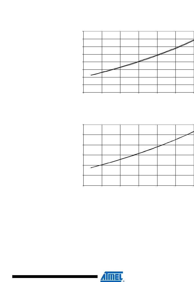
Figure 170. Idle Supply Current vs. VCC (Internal RC Oscillator, 1MHz)
|
1.6 |
|
|
|
|
|
|
|
1.4 |
|
|
|
|
|
85 °C |
|
|
|
|
|
|
25 °C |
|
|
|
|
|
|
|
|
|
|
1.2 |
|
|
|
|
|
-40 °C |
|
|
|
|
|
|
|
|
|
1 |
|
|
|
|
|
|
(mA) |
0.8 |
|
|
|
|
|
|
CC |
|
|
|
|
|
|
|
I |
|
|
|
|
|
|
|
|
0.6 |
|
|
|
|
|
|
|
0.4 |
|
|
|
|
|
|
|
0.2 |
|
|
|
|
|
|
|
0 |
|
|
|
|
|
|
|
2.5 |
3 |
3.5 |
4 |
4.5 |
5 |
5.5 |
VCC (V)
Figure 171. Idle Supply Current vs. VCC (Internal RC Oscillator, 2MHz)
|
3 |
|
|
|
|
|
|
|
|
|
|
|
|
|
85 °C |
|
|
|
|
|
|
|
25 °C |
|
2.5 |
|
|
|
|
|
-40 °C |
|
2 |
|
|
|
|
|
|
(mA) |
1.5 |
|
|
|
|
|
|
CC |
|
|
|
|
|
|
|
I |
|
|
|
|
|
|
|
|
1 |
|
|
|
|
|
|
|
0.5 |
|
|
|
|
|
|
|
0 |
|
|
|
|
|
|
|
2.5 |
3 |
3.5 |
4 |
4.5 |
5 |
5.5 |
VCC (V)
338
2467X–AVR–06/11

 ATmega128
Figure 172. Idle Supply Current vs. VCC (Internal RC Oscillator, 4MHz)
|
6 |
|
|
|
|
|
-40 °C |
|
|
|
|
|
|
|
|
|
|
|
|
|
|
|
25 °C |
|
5 |
|
|
|
|
|
85 °C |
|
|
|
|
|
|
|
|
|
4 |
|
|
|
|
|
|
(mA) |
3 |
|
|
|
|
|
|
CC |
|
|
|
|
|
|
|
I |
|
|
|
|
|
|
|
|
2 |
|
|
|
|
|
|
|
1 |
|
|
|
|
|
|
|
0 |
|
|
|
|
|
|
|
2.5 |
3 |
3.5 |
4 |
4.5 |
5 |
5.5 |
VCC (V)
Figure 173. Idle Supply Current vs. VCC (Internal RC Oscillator, 8MHz)
|
12 |
|
|
|
|
|
-40 °C |
|
|
|
|
|
|
|
|
|
|
|
|
|
|
|
25 °C |
|
10 |
|
|
|
|
|
85 °C |
|
|
|
|
|
|
|
|
|
8 |
|
|
|
|
|
|
(mA) |
6 |
|
|
|
|
|
|
CC |
|
|
|
|
|
|
|
I |
|
|
|
|
|
|
|
|
4 |
|
|
|
|
|
|
|
2 |
|
|
|
|
|
|
|
0 |
|
|
|
|
|
|
|
2.5 |
3 |
3.5 |
4 |
4.5 |
5 |
5.5 |
VCC (V)
339
2467X–AVR–06/11
 ATmega128
Power-down Supply
Current
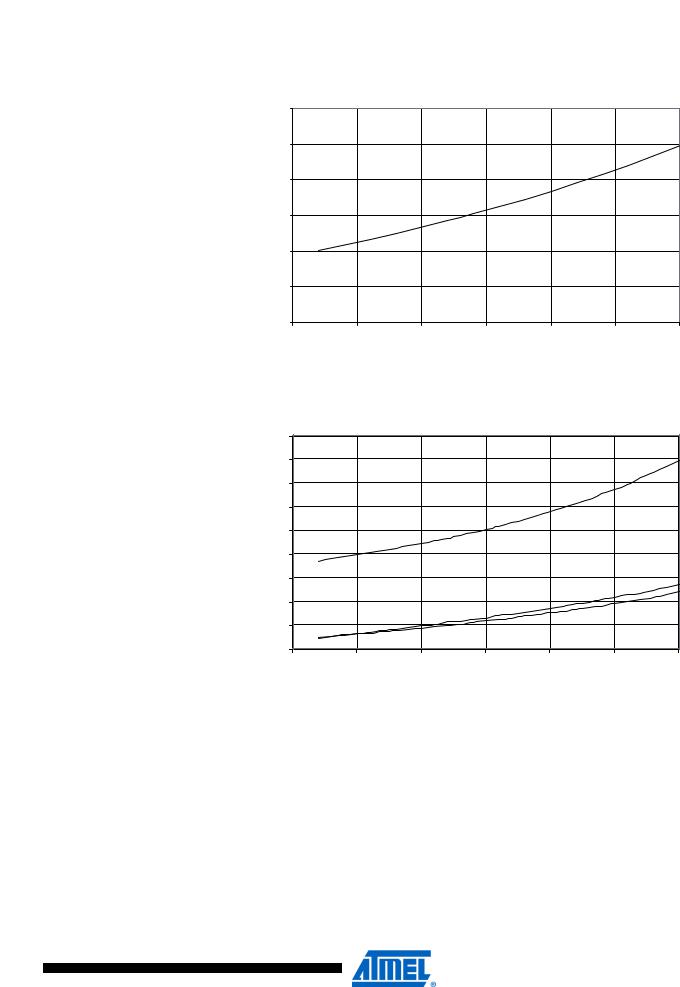
Figure 174. Idle Supply Current vs. VCC (32kHz External Oscillator)
|
60 |
|
|
|
|
|
|
|
50 |
|
|
|
|
|
25 °C |
|
40 |
|
|
|
|
|
|
(uA) |
30 |
|
|
|
|
|
|
CC |
|
|
|
|
|
|
|
|
|
|
|
|
|
|
|
I |
|
|
|
|
|
|
|
|
20 |
|
|
|
|
|
|
|
10 |
|
|
|
|
|
|
|
0 |
|
|
|
|
|
|
|
2.5 |
3 |
3.5 |
4 |
4.5 |
5 |
5.5 |
VCC (V)
Figure 175. Power-down Supply Current vs. VCC (Watchdog Timer Disabled)
|
4.5 |
|
|
|
|
|
|
|
|
4 |
|
|
|
|
|
85 |
°C |
|
3.5 |
|
|
|
|
|
|
|
|
3 |
|
|
|
|
|
|
|
(uA) |
2.5 |
|
|
|
|
|
|
|
|
|
|
|
|
|
|
|
|
CC |
2 |
|
|
|
|
|
|
|
I |
|
|
|
|
|
|
|
|
|
1.5 |
|
|
|
|
|
-40 |
°C |
|
1 |
|
|
|
|
|
25 |
°C |
|
|
|
|
|
|
|
|
|
|
0.5 |
|
|
|
|
|
|
|
|
0 |
|
|
|
|
|
|
|
|
2.5 |
3 |
3.5 |
4 |
4.5 |
5 |
5.5 |
|
VCC (V)
340
2467X–AVR–06/11
 ATmega128
Power-save Supply
Current
Figure 176. Power-down Supply Current vs. VCC (Watchdog Timer Enabled)
|
35 |
|
|
|
|
|
|
|
|
30 |
|
|
|
|
|
85 |
°C |
|
|
|
|
|
|
|
25 |
°C |
|
25 |
|
|
|
|
|
-40 |
°C |
|
|
|
|
|
|
|
|
|
(uA) |
20 |
|
|
|
|
|
|
|
|
|
|
|
|
|
|
|
|
CC |
15 |
|
|
|
|
|
|
|
I |
|
|
|
|
|
|
|
|
|
|
|
|
|
|
|
|
|
|
10 |
|
|
|
|
|
|
|
|
5 |
|
|
|
|
|
|
|
|
0 |
|
|
|
|
|
|
|
|
2.5 |
3 |
3.5 |
4 |
4.5 |
5 |
5.5 |
|
VCC (V)
Figure 177. Power-save Supply Current vs. VCC (Watchdog Timer Disabled)
|
16 |
|
|
|
|
|
|
|
14 |
|
|
|
|
|
25 °C |
|
|
|
|
|
|
|
|
|
12 |
|
|
|
|
|
|
|
10 |
|
|
|
|
|
|
(uA) |
8 |
|
|
|
|
|
|
CC |
|
|
|
|
|
|
|
|
|
|
|
|
|
|
|
I |
|
|
|
|
|
|
|
|
6 |
|
|
|
|
|
|
|
4 |
|
|
|
|
|
|
|
2 |
|
|
|
|
|
|
|
0 |
|
|
|
|
|
|
|
2.5 |
3 |
3.5 |
4 |
4.5 |
5 |
5.5 |
VCC (V)
341
2467X–AVR–06/11

 ATmega128
Standby Supply |
Figure 178. Standby Supply Current vs. VCC, |
Current |
|
|
0.2 |
|
|
|
|
|
|
|
0.18 |
|
|
|
|
|
6 MHz Xtal |
|
|
|
|
|
|
|
|
|
0.16 |
|
|
|
|
|
6 MHz Res |
|
|
|
|
|
|
|
|
|
0.14 |
|
|
|
|
|
4 MHz Res |
|
|
|
|
|
|
|
|
|
0.12 |
|
|
|
|
|
4 MHz Xtal |
(mA) |
|
|
|
|
|
|
|
0.1 |
|
|
|
|
|
2 MHz Res |
|
CC |
|
|
|
|
|
|
|
|
|
|
|
|
|
2 MHz Xtal |
|
I |
|
|
|
|
|
|
|
|
0.08 |
|
|
|
|
|
|
|
|
|
|
|
|
455 kHz Res |
|
|
|
|
|
|
|
|
|
|
0.06 |
|
|
|
|
|
1 MHz Res |
|
0.04 |
|
|
|
|
|
|
|
0.02 |
|
|
|
|
|
|
|
0 |
|
|
|
|
|
|
|
2.5 |
3 |
3.5 |
4 |
4.5 |
5 |
5.5 |
VCC (V)
Figure 179. Standby Supply Current vs. VCC (CKOPT programmed)
2.5 |
|
|
|
|
|
|
|
|
|
|
|
|
16 MHz Xtal |
2 |
|
|
|
|
|
12 MHz Xtal |
|
|
|
|
|
|
|
1.5 |
|
|
|
|
|
6 MHz Xtal |
(mA) |
|
|
|
|
|
4 MHz Xtal |
|
|
|
|
|
|
|
CC |
|
|
|
|
|
|
I |
|
|
|
|
|
|
1 |
|
|
|
|
|
|
0.5 |
|
|
|
|
|
|
0 |
|
|
|
|
|
|
2.5 |
3 |
3.5 |
4 |
4.5 |
5 |
5.5 |
VCC (V)
342
2467X–AVR–06/11