


 ATmega128
Standby Mode
When the SM2..0 bits are 110 and an External Crystal/Resonator clock option is selected, the SLEEP instruction makes the MCU enter Standby mode. This mode is identical to Power-down with the exception that the Oscillator is kept running. From Standby mode, the device wakes up in 6 clock cycles.
Extended Standby
Mode
When the SM2..0 bits are 111 and an external crystal/resonator clock option is selected, the SLEEP instruction makes the MCU enter Extended Standby mode. This mode is identical to Power-save mode with the exception that the Oscillator is kept running. From Extended Standby mode, the device wakes up in six clock cycles.
Table 18. Active Clock Domains and Wake Up Sources in the Different Sleep Modes
|
|
Active Clock Domains |
|
Oscillators |
|
|
Wake Up Sources |
|
|
||||||
|
|
|
|
|
|
|
|
|
|
|
|
|
|
|
|
|
|
|
|
|
|
|
Main Clock |
Timer |
|
TWI |
|
|
SPM/ |
|
|
Sleep |
|
|
|
|
|
|
Source |
Osc |
|
Address |
|
Timer 0 |
EEPROM |
|
Other |
Mode |
clkCPU |
clkFLASH |
clkIO |
clkADC |
|
clkASY |
Enabled |
Enabled |
INT7:0 |
Match |
|
Ready |
ADC |
I/O |
|
Idle |
|
|
X |
X |
|
X |
X |
X(2) |
X |
X |
|
X |
X |
X |
X |
ADC |
|
|
|
|
|
|
|
X(2) |
X(3) |
|
|
|
|
|
|
Noise |
|
|
|
X |
|
X |
X |
X |
|
X |
X |
X |
|
||
Reduction |
|
|
|
|
|
|
|
|
|
|
|
|
|
|
|
|
|
|
|
|
|
|
|
|
|
|
|
|
|
|
|
Power- |
|
|
|
|
|
|
|
|
X(3) |
X |
|
|
|
|
|
down |
|
|
|
|
|
|
|
|
|
|
|
|
|
||
|
|
|
|
|
|
|
|
|
|
|
|
|
|
|
|
|
|
|
|
|
|
|
|
|
|
|
|
|
|
|
|
Power- |
|
|
|
|
|
X(2) |
|
X(2) |
X(3) |
X |
|
X(2) |
|
|
|
save |
|
|
|
|
|
|
|
|
|
|
|||||
|
|
|
|
|
|
|
|
|
|
|
|
|
|
|
|
|
|
|
|
|
|
|
|
|
|
|
|
|
|
|
|
Standby(1) |
|
|
|
|
|
|
X |
|
X(3) |
X |
|
|
|
|
|
Extended |
|
|
|
|
|
X(2) |
X |
X(2) |
X(3) |
X |
|
X(2) |
|
|
|
Standby(1) |
|
|
|
|
|
|
|
|
|
||||||
|
|
|
|
|
|
|
|
|
|
|
|
|
|
|
|
Notes: 1. |
External |
Crystal |
or resonator selected as clock source |
|
|
|
|
|
|
|
|||||
2.If AS0 bit in ASSR is set
3.Only INT3:0 or level interrupt INT7:4
46
2467X–AVR–06/11

 ATmega128
Minimizing Power
Consumption
There are several issues to consider when trying to minimize the power consumption in an AVR controlled system. In general, sleep modes should be used as much as possible, and the sleep mode should be selected so that as few as possible of the device’s functions are operating. All functions not needed should be disabled. In particular, the following modules may need special consideration when trying to achieve the lowest possible power consumption. See also “System Clock and Clock Options” on page 35.
Analog to Digital |
If enabled, the ADC will be enabled in all sleep modes. To save power, the ADC should be dis- |
Converter |
abled before entering any sleep mode. When the ADC is turned off and on again, the next |
|
conversion will be an extended conversion. Refer to “Analog to Digital Converter” on page 230 |
|
for details on ADC operation. |
Analog Comparator |
When entering Idle mode, the Analog Comparator should be disabled if not used. When entering |
|
ADC Noise Reduction mode, the Analog Comparator should be disabled. In the other sleep |
|
modes, the Analog Comparator is automatically disabled. However, if the Analog Comparator is |
|
set up to use the Internal Voltage Reference as input, the Analog Comparator should be dis- |
|
abled in all sleep modes. Otherwise, the Internal Voltage Reference will be enabled, |
|
independent of sleep mode. Refer to “Analog Comparator” on page 227 for details on how to |
|
configure the Analog Comparator. |
Brown-out Detector |
If the Brown-out Detector is not needed in the application, this module should be turned off. If the |
|
Brown-out Detector is enabled by the BODEN fuse, it will be enabled in all sleep modes, and |
|
hence, always consume power. In the deeper sleep modes, this will contribute significantly to |
|
the total current consumption. Refer to “Brown-out Detector” on page 47 for details on how to |
|
configure the Brown-out Detector. |
Internal Voltage |
The Internal Voltage Reference will be enabled when needed by the Brown-out Detector, the |
Reference |
Analog Comparator or the ADC. If these modules are disabled as described in the sections |
|
above, the internal voltage reference will be disabled and it will not be consuming power. When |
|
turned on again, the user must allow the reference to start up before the output is used. If the |
|
reference is kept on in sleep mode, the output can be used immediately. Refer to “Internal Volt- |
|
age Reference” on page 53 for details on the start-up time. |
Watchdog Timer |
If the Watchdog Timer is not needed in the application, this module should be turned off. If the |
|
Watchdog Timer is enabled, it will be enabled in all sleep modes, and hence, always consume |
|
power. In the deeper sleep modes, this will contribute significantly to the total current consump- |
|
tion. Refer to “Watchdog Timer” on page 54 for details on how to configure the Watchdog Timer. |
Port Pins |
When entering a sleep mode, all port pins should be configured to use minimum power. The |
|
most important thing is then to ensure that no pins drive resistive loads. In sleep modes where |
|
the both the I/O clock (clkI/O) and the ADC clock (clkADC) are stopped, the input buffers of the |
|
device will be disabled. This ensures that no power is consumed by the input logic when not |
|
needed. In some cases, the input logic is needed for detecting wake-up conditions, and it will |
|
then be enabled. Refer to the section “Digital Input Enable and Sleep Modes” on page 69 for |
|
details on which pins are enabled. If the input buffer is enabled and the input signal is left floating |
|
or have an analog signal level close to VCC/2, the input buffer will use excessive power. |
47
2467X–AVR–06/11

 ATmega128
JTAG Interface and |
If the On-chip debug system is enabled by the OCDEN Fuse and the chip enter Power down or |
|
On-chip Debug |
Power save sleep mode, the main clock source remains enabled. In these sleep modes, this will |
|
System |
contribute significantly to the total current consumption. There are three alternative ways to |
|
|
avoid this: |
|
|
• |
Disable OCDEN Fuse. |
|
• |
Disable JTAGEN Fuse. |
• Write one to the JTD bit in MCUCSR.
The TDO pin is left floating when the JTAG interface is enabled while the JTAG TAP controller is not shifting data. If the hardware connected to the TDO pin does not pull up the logic level, power consumption will increase. Note that the TDI pin for the next device in the scan chain contains a pull-up that avoids this problem. Writing the JTD bit in the MCUCSR register to one or leaving the JTAG fuse unprogrammed disables the JTAG interface.
48
2467X–AVR–06/11

 ATmega128
System Control
and Reset
Resetting the AVR |
During Reset, all I/O registers are set to their initial values, and the program starts execution |
||
|
from the Reset Vector. The instruction placed at the Reset Vector must be a JMP – absolute |
||
|
jump – instruction to the reset handling routine. If the program never enables an interrupt |
||
|
source, the interrupt vectors are not used, and regular program code can be placed at these |
||
|
locations. This is also the case if the Reset Vector is in the Application section while the interrupt |
||
|
vectors are in the Boot section or vice versa. The circuit diagram in Figure 22 shows the reset |
||
|
logic. Table 19 defines the electrical parameters of the reset circuitry. |
||
|
The I/O ports of the AVR are immediately reset to their initial state when a reset source goes |
||
|
active. This does not require any clock source to be running. |
||
|
After all reset sources have gone inactive, a delay counter is invoked, stretching the internal |
||
|
reset. This allows the power to reach a stable level before normal operation starts. The time-out |
||
|
period of the delay counter is defined by the user through the CKSEL fuses. The different selec- |
||
|
tions for the delay period are presented in “Clock Sources” on page 36. |
||
Reset Sources |
The Atmel® AVR® ATmega128 has five sources of reset: |
||
|
• Power-on Reset. The MCU is reset when the supply voltage is below the Power-on Reset |
||
|
threshold (VPOT). |
||
|
• External Reset. The MCU is reset when a low level is present on the |
RESET |
pin for longer |
|
than the minimum pulse length. |
||
|
• Watchdog Reset. The MCU is reset when the Watchdog Timer period expires and the |
||
|
Watchdog is enabled. |
||
|
• Brown-out Reset. The MCU is reset when the supply voltage VCC is below the Brown-out |
||
|
Reset threshold (VBOT) and the Brown-out Detector is enabled. |
||
|
• JTAG AVR Reset. The MCU is reset as long as there is a logic one in the Reset Register, |
||
|
one of the scan chains of the JTAG system. Refer to the section “IEEE 1149.1 (JTAG) |
||
|
Boundary-scan” on page 252 for details. |
||
49
2467X–AVR–06/11
 ATmega128
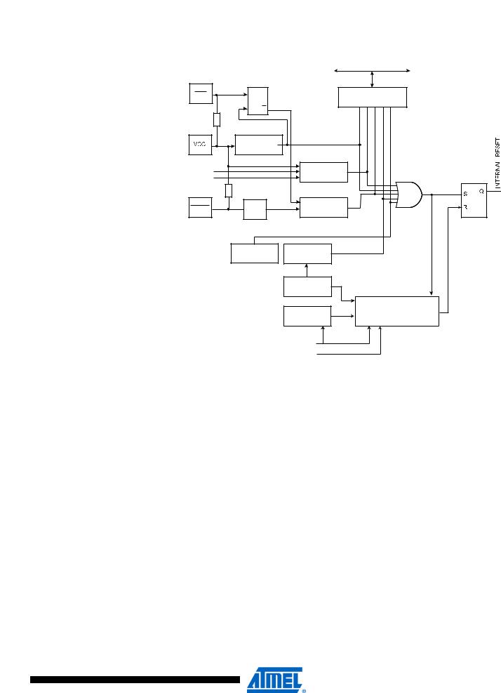
Figure 22. |
Reset Logic |
|
|
|
|
|
|
|
|
|
|
DATA BUS |
|
|
PEN |
D |
Q |
|
MCU Control and Status |
|
|
|
|
|
|
Register (MCUCSR) |
|
|
|
L |
Q |
|
PORF |
BORF EXTRF WDRF JTRF |
|
|
Pull-up Resistor |
|
|||
|
|
|
|
|
||
|
|
Power-On Reset |
|
|
|
|
|
|
Circuit |
|
|
|
|
|
BODEN |
|
|
Brown-Out |
|
|
|
|
|
Reset Circuit |
|
||
BODLEVEL |
|
|
|
|||
|
|
|
|
|
||
|
|
Pull-up Resistor |
|
|
|
|
|
RESET |
SPIKE |
Reset Circuit |
|
|
|
|
FILTER |
|
|
|||
|
|
|
|
|
||
|
|
JTAG Reset |
Watchdog |
|
RESET |
|
|
|
Register |
Timer |
|
COUNTER |
|
|
|
|
|
|||
|
|
|
|
Watchdog |
|
|
|
|
|
|
Oscillator |
|
|
|
|
|
|
Clock |
CK |
Delay Counters |
|
|
|
|
Generator |
|
TIMEOUT |
|
|
|
|
CKSEL[3:0] |
|
|
|
|
|
|
SUT[1:0] |
|
|
Table 19. |
Reset Characteristics |
|
|
|
||
Symbol |
Parameter |
Condition |
Min |
Typ |
Max |
Units |
||||
|
|
|
|
|
|
|
|
|||
|
|
Power-on Reset |
|
|
|
|
|
|||
|
|
Threshold Voltage |
|
|
1.4 |
2.3 |
|
|||
VPOT |
|
(rising) |
|
|
|
|
|
|||
|
|
|
|
|
|
|
|
|
|
|
|
Power-on Reset |
|
|
|
|
V |
||||
|
|
|
|
|
|
|||||
|
|
Threshold Voltage |
|
|
1.3 |
2.3 |
||||
|
|
|
|
|
||||||
|
|
(falling)(1) |
|
|
|
|
|
|||
|
|
|
Pin Threshold |
|
|
|
|
|
||
VRST |
|
RESET |
|
0.2 VCC |
|
0.85 VCC |
|
|||
|
Voltage |
|
|
|
||||||
|
|
Pulse width on |
|
|
|
|
|
|
|
|
tRST |
|
RESET |
|
1.5 |
|
|
µs |
|||
|
Pin |
|
|
|
||||||
VBOT |
|
Brown-out Reset |
BODLEVEL = 1 |
2.4 |
2.6 |
2.9 |
V |
|||
|
Threshold Voltage(2) |
|
|
|
|
|||||
|
BODLEVEL = 0 |
3.7 |
4.0 |
4.5 |
||||||
|
|
|
|
|
|
|
||||
|
|
|
|
|
|
|
|
|||
|
|
Minimum low voltage |
BODLEVEL = 1 |
|
2 |
|
|
|||
tBOD |
|
period for Brown-out |
|
|
|
|
µs |
|||
|
BODLEVEL = 0 |
|
2 |
|
||||||
|
|
Detection |
|
|
|
|||||
|
|
|
|
|
|
|
|
|||
VHYST |
|
Brown-out Detector |
|
|
100 |
|
mV |
|||
|
hysteresis |
|
|
|
||||||
|
|
|
|
|
|
|
||||
|
|
|
|
|
|
|
|
|
|
|
Notes: 1. The Power-on Reset will not work unless the supply voltage has been below VPOT (falling)
50
2467X–AVR–06/11