


 ATmega128
Figure 44. Timer/Counter Timing Diagram, Clear Timer on Compare Match Mode, with Prescaler (fclk_I/O/8)
clkI/O |
|
|
|
|
|
|
|
|
|
|
|
|
|
|
|
|
|
|
|
|
|
|
|
|
|
|
|
|
|
|
|
|
|
|
|
|
|
|
|
|
|
|
|
|
|
|
|
|
|
|
|
|
|
|
|
|
|
|
|
|
|
|
|
|
clkTn |
|
|
|
|
|
|
|
|
|
|
|
|
|
|
|
|
|
|
|
|
|
|
|
|
|
|
|
|
|
|
|
|
|
|
|
|
|
|
|
|
|
|
|
|
|
|
|
|
|
|
|
|
|
|
|
|
|
|
|
|
|
|
|
|
|
|
|
|
|
|
|
|
|
|
|
|
|
|
|
|
|
|
|
|
|
|
|
|
|
|
|
|
|
|
|
|
|
|
|
|
|
|
|
|
|
|
|
|
|
|
|
|
|
|
|
|
|
|
|
|
|
|
|
|
|
|
|
|
|
|
|
|
|
|
|
|
|
|
|
|
|
|
|
|
|
|
|
|
|
|
|
|
|
|
|
|
|
|
|
|
|
|
|
|
|
|
|
|
|
|
|
|
|
|
|
|
|
|
|
|
|
|
|
|
|
|
|
|
|
|
|
|
|
|
(clkI/O/8) |
|
|
|
|
|
|
|
|
|
|
|
|
|
|
|
|
|
|
|
|
|
|
|
|
|
|
|
|
|
|
|
|
|
|
|
|
|
|
|
|
|
|
|
|
|
|
|
|
|
|
|
|
|
|
|
|
|
|
|
|
|
|
|
|
TCNTn |
|
|
|
|
|
|
|
|
|
|
|
|
|
|
|
|
|
|
|
|
|
|
|
|
|
|
|
|
|
|
|
|
|
|
|
|
|
|
|
|
|
|
|
|
|
|
|
|
|
|
|
|
|
|
|
|
|
|
|
|
|
|
|
|
|
|
|
|
|
|
|
|
TOP - 1 |
|
|
|
|
|
|
|
|
|
|
|
TOP |
|
|
|
|
|
|
|
|
|
|
BOTTOM |
|
|
|
|
|
|
BOTTOM + 1 |
|
|||||||||||||||||||||||||
(CTC) |
|
|
|
|
|
|
|
|
|
|
|
|
|
|
|
|
|
|
|
|
|
|
|
|
|
|
|
|
|
|
|
|
|
|
|
|
||||||||||||||||||||||||||||
|
|
|
|
|
|
|
|
|
|
|
|
|
|
|
|
|
|
|
|
|
|
|
|
|
|
|
|
|
|
|
|
|
|
|
|
|
|
|
|
|
|
|
|
|
|
|
|
|
|
|
|
|
|
|
|
|
|
|
|
|
|
|
|
|
OCRn |
|
|
|
|
|
|
|
|
|
|
|
|
|
|
|
|
|
|
|
|
|
|
|
|
|
|
|
|
|
|
|
|
|
|
|
|
|
|
|
|
|
|
|
|
|
|
|
|
|
|
|
|
|
|
|
|
|
|
|
|
|
|
|
|
|
|
|
|
|
|
|
|
|
|
|
|
|
|
|
|
|
|
|
|
|
|
|
|
|
|
|
|
|
|
|
TOP |
|
|
|
|
|
|
|
|
|
|
|
|
|
|
|
|
|
||||||||||||||||
|
|
|
|
|
|
|
|
|
|
|
|
|
|
|
|
|
|
|
|
|
|
|
|
|
|
|
|
|
|
|
|
|
|
|
|
|
|
|
|
|
|
|
|
|
|
|
|
|
|
|
|
|
|
|
|
|
|
|
|
|
|
|
|
|
OCFn
8-bit Timer/Counter Register Description
Timer/Counter Control
Register – TCCR0
Bit |
7 |
6 |
5 |
4 |
3 |
2 |
1 |
0 |
|
|
FOC0 |
WGM00 |
COM01 |
COM00 |
WGM01 |
CS02 |
CS01 |
CS00 |
TCCR0 |
|
|
|
|
|
|
|
|
|
|
Read/Write |
W |
R/W |
R/W |
R/W |
R/W |
R/W |
R/W |
R/W |
|
Initial Value |
0 |
0 |
0 |
0 |
0 |
0 |
0 |
0 |
|
• Bit 7 – FOC0: Force Output Compare
The FOC0 bit is only active when the WGM bits specify a non-PWM mode. However, for ensuring compatibility with future devices, this bit must be set to zero when TCCR0 is written when operating in PWM mode. When writing a logical one to the FOC0 bit, an immediate compare match is forced on the waveform generation unit. The OC0 output is changed according to its COM01:0 bits setting. Note that the FOC0 bit is implemented as a strobe. Therefore it is the value present in the COM01:0 bits that determines the effect of the forced compare.
A FOC0 strobe will not generate any interrupt, nor will it clear the timer in CTC mode using OCR0 as TOP.
The FOC0 bit is always read as zero.
• Bit 6, 3 – WGM01:0: Waveform Generation Mode
These bits control the counting sequence of the counter, the source for the maximum (TOP) counter value, and what type of waveform generation to be used. Modes of operation supported by the Timer/Counter unit are: Normal mode, Clear Timer on Compare match (CTC) mode, and two types of Pulse Width Modulation (PWM) modes. See Table 52 and “Modes of Operation” on page 97.
103
2467X–AVR–06/11

 ATmega128
Table 52. Waveform Generation Mode Bit Description
|
WGM01(1) |
WGM00(1) |
Timer/Counter |
|
Update of |
TOV0 Flag |
Mode |
(CTC0) |
(PWM0) |
Mode of Operation |
TOP |
OCR0 at |
Set on |
|
|
|
|
|
|
|
0 |
0 |
0 |
Normal |
0xFF |
Immediate |
MAX |
|
|
|
|
|
|
|
1 |
0 |
1 |
PWM, Phase |
0xFF |
TOP |
BOTTOM |
|
|
|
Correct |
|
|
|
|
|
|
|
|
|
|
2 |
1 |
0 |
CTC |
OCR0 |
Immediate |
MAX |
|
|
|
|
|
|
|
3 |
1 |
1 |
Fast PWM |
0xFF |
BOTTOM |
MAX |
|
|
|
|
|
|
|
Note: 1. The CTC0 and PWM0 bit definition names are now obsolete. Use the WGM01:0 definitions. However, the functionality and location of these bits are compatible with previous versions of the timer.
• Bit 5:4 – COM01:0: Compare Match Output Mode
These bits control the output compare pin (OC0) behavior. If one or both of the COM01:0 bits are set, the OC0 output overrides the normal port functionality of the I/O pin it is connected to. However, note that the Data Direction Register (DDR) bit corresponding to OC0 pin must be set in order to enable the output driver.
When OC0 is connected to the pin, the function of the COM01:0 bits depends on the WGM01:0 bit setting. Table 53 shows the COM01:0 bit functionality when the WGM01:0 bits are set to a normal or CTC mode (non-PWM).
Table 53. Compare Output Mode, non-PWM Mode
COM01 |
COM00 |
Description |
|
|
|
0 |
0 |
Normal port operation, OC0 disconnected. |
|
|
|
0 |
1 |
Toggle OC0 on compare match |
|
|
|
1 |
0 |
Clear OC0 on compare match |
|
|
|
1 |
1 |
Set OC0 on compare match |
|
|
|
Table 54 shows the COM01:0 bit functionality when the WGM01:0 bits are set to fast PWM mode.
Table 54. Compare Output Mode, Fast PWM Mode(1)
COM01 |
COM00 |
Description |
|
|
|
0 |
0 |
Normal port operation, OC0 disconnected. |
|
|
|
0 |
1 |
Reserved |
|
|
|
1 |
0 |
Clear OC0 on compare match, set OC0 at BOTTOM, |
|
|
(non-inverting mode) |
|
|
|
1 |
1 |
Set OC0 on compare match, clear OC0 at BOTTOM, |
|
|
(inverting mode) |
|
|
|
Note: 1. A special case occurs when OCR0 equals TOP and COM01 is set. In this case, the compare match is ignored, but the set or clear is done at BOTTOM. See “Fast PWM Mode” on page 98 for more details.
Table 55 shows the COM01:0 bit functionality when the WGM01:0 bits are set to phase correct PWM mode.
104
2467X–AVR–06/11

Timer/Counter
Register – TCNT0
Output Compare
Register – OCR0
|
|
ATmega128 |
|
Table 55. Compare Output Mode, Phase Correct PWM Mode(1) |
|||
COM01 |
COM00 |
Description |
|
|
|
|
|
0 |
0 |
Normal port operation, OC0 disconnected. |
|
|
|
|
|
0 |
1 |
Reserved |
|
|
|
|
|
1 |
0 |
Clear OC0 on compare match when up-counting. Set OC0 on compare |
|
|
|
match when downcounting. |
|
|
|
|
|
1 |
1 |
Set OC0 on compare match when up-counting. Clear OC0 on compare |
|
|
|
match when downcounting. |
|
|
|
|
|
Note: 1. A special case occurs when OCR0 equals TOP and COM01 is set. In this case, the compare match is ignored, but the set or clear is done at TOP. See “Phase Correct PWM Mode” on page 100 for more details.
• Bit 2:0 – CS02:0: Clock Select
The three clock select bits select the clock source to be used by the Timer/Counter, see Table 56.
Table 56. Clock Select Bit Description
CS02 |
|
CS01 |
CS00 |
|
Description |
|
|
|
|
|
|
|
|
|
|
|
|
|
|
||||
0 |
0 |
0 |
|
No clock source (Timer/Counter stopped) |
|
|
|||||
|
|
|
|
|
|
|
|
|
|
||
0 |
0 |
1 |
|
clkT0S/(No prescaling) |
|
|
|
|
|||
0 |
1 |
0 |
|
clkT0S/8 (From prescaler) |
|
|
|
||||
0 |
1 |
1 |
|
clkT0S/32 (From prescaler) |
|
|
|
||||
1 |
0 |
0 |
|
clkT0S/64 (From prescaler) |
|
|
|
||||
1 |
0 |
1 |
|
clkT0S/128 (From prescaler) |
|
|
|
||||
1 |
1 |
0 |
|
clkT0S/256 (From prescaler) |
|
|
|
||||
1 |
1 |
1 |
|
clkT0S/1024 (From prescaler) |
|
|
|
||||
Bit |
7 |
6 |
5 |
4 |
3 |
2 |
1 |
0 |
|
||
|
|
|
|
|
|
|
|
|
|
|
|
|
|
|
|
|
|
TCNT0[7:0] |
|
|
|
TCNT0 |
|
|
|
|
|
|
|
|
|
|
|
|
|
Read/Write |
|
R/W |
R/W |
R/W |
R/W |
R/W |
R/W |
R/W |
R/W |
||
Initial Value |
0 |
0 |
0 |
0 |
0 |
0 |
0 |
0 |
|
||
The Timer/Counter Register gives direct access, both for read and write operations, to the Timer/Counter unit 8-bit counter. Writing to the TCNT0 Register blocks (removes) the compare match on the following timer clock. Modifying the counter (TCNT0) while the counter is running, introduces a risk of missing a compare match between TCNT0 and the OCR0 Register.
Bit |
7 |
6 |
5 |
4 |
3 |
2 |
1 |
0 |
|
|
|
|
|
OCR0[7:0] |
|
|
|
OCR0 |
|
|
|
|
|
|
|
|
|
|
|
Read/Write |
R/W |
R/W |
R/W |
R/W |
R/W |
R/W |
R/W |
R/W |
|
Initial Value |
0 |
0 |
0 |
0 |
0 |
0 |
0 |
0 |
|
The Output Compare Register contains an 8-bit value that is continuously compared with the counter value (TCNT0). A match can be used to generate an output compare interrupt, or to generate a waveform output on the OC0 pin.
105
2467X–AVR–06/11

 ATmega128
Asynchronous
Operation of the
Timer/Counter
Asynchronous Status
Register – ASSR
Asynchronous
Operation of
Timer/Counter0
Bit |
7 |
6 |
5 |
4 |
3 |
2 |
1 |
0 |
|
|
– |
– |
– |
– |
AS0 |
TCN0UB |
OCR0UB |
TCR0UB |
ASSR |
Read/Write |
R |
R |
R |
R |
R/W |
R |
R |
R |
|
Initial Value |
0 |
0 |
0 |
0 |
0 |
0 |
0 |
0 |
|
• Bit 3 – AS0: Asynchronous Timer/Counter0
When AS0 is written to zero, Timer/Counter0 is clocked from the I/O clock, clkI/O. When AS0 is written to one, Timer/Counter is clocked from a crystal Oscillator connected to the Timer Oscillator 1 (TOSC1) pin. When the value of AS0 is changed, the contents of TCNT0, OCR0, and TCCR0 might be corrupted.
• Bit 2 – TCN0UB: Timer/Counter0 Update Busy
When Timer/Counter0 operates asynchronously and TCNT0 is written, this bit becomes set. When TCNT0 has been updated from the temporary storage register, this bit is cleared by hardware. A logical zero in this bit indicates that TCNT0 is ready to be updated with a new value.
• Bit 1 – OCR0UB: Output Compare Register0 Update Busy
When Timer/Counter0 operates asynchronously and OCR0 is written, this bit becomes set. When OCR0 has been updated from the temporary storage register, this bit is cleared by hardware. A logical zero in this bit indicates that OCR0 is ready to be updated with a new value.
• Bit 0 – TCR0UB: Timer/Counter Control Register0 Update Busy
When Timer/Counter0 operates asynchronously and TCCR0 is written, this bit becomes set. When TCCR0 has been updated from the temporary storage register, this bit is cleared by hardware. A logical zero in this bit indicates that TCCR0 is ready to be updated with a new value.
If a write is performed to any of the three Timer/Counter0 Registers while its update busy flag is set, the updated value might get corrupted and cause an unintentional interrupt to occur.
The mechanisms for reading TCNT0, OCR0, and TCCR0 are different. When reading TCNT0, the actual timer value is read. When reading OCR0 or TCCR0, the value in the temporary storage register is read.
When Timer/Counter0 operates asynchronously, some considerations must be taken.
•Warning: When switching between asynchronous and synchronous clocking of Timer/Counter0, the Timer Registers TCNT0, OCR0, and TCCR0 might be corrupted. A safe procedure for switching clock source is:
1.Disable the Timer/Counter0 interrupts by clearing OCIE0 and TOIE0.
2.Select clock source by setting AS0 as appropriate.
3.Write new values to TCNT0, OCR0, and TCCR0.
4.To switch to asynchronous operation: Wait for TCN0UB, OCR0UB, and TCR0UB.
5.Clear the Timer/Counter0 interrupt flags.
6.Enable interrupts, if needed.
•The Oscillator is optimized for use with a 32.768 kHz watch crystal. Applying an external clock to the TOSC1 pin may result in incorrect Timer/Counter0 operation. The CPU main clock frequency must be more than four times the Oscillator frequency.
106
2467X–AVR–06/11

 ATmega128
•When writing to one of the registers TCNT0, OCR0, or TCCR0, the value is transferred to a temporary register, and latched after two positive edges on TOSC1. The user should not write a new value before the contents of the Temporary Register have been transferred to its destination. Each of the three mentioned registers have their individual temporary register, which means that e.g., writing to TCNT0 does not disturb an OCR0 write in progress. To detect that a transfer to the destination register has taken place, the Asynchronous Status Register – ASSR has been implemented.
•When entering Power-save or Extended Standby mode after having written to TCNT0, OCR0, or TCCR0, the user must wait until the written register has been updated if Timer/Counter0 is used to wake up the device. Otherwise, the MCU will enter sleep mode before the changes are effective. This is particularly important if the Output Compare0 interrupt is used to wake up the device, since the output compare function is disabled during writing to OCR0 or TCNT0. If the write cycle is not finished, and the MCU enters sleep mode before the OCR0UB bit returns to zero, the device will never receive a compare match interrupt, and the MCU will not wake up.
•If Timer/Counter0 is used to wake the device up from Power-save or Extended Standby mode, precautions must be taken if the user wants to re-enter one of these modes: The interrupt logic needs one TOSC1 cycle to be reset. If the time between wake-up and reentering sleep mode is less than one TOSC1 cycle, the interrupt will not occur, and the device will fail to wake up. If the user is in doubt whether the time before re-entering Powersave or Extended Standby mode is sufficient, the following algorithm can be used to ensure that one TOSC1 cycle has elapsed:
1.Write a value to TCCR0, TCNT0, or OCR0.
2.Wait until the corresponding Update Busy flag in ASSR returns to zero.
3.Enter Power-save or Extended Standby mode.
•When the asynchronous operation is selected, the 32.768kHz Oscillator for Timer/Counter0 is always running, except in Power-down and Standby modes. After a Power-up Reset or wake-up from Power-down or Standby mode, the user should be aware of the fact that this Oscillator might take as long as one second to stabilize. The user is advised to wait for at least one second before using Timer/Counter0 after power-up or wake-up from Power-down or Standby mode. The contents of all Timer/Counter0 Registers must be considered lost after a wake-up from Power-down or Standby mode due to unstable clock signal upon startup, no matter whether the Oscillator is in use or a clock signal is applied to the TOSC1 pin.
•Description of wake up from Power-save or Extended Standby mode when the timer is clocked asynchronously: When the interrupt condition is met, the wake up process is started on the following cycle of the timer clock, that is, the timer is always advanced by at least one before the processor can read the counter value. After wake-up, the MCU is halted for four cycles, it executes the interrupt routine, and resumes execution from the instruction following SLEEP.
•Reading of the TCNT0 Register shortly after wake-up from Power-save may give an incorrect result. Since TCNT0 is clocked on the asynchronous TOSC clock, reading TCNT0 must be done through a register synchronized to the internal I/O clock domain. Synchronization takes place for every rising TOSC1 edge. When waking up from Power-
save mode, and the I/O clock (clkI/O) again becomes active, TCNT0 will read as the previous value (before entering sleep) until the next rising TOSC1 edge. The phase of the TOSC clock after waking up from Power-save mode is essentially unpredictable, as it depends on the wake-up time. The recommended procedure for reading TCNT0 is thus as follows:
1.Write any value to either of the registers OCR0 or TCCR0.
2.Wait for the corresponding Update Busy Flag to be cleared.
3.Read TCNT0.
107
2467X–AVR–06/11

 ATmega128
Timer/Counter
Interrupt Mask
Register – TIMSK
•During asynchronous operation, the synchronization of the interrupt flags for the asynchronous timer takes three processor cycles plus one timer cycle. The timer is therefore advanced by at least one before the processor can read the timer value causing the setting of the interrupt flag. The output compare pin is changed on the timer clock and is not synchronized to the processor clock.
Bit |
7 |
6 |
5 |
4 |
3 |
2 |
1 |
0 |
|
|
OCIE2 |
TOIE2 |
TICIE1 |
OCIE1A |
OCIE1B |
TOIE1 |
OCIE0 |
TOIE0 |
TIMSK |
Read/Write |
R/W |
R/W |
R/W |
R/W |
R/W |
R/W |
R/W |
R/W |
|
Initial Value |
0 |
0 |
0 |
0 |
0 |
0 |
0 |
0 |
|
• Bit 1 – OCIE0: Timer/Counter0 Output Compare Match Interrupt Enable
When the OCIE0 bit is written to one, and the I-bit in the Status Register is set (one), the Timer/Counter0 Compare Match interrupt is enabled. The corresponding interrupt is executed if a compare match in Timer/Counter0 occurs, i.e., when the OCF0 bit is set in the Timer/Counter Interrupt Flag Register – TIFR.
• Bit 0 – TOIE0: Timer/Counter0 Overflow Interrupt Enable
When the TOIE0 bit is written to one, and the I-bit in the Status Register is set (one), the Timer/Counter0 Overflow interrupt is enabled. The corresponding interrupt is executed if an overflow in Timer/Counter0 occurs, i.e., when the TOV0 bit is set in the Timer/Counter Interrupt Flag Register – TIFR.
Timer/Counter
Interrupt Flag Register
– TIFR
Bit |
7 |
6 |
5 |
4 |
3 |
2 |
1 |
0 |
|
|
OCF2 |
TOV2 |
ICF1 |
OCF1A |
OCF1B |
TOV1 |
OCF0 |
TOV0 |
TIFR |
Read/Write |
R/W |
R/W |
R/W |
R/W |
R/W |
R/W |
R/W |
R/W |
|
Initial Value |
0 |
0 |
0 |
0 |
0 |
0 |
0 |
0 |
|
• Bit 1 – OCF0: Output Compare Flag 0
The OCF0 bit is set (one) when a compare match occurs between the Timer/Counter0 and the data in OCR0 – Output Compare Register0. OCF0 is cleared by hardware when executing the corresponding interrupt handling vector. Alternatively, OCF0 is cleared by writing a logic one to the flag. When the I-bit in SREG, OCIE0 (Timer/Counter0 Compare Match Interrupt Enable), and OCF0 are set (one), the Timer/Counter0 Compare Match Interrupt is executed.
• Bit 0 – TOV0: Timer/Counter0 Overflow Flag
The bit TOV0 is set (one) when an overflow occurs in Timer/Counter0. TOV0 is cleared by hardware when executing the corresponding interrupt handling vector. Alternatively, TOV0 is cleared by writing a logic one to the flag. When the SREG I-bit, TOIE0 (Timer/Counter0 Overflow Interrupt Enable), and TOV0 are set (one), the Timer/Counter0 Overflow Interrupt is executed. In PWM mode, this bit is set when Timer/Counter0 changes counting direction at $00.
108
2467X–AVR–06/11
 ATmega128
Timer/Counter
Prescaler
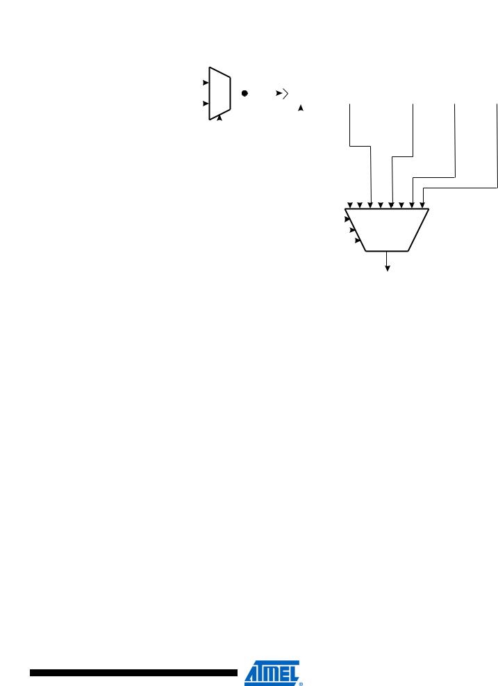
Figure 45. Prescaler for Timer/Counter0
clkI/O |
|
|
|
|
clkT0S |
|
|
|
|
|
|
|
|
|
|
|
|
|
|
||
|
|
|
|
|
|
|
|
|
|
|
10-BIT T/C PRESCALER |
|
|
||||||||
|
|
|
|
|
|
|
|
|
|
|
|
|
|
|
|||||||
TOSC1 |
|
|
|
|
|
|
Clear |
|
|
|
|
||||||||||
|
|
|
|
|
|
|
|
|
|
|
|
|
|
|
|||||||
|
|
|
|
|
|
|
|
/8 |
|
|
|
|
|
|
/32 |
/64 |
/128 |
/256 |
/1024 |
||
|
|
|
|
|
|
|
|
|
|
||||||||||||
|
|
|
|
|
|
|
|
|
|
|
|
|
|||||||||
|
|
|
|
|
|
|
|
|
|
T0S |
|
|
|
|
T0S |
T0S |
|||||
|
|
|
|
|
|
|
|
|
|
|
|
|
|
T0S |
T0S |
T0S |
|||||
AS0 |
|
|
|
|
|
|
|
|
clk |
|
|
|
|
clk |
clk |
clk |
clk |
clk |
|||
|
|
|
|
|
|
|
|
|
|
|
|
|
|
|
|
|
|||||
|
|
|
|
|
|
|
|
|
|
|
|
|
|
|
|
|
|
|
|
||
PSR0 |
|
|
|
|
|
|
|
|
|
|
|
|
|
|
|
|
|
|
|
|
|
|
|
|
|
|
|
|
|
|
|
|
|
|
|
|
|
|
|
|
|
|
|
|
|
|
|
|
|
|
|
|
|
|
|
|
|
|
|
|
|
|
|
|
|
|
|
|
|
|
|
|
|
|
|
|
|
|
|
|
|
|
|
|
|
|
|
|
0 |
|
|
|
|
|
|
|
|
|
|||||||||||
|
|
|
|
|
|
|
|
|
|
|
|||||||||||
CS00 |
|
|
|
|
|
|
|
|
|
|
|
|
|
|
|
|
|
|
|
|
|
|
|
|
|
|
|
|
|
|
|
|
|
|
|
|
|
|
|
|
|
||
|
|
|
|
|
|
|
|
|
|
|
|
|
|
|
|
|
|
|
|
||
CS01 |
|
|
|
|
|
|
|
|
|
|
|
|
|
|
|
|
|
|
|
|
|
|
|
|
|
|
|
|
|
|
|
|
|
|
|
|
|
|
|
|
|
||
CS02 |
|
|
|
|
|
|
|
|
|
|
|
|
|
|
|
|
|
|
|
|
|
|
|
|
|
|
|
|
|
|
|
|
|
|
|
|
|
|
|
|
|
||
Special Function IO
Register – SFIOR
TIMER/COUNTER0 CLOCK SOURCE clkT0
The clock source for Timer/Counter0 is named clkT0. clkT0 is by default connected to the main system clock clkI/O. By setting the AS0 bit in ASSR, Timer/Counter0 is asynchronously clocked from the TOSC1 pin. This enables use of Timer/Counter0 as a Real Time Counter (RTC). When AS0 is set, pins TOSC1 and TOSC2 are disconnected from Port C. A crystal can then be connected between the TOSC1 and TOSC2 pins to serve as an independent clock source for Timer/Counter0. The Oscillator is optimized for use with a 32.768kHz crystal. Applying an external clock source to TOSC1 is not recommended.
For Timer/Counter0, the possible prescaled selections are: clkT0S/8, clkT0S/32, clkT0S/64, clkT0S/128, clkT0S/256, and clkT0S/1024. Additionally, clkT0S as well as 0 (stop) may be selected. Setting the PSR0 bit in SFIOR resets the prescaler. This allows the user to operate with a predictable prescaler.
Bit |
7 |
6 |
5 |
4 |
3 |
2 |
1 |
0 |
|
|
TSM |
– |
– |
– |
ACME |
PUD |
PSR0 |
PSR321 |
SFIOR |
Read/Write |
R/W |
R |
R |
R |
R/W |
R/W |
R/W |
R/W |
|
Initial Value |
0 |
0 |
0 |
0 |
0 |
0 |
0 |
0 |
|
• Bit 7 – TSM: Timer/Counter Synchronization Mode
Writing the TSM bit to one activates the Timer/Counter Synchronization mode. In this mode, the value that is written to the PSR0 and PSR321 bits is kept, hence keeping the corresponding prescaler reset signals asserted. This ensures that the corresponding Timer/Counters are halted and can be configured to the same value without the risk of one of them advancing during configuration. When the TSM bit is written to zero, the PSR0 and PSR321 bits are cleared by hardware, and the Timer/Counters start counting simultaneously.
109
2467X–AVR–06/11

 ATmega128
• Bit 1 – PSR0: Prescaler Reset Timer/Counter0
When this bit is one, the Timer/Counter0 prescaler will be reset. This bit is normally cleared immediately by hardware. If this bit is written when Timer/Counter0 is operating in asynchronous mode, the bit will remain one until the prescaler has been reset. The bit will not be cleared by hardware if the TSM bit is set.
110
2467X–AVR–06/11