

 ATmega128
|
2. VBOT may be below nominal minimum operating voltage for some devices. For devices where |
||||||||||||||||||||||
|
|
this is the case, the device is tested down to VCC = VBOT during the production test. This guar- |
|||||||||||||||||||||
|
|
antees that a Brown-out Reset will occur before VCC drops to a voltage where correct |
|||||||||||||||||||||
|
|
operation of the microcontroller is no longer guaranteed. The test is performed using |
|||||||||||||||||||||
|
|
BODLEVEL=1for ATmega128L and BODLEVEL=0 for ATmega128. BODLEVEL=1 is not |
|||||||||||||||||||||
|
|
applicable forATmega128 |
|
|
|
|
|
|
|
|
|
|
|
|
|
|
|||||||
Power-on Reset |
A Power-on Reset (POR) pulse is generated by an On-chip detection circuit. The detection level |
||||||||||||||||||||||
|
is defined in Table 19. The POR is activated whenever VCC is below the detection level. The |
||||||||||||||||||||||
|
POR circuit can be used to trigger the Start-up Reset, as well as to detect a failure in supply |
||||||||||||||||||||||
|
voltage. |
|
|
|
|
|
|
|
|
|
|
|
|
|
|
||||||||
|
A Power-on Reset (POR) circuit ensures that the device is reset from Power-on. Reaching the |
||||||||||||||||||||||
|
Power-on Reset threshold voltage invokes the delay counter, which determines how long the |
||||||||||||||||||||||
|
device is kept in RESET after VCC rise. The RESET signal is activated again, without any delay, |
||||||||||||||||||||||
|
when VCC decreases below the detection level. |
||||||||||||||||||||||
|
Figure 23. MCU Start-up, |
|
|
|
Tied to VCC. |
||||||||||||||||||
|
RESET |
||||||||||||||||||||||
|
|
|
|
|
|
|
|
VPOT |
|
|
|
|
|
|
|
|
|
|
|
|
|
|
|
|
|
VCC |
|
|
|
|
|
|
|
|
|
|
|
|
|
|
|||||||
|
|
|
|
|
|
|
|
VRST |
|
|
|
|
|
|
|
|
|
|
|
|
|
|
|
|
|
|
|
|
|
|
|
|
|
|
|
|
|
|
|
|
|
|
|
|
|
||
|
|
RESET |
|
|
|
|
|
|
|
|
|
|
|
|
|
|
|||||||
|
TIME-OUT |
|
|
|
|
tTOUT |
|
|
|
|
|
|
|
|
|
|
|||||||
|
|
|
|
|
|
|
|
|
|
|
|
|
|
||||||||||
|
|
|
|
|
|
|
|
|
|
|
|
|
|
|
|
|
|||||||
|
|
|
|
|
|
|
|
|
|
|
|
|
|
|
|
|
|
|
|
|
|||
|
INTERNAL |
|
|
|
|
|
|
|
|
|
|
|
|
|
|
|
|
|
|
||||
|
RESET |
|
|
|
|
|
|
|
|
|
|
|
|
|
|
|
|
|
|
||||
|
Figure 24. MCU Start-up, |
|
|
|
Extended Externally |
||||||||||||||||||
|
RESET |
||||||||||||||||||||||
|
|
|
|
|
|
|
|
VPOT |
|
|
|
|
|
|
|
|
|
|
|
|
|
|
|
|
|
VCC |
|
|
|
|
|
|
|
|
|
|
|
|
|
|
|||||||
|
|
|
|
|
|
|
|
|
|
|
|
|
|
|
VRST |
||||||||
|
|
RESET |
|
|
|
|
|||||||||||||||||
|
|
|
|
|
|
|
|
|
|
|
|
|
|
|
|
||||||||
|
TIME-OUT |
|
|
|
|
|
|
|
tTOUT |
|
|
|
|
||||||||||
|
|
|
|
|
|
|
|
|
|
||||||||||||||
|
|
|
|
|
|
|
|
|
|
|
|||||||||||||
|
|
|
|
|
|
|
|
|
|
|
|
|
|
|
|||||||||
|
|
|
|
|
|
|
|
|
|
|
|
|
|
|
|
||||||||
|
INTERNAL |
|
|
|
|
|
|
|
|
|
|
|
|
|
|
|
|
|
|
||||
External Reset |
RESET |
|
|
|
|
|
|
|
|
|
|
|
|
|
|
|
|
||||||
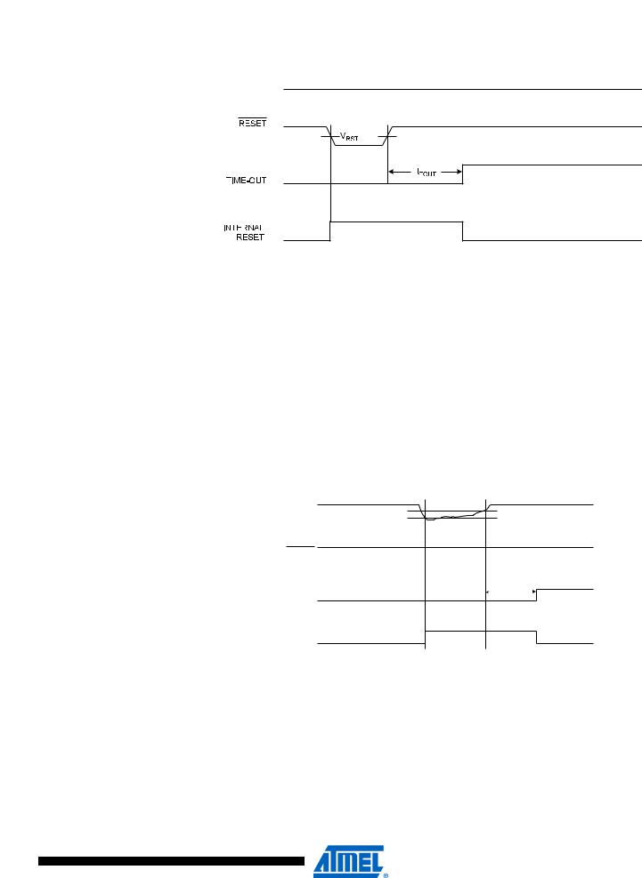
An External Reset is generated by a low level on the |
|
|
|
|
pin. Reset pulses longer than the |
||||||||||||||||||
RESET |
|||||||||||||||||||||||
|
minimum pulse width (see Table 19) will generate a reset, even if the clock is not running. |
||||||||||||||||||||||
|
Shorter pulses are not guaranteed to generate a reset. When the applied signal reaches the |
||||||||||||||||||||||
Reset Threshold Voltage – VRST on its positive edge, the delay counter starts the MCU after the Time-out period tTOUT has expired.
51
2467X–AVR–06/11
 ATmega128
Figure 25. External Reset During Operation
 CC
CC
Brown-out Detection ATmega128 has an On-chip Brown-out Detection (BOD) circuit for monitoring the VCC level during operation by comparing it to a fixed trigger level. The trigger level for the BOD can be selected by the fuse BODLEVEL to be 2.7V (BODLEVEL unprogrammed), or 4.0V (BODLEVEL programmed). The trigger level has a hysteresis to ensure spike free Brown-out Detection. The
hysteresis on the detection level should be interpreted as VBOT+ = VBOT + VHYST/2 and VBOT- =
VBOT - VHYST/2.
The BOD circuit can be enabled/disabled by the fuse BODEN. When the BOD is enabled (BODEN programmed), and VCC decreases to a value below the trigger level (VBOT- in Figure 26), the Brown-out Reset is immediately activated. When VCC increases above the trigger level
(VBOT+ in Figure 26), the delay counter starts the MCU after the time-out period tTOUT has expired.
The BOD circuit will only detect a drop in VCC if the voltage stays below the trigger level for longer than tBOD given in Table 19.
Figure 26. Brown-out Reset During Operation
VCC |
VBOT+ |
|
VBOT- |
RESET |
|
TIME-OUT |
tTOUT |
INTERNAL |
|
RESET |
|
52
2467X–AVR–06/11
 ATmega128
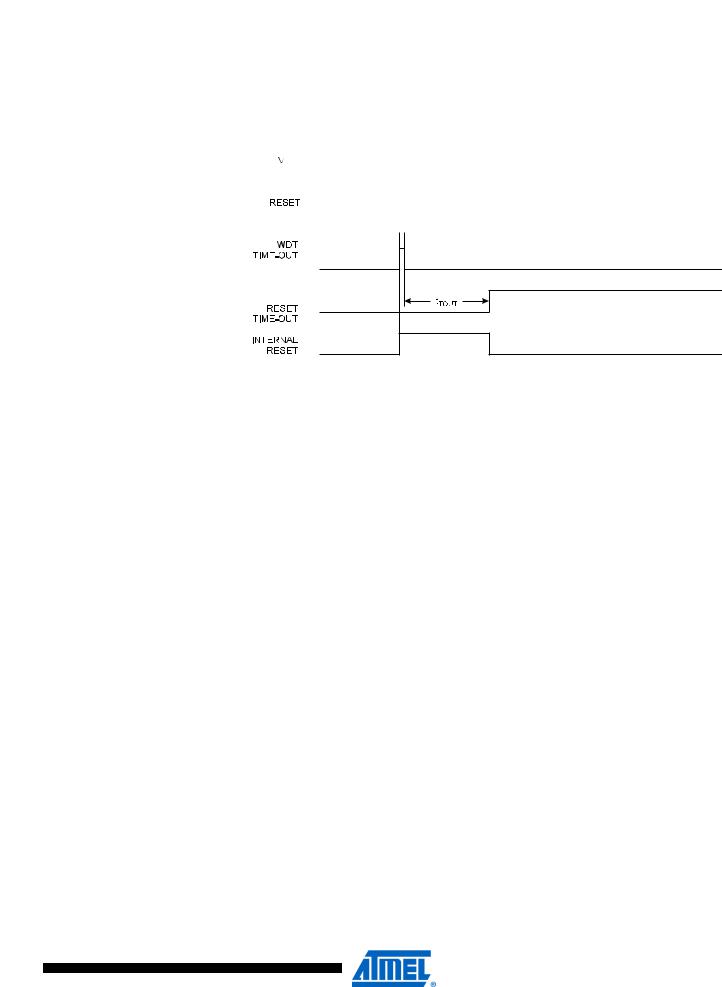
Watchdog Reset |
When the Watchdog times out, it will generate a short reset pulse of 1 CK cycle duration. On the |
||||
|
falling edge of this pulse, the delay timer starts counting the Time-out period tTOUT. Refer to page |
||||
|
54 for details on operation of the Watchdog Timer. |
||||
|
Figure 27. Watchdog Reset During Operation |
||||
|
|
CC |
|
|
|
|
|
||||
|
|
|
|
|
|
|
|
|
|
|
|


 CK
CK 

MCU Control and |
The MCU Control and Status Register provides information on which reset source caused an |
|||||||||
Status Register – |
MCU reset. |
|
|
|
|
|
|
|
|
|
MCUCSR |
Bit |
7 |
6 |
5 |
4 |
3 |
2 |
1 |
0 |
|
|
|
|||||||||
|
|
|
|
|
|
|
|
|
|
|
|
|
JTD |
– |
– |
JTRF |
WDRF |
BORF |
EXTRF |
PORF |
MCUCSR |
|
Read/Write |
R/W |
R |
R |
R/W |
R/W |
R/W |
R/W |
R/W |
|
|
Initial Value |
0 |
0 |
0 |
|
See Bit Description |
|
|
||
Internal Voltage
Reference
Note that only EXTRF and PORF are available in Atmel® AVR®ATmega103 compatibility mode.
• Bit 4 – JTRF: JTAG Reset Flag
This bit is set if a reset is being caused by a logic one in the JTAG Reset Register selected by the JTAG instruction AVR_RESET. This bit is reset by a Power-on Reset, or by writing a logic zero to the flag.
• Bit 3 – WDRF: Watchdog Reset Flag
This bit is set if a Watchdog Reset occurs. The bit is reset by a Power-on Reset, or by writing a logic zero to the flag.
• Bit 2 – BORF: Brown-out Reset Flag
This bit is set if a Brown-out Reset occurs. The bit is reset by a Power-on Reset, or by writing a logic zero to the flag.
• Bit 1 – EXTRF: External Reset Flag
This bit is set if an External Reset occurs. The bit is reset by a Power-on Reset, or by writing a logic zero to the flag.
• Bit 0 – PORF: Power-On Reset Flag
This bit is set if a Power-on Reset occurs. The bit is reset only by writing a logic zero to the flag.
To make use of the reset flags to identify a reset condition, the user should read and then reset the MCUCSR as early as possible in the program. If the register is cleared before another reset occurs, the source of the reset can be found by examining the reset flags.
ATmega128 features an internal bandgap reference. This reference is used for Brown-out Detection, and it can be used as an input to the Analog Comparator or the ADC. The 2.56V reference to the ADC is generated from the internal bandgap reference.
53
2467X–AVR–06/11