

- •Features
- •Overview
- •Block Diagram
- •Pin Descriptions
- •Port A (PA7..PA0)
- •Port B (PB7..PB0)
- •Port C (PC7..PC0)
- •Port D (PD7..PD0)
- •Port E (PE7..PE0)
- •Port F (PF7..PF0)
- •Port G (PG4..PG0)
- •RESET
- •XTAL1
- •XTAL2
- •AVCC
- •AREF
- •Resources
- •Data Retention
- •Capacitive touch sensing
- •AVR CPU Core
- •Introduction
- •Status Register
- •Stack Pointer
- •I/O Memory
- •Overview
- •Timing
- •Using all Locations of External Memory Smaller than 64 Kbyte
- •Clock Systems and their Distribution
- •CPU Clock – clkCPU
- •I/O Clock – clkI/O
- •Flash Clock – clkFLASH
- •ADC Clock – clkADC
- •Clock Sources
- •Crystal Oscillator
- •External Clock
- •Idle Mode
- •Power-down Mode
- •Power-save Mode
- •Standby Mode
- •Analog Comparator
- •Brown-out Detector
- •Watchdog Timer
- •Port Pins
- •Resetting the AVR
- •Reset Sources
- •Power-on Reset
- •External Reset
- •Watchdog Reset
- •Watchdog Timer
- •Timed Sequences for Changing the Configuration of the Watchdog Timer
- •Safety Level 0
- •Safety Level 1
- •Safety Level 2
- •Interrupts
- •I/O Ports
- •Introduction
- •Configuring the Pin
- •Reading the Pin Value
- •Unconnected pins
- •Alternate Port Functions
- •Register Description for I/O Ports
- •8-bit Timer/Counter0 with PWM and Asynchronous Operation
- •Overview
- •Registers
- •Definitions
- •Counter Unit
- •Normal Mode
- •Fast PWM Mode
- •8-bit Timer/Counter Register Description
- •Overview
- •Registers
- •Definitions
- •Compatibility
- •Counter Unit
- •Input Capture Unit
- •Noise Canceler
- •Force Output Compare
- •Normal Mode
- •Fast PWM Mode
- •16-bit Timer/Counter Register Description
- •Internal Clock Source
- •Prescaler Reset
- •External Clock Source
- •8-bit Timer/Counter2 with PWM
- •Overview
- •Registers
- •Definitions
- •Counter Unit
- •Normal Mode
- •Fast PWM Mode
- •8-bit Timer/Counter Register Description
- •Output Compare Modulator (OCM1C2)
- •Overview
- •Description
- •Timing Example
- •Slave Mode
- •Master Mode
- •Data Modes
- •USART
- •Dual USART
- •Overview
- •AVR USART vs. AVR UART – Compatibility
- •Clock Generation
- •External Clock
- •Frame Formats
- •Parity Bit Calculation
- •Parity Generator
- •Receiver Error Flags
- •Parity Checker
- •Disabling the Receiver
- •Using MPCM
- •Features
- •TWI Terminology
- •Transferring Bits
- •Address Packet Format
- •Data Packet Format
- •Overview of the TWI Module
- •Scl and SDA Pins
- •Bus Interface Unit
- •Address Match Unit
- •Control Unit
- •Using the TWI
- •Master Receiver Mode
- •Slave Receiver Mode
- •Miscellaneous States
- •Analog Comparator
- •Analog to Digital Converter
- •Features
- •Operation
- •Changing Channel or Reference Selection
- •ADC Input Channels
- •Analog Input Circuitry
- •Features
- •Overview
- •TAP Controller
- •PRIVATE0; $8
- •PRIVATE1; $9
- •PRIVATE2; $A
- •PRIVATE3; $B
- •Bibliography
- •Features
- •System Overview
- •Data Registers
- •Bypass Register
- •Reset Register
- •EXTEST; $0
- •IDCODE; $1
- •AVR_RESET; $C
- •BYPASS; $F
- •Scanning the ADC
- •ATmega128 Boundary-scan Order
- •Application Section
- •Programming Time for Flash when Using SPM
- •Simple Assembly Code Example for a Boot Loader
- •Fuse Bits
- •Latching of Fuses
- •Signature Bytes
- •Calibration Byte
- •Signal Names
- •Chip Erase
- •Reading the Flash
- •Reading the EEPROM
- •Data Polling Flash
- •Data Polling EEPROM
- •AVR_RESET ($C)
- •PROG_ENABLE ($4)
- •Data Registers
- •Reset Register
- •Programming Enable Register
- •Programming Command Register
- •Virtual Flash Page Read Register
- •Performing Chip Erase
- •Reading the Flash
- •Reading the EEPROM
- •Electrical Characteristics
- •Absolute Maximum Ratings*
- •DC Characteristics
- •Speed Grades
- •External Clock Drive Waveforms
- •External Clock Drive
- •Two-wire Serial Interface Characteristics
- •ADC Characteristics
- •External Data Memory Timing
- •Idle Supply Current
- •Pin Pull-up
- •Pin Driver Strength
- •Register Summary
- •Instruction Set Summary
- •Ordering Information
- •Packaging Information
- •Errata
- •ATmega128 Rev. F to M

 ATmega128
Analog to Digital Converter
Features
•10-bit Resolution
•0.5LSB Integral Non-linearity
•±2LSB Absolute Accuracy
•13 - 260µs Conversion Time
•Up to 76.9kSPS (Up to 15 kSPS at Maximum Resolution)
•8 Multiplexed Single Ended Input Channels
•7 Differential Input Channels
•2 Differential Input Channels with Optional Gain of 10x and 200x
•Optional Left Adjustment for ADC Result Readout
•0 - VCC ADC Input Voltage Range
•Selectable 2.56V ADC Reference Voltage
•Free Running or Single Conversion Mode
•Interrupt on ADC Conversion Complete
•Sleep Mode Noise Canceler
The Atmel® AVR®ATmega128 features a 10-bit successive approximation ADC. The ADC is connected to an 8-channel Analog Multiplexer which allows 8 single-ended voltage inputs constructed from the pins of Port F. The single-ended voltage inputs refer to 0V (GND).
The device also supports 16 differential voltage input combinations. Two of the differential inputs (ADC1, ADC0 and ADC3, ADC2) are equipped with a programmable gain stage, providing amplification steps of 0 dB (1x), 20dB (10x), or 46dB (200x) on the differential input voltage before the A/D conversion. Seven differential analog input channels share a common negative terminal (ADC1), while any other ADC input can be selected as the positive input terminal. If 1x or 10x gain is used, 8-bit resolution can be expected. If 200x gain is used, 7-bit resolution can be expected.
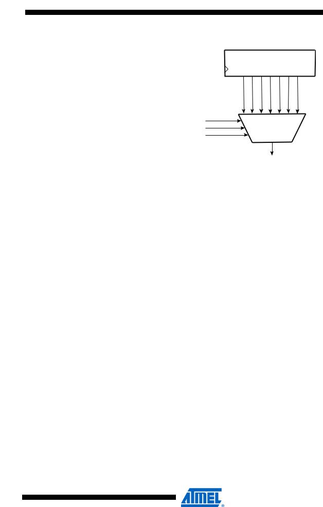
The ADC contains a Sample and Hold circuit which ensures that the input voltage to the ADC is held at a constant level during conversion. A block diagram of the ADC is shown in Figure 108.
The ADC has a separate analog supply voltage pin, AVCC. AVCC must not differ more than ±0.3V from VCC. See the paragraph “ADC Noise Canceler” on page 236 on how to connect this pin.
Internal reference voltages of nominally 2.56V or AVCC are provided On-chip. The voltage reference may be externally decoupled at the AREF pin by a capacitor for better noise performance.
230
2467X–AVR–06/11
ATmega128
Figure 108. Analog to Digital Converter Block Schematic
8-BIT DATA BUS
ADC MULTIPLEXER
SELECT (ADMUX)
REFS1 |
REFS0 |
ADLAR |
MUX4 |
MUX3 |
MUX2 |
MUX1 |
MUX0 |
|
|
|
|
|
|
|
|
|
|
|
|
|
|
|
MUX DECODER |
AVCC |
|
|
|
|
|
CHANNELSELECTION |
GAIN SELECTION |
|
|
|
|
|
|||
|
|
|
|
|
|||
|
|
|
|
|
|
|
|
|
|
|
|
|
|
|
|
INTERNAL 2.56V
REFERENCE
AREF
AGND
BANDGAP
REFERENCE
ADC7
ADC6
POS.
ADC5 INPUT
MUX
ADC4
ADC3

 + ADC2
-
ADC1
ADC0
NEG.
INPUT
MUX
ADC CONVERSION
COMPLETE IRQ
|
|
|
ADIF |
ADIE |
|
|
15 |
|
0 |
|
|
|
|
|
|
|
|||||
|
|
|
|
|||||||
|
ADC CTRL. & STATUS |
|
|
ADC DATA REGISTER |
||||||
|
REGISTER (ADCSRA) |
|
|
(ADCH/ADCL) |
||||||
ADEN |
ADSC |
ADFR |
ADIF |
|
ADPS2 |
ADPS1 |
ADPS0 |
ADC[9:0] |
||
PRESCALER
CONVERSION LOGIC
SAMPLE & HOLD
COMPARATOR
10-BIT DAC |
- |
+
SINGLE ENDED / DIFFERENTIAL SELECTION
ADC MULTIPLEXER
OUTPUT
GAIN
AMPLIFIER
231
2467X–AVR–06/11

Operation
Starting a
Conversion
ATmega128
The ADC converts an analog input voltage to a 10-bit digital value through successive approximation. The minimum value represents GND and the maximum value represents the voltage on the AREF pin minus 1 SB. Optionally, AVCC or an internal 2.56V reference voltage may be connected to the AREF pin by writing to the REFSn bits in the ADMUX Register. The internal voltage reference may thus be decoupled by an external capacitor at the AREF pin to improve noise immunity.
The analog input channel and differential gain are selected by writing to the MUX bits in ADMUX. Any of the ADC input pins, as well as GND and a fixed bandgap voltage reference, can be selected as single ended inputs to the ADC. A selection of ADC input pins can be selected as positive and negative inputs to the differential gain amplifier.
If differential channels are selected, the differential gain stage amplifies the voltage difference between the selected input channel pair by the selected gain factor. This amplified value then becomes the analog input to the ADC. If single ended channels are used, the gain amplifier is bypassed altogether.
The ADC is enabled by setting the ADC Enable bit, ADEN in ADCSRA. Voltage reference and input channel selections will not go into effect until ADEN is set. The ADC does not consume power when ADEN is cleared, so it is recommended to switch off the ADC before entering power saving sleep modes.
The ADC generates a 10-bit result which is presented in the ADC Data Registers, ADCH and ADCL. By default, the result is presented right adjusted, but can optionally be presented left adjusted by setting the ADLAR bit in ADMUX.
If the result is left adjusted and no more than 8-bit precision is required, it is sufficient to read ADCH. Otherwise, ADCL must be read first, then ADCH, to ensure that the content of the data registers belongs to the same conversion. Once ADCL is read, ADC access to data registers is blocked. This means that if ADCL has been read, and a conversion completes before ADCH is read, neither register is updated and the result from the conversion is lost. When ADCH is read, ADC access to the ADCH and ADCL Registers is re-enabled.
The ADC has its own interrupt which can be triggered when a conversion completes. When ADC access to the data registers is prohibited between reading of ADCH and ADCL, the interrupt will trigger even if the result is lost.
A single conversion is started by writing a logical one to the ADC Start Conversion bit, ADSC. This bit stays high as long as the conversion is in progress and will be cleared by hardware when the conversion is completed. If a different data channel is selected while a conversion is in progress, the ADC will finish the current conversion before performing the channel change.
In Free Running mode, the ADC is constantly sampling and updating the ADC Data Register. Free Running mode is selected by writing the ADFR bit in ADCSRA to one. The first conversion must be started by writing a logical one to the ADSC bit in ADCSRA. In this mode the ADC will perform successive conversions independently of whether the ADC Interrupt Flag, ADIF is cleared or not.
232
2467X–AVR–06/11
ATmega128
Prescaling and
Conversion Timing
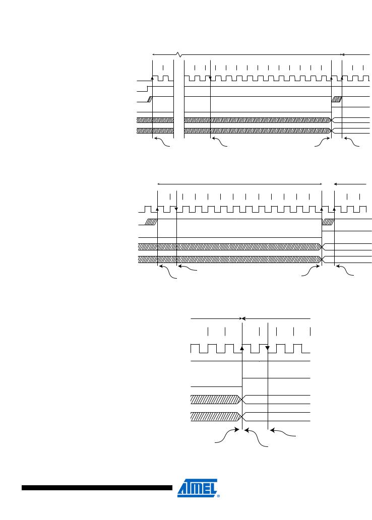
Figure 109. ADC Prescaler
ADEN 
 Reset
Reset
7-BIT ADC PRESCALER
CK 
CK/2 |
CK/4 |
CK/8 |
CK/16 |
CK/32 |
CK/64 |
CK/128 |
ADPS0
ADPS1
ADPS2
ADC CLOCK SOURCE
By default, the successive approximation circuitry requires an input clock frequency between 50kHz and 200kHz to get maximum resolution. If a lower resolution than 10 bits is needed, the input clock frequency to the ADC can be higher than 200kHz to get a higher sample rate.
The ADC module contains a prescaler, which generates an acceptable ADC clock frequency from any CPU frequency above 100kHz. The prescaling is set by the ADPS bits in ADCSRA. The prescaler starts counting from the moment the ADC is switched on by setting the ADEN bit in ADCSRA. The prescaler keeps running for as long as the ADEN bit is set, and is continuously reset when ADEN is low.
When initiating a single ended conversion by setting the ADSC bit in ADCSRA, the conversion starts at the following rising edge of the ADC clock cycle. See “Differential Gain Channels” on page 235 for details on differential conversion timing.
A normal conversion takes 13 ADC clock cycles. The first conversion after the ADC is switched on (ADEN in ADCSRA is set) takes 25 ADC clock cycles in order to initialize the analog circuitry.
The actual sample-and-hold takes place 1.5 ADC clock cycles after the start of a normal conversion and 13.5 ADC clock cycles after the start of an first conversion. When a conversion is complete, the result is written to the ADC data registers, and ADIF is set. In single conversion mode, ADSC is cleared simultaneously. The software may then set ADSC again, and a new conversion will be initiated on the first rising ADC clock edge.
In Free Running mode, a new conversion will be started immediately after the conversion completes, while ADSC remains high. For a summary of conversion times, see Table 95.
233
2467X–AVR–06/11
 ATmega128
Figure 110. ADC Timing Diagram, First Conversion (Single Conversion Mode)
|
|
|
|
|
First Conversion |
|
|
|
|
Next |
|
|
|||
|
|
|
|
|
|
|
|
|
Conversion |
|
|||||
|
|
|
|
|
|
|
|
|
|
|
|
|
|
||
Cycle Number |
1 2 |
12 |
13 14 |
15 |
16 |
17 |
18 |
19 |
20 |
21 22 |
23 |
24 25 |
1 |
2 |
3 |
ADC Clock |
|
|
|
|
|
|
|
|
|
|
|
|
|
|
|
ADEN |
|
|
|
|
|
|
|
|
|
|
|
|
|
|
|
ADSC |
|
|
|
|
|
|
|
|
|
|
|
|
|
|
|
ADIF |
|
|
|
|
|
|
|
|
|
|
|
|
|
|
|
ADCH |
|
|
|
|
|
|
|
|
|
|
|
|
MSB of Result |
|
|
|
|
|
|
|
|
|
|
|
|
|
|
|
|
|
|
ADCL |
|
|
|
|
|
|
|
|
|
|
|
|
LSB of Result |
||
|
|
|
|
|
|
|
|
|
|
|
|
|
|
|
|
|
MUX and REFS |
|
Sample &Hold |
|
|
Conversion |
|
|
|
|
|||||
|
Update |
|
|
|
|
Complete |
|
MUX and REFS |
|||||||
|
|
|
|
|
|
|
|
|
|||||||
|
|
|
|
|
|
|
|
|
|
|
|
|
|||
|
|
|
|
|
|
|
|
|
|
|
|
|
Update |
|
|
Figure 111. ADC Timing Diagram, Single Conversion |
|
|
|
|
|
|
|
||||||||
|
|
|
|
|
|
One Conversion |
|
|
|
Next Conversion |
|||||
Cycle Number |
1 |
2 3 |
4 |
5 |
6 |
7 |
8 |
9 |
10 |
11 |
12 |
13 |
1 |
2 |
3 |
ADC Clock |
|
|
|
|
|
|
|
|
|
|
|
|
|
|
|
ADSC |
|
|
|
|
|
|
|
|
|
|
|
|
|
|
|
ADIF |
|
|
|
|
|
|
|
|
|
|
|
|
|
|
|
ADCH |
|
|
|
|
|
|
|
|
|
|
|
|
MSB of Result |
|
|
ADCL |
|
|
|
|
|
|
|
|
|
|
|
|
LSB of Result |
|
|
|
|
|
Sample & Hold |
|
|
|
Conversion |
|
|
|
|
|
|||
|
|
MUX and REFS |
|
|
|
|
|
|
|
|
|
|
|||
|
|
|
|
|
|
|
Complete |
|
|
MUX and REFS |
|||||
|
|
Update |
|
|
|
|
|
|
|
|
|
|
Update |
|
|
Figure 112. ADC Timing Diagram, Free Running Conversion |
|
|
|
|
|
||||||||||
|
|
|
One Conversion |
|
Next Conversion |
|
|
|
|
|
|||||
|
Cycle Number |
11 |
12 |
13 |
|
1 |
|
2 |
3 |
4 |
|
|
|
|
|
|
|
|
|
|
|
|
|
|
|
|
|
|
|
||
|
ADC Clock |
|
|
|
|
|
|
|
|
|
|
|
|
|
|
|
ADSC |
|
|
|
|
|
|
|
|
|
|
|
|
|
|
|
ADIF |
|
|
|
|
|
|
|
|
|
|
|
|
|
|
|
ADCH |
|
|
|
|
|
MSB of Result |
|
|
|
|
|
|||
|
ADCL |
|
|
|
|
|
LSB of Result |
|
|
|
|
|
|||
|
|
Conversion |
|
|
|
|
|
|
Sample & Hold |
|
|
||||
|
|
|
|
|
|
|
|
|
|
|
|
|
|
||
|
|
Complete |
|
|
|
|
|
MUX and REFS |
|
|
|
|
|||
|
|
|
|
|
|
|
|
|
Update |
|
|
|
|
|
|
234
2467X–AVR–06/11