

- •Features
- •Overview
- •Block Diagram
- •Pin Descriptions
- •Port A (PA7..PA0)
- •Port B (PB7..PB0)
- •Port C (PC7..PC0)
- •Port D (PD7..PD0)
- •Port E (PE7..PE0)
- •Port F (PF7..PF0)
- •Port G (PG4..PG0)
- •RESET
- •XTAL1
- •XTAL2
- •AVCC
- •AREF
- •Resources
- •Data Retention
- •Capacitive touch sensing
- •AVR CPU Core
- •Introduction
- •Status Register
- •Stack Pointer
- •I/O Memory
- •Overview
- •Timing
- •Using all Locations of External Memory Smaller than 64 Kbyte
- •Clock Systems and their Distribution
- •CPU Clock – clkCPU
- •I/O Clock – clkI/O
- •Flash Clock – clkFLASH
- •ADC Clock – clkADC
- •Clock Sources
- •Crystal Oscillator
- •External Clock
- •Idle Mode
- •Power-down Mode
- •Power-save Mode
- •Standby Mode
- •Analog Comparator
- •Brown-out Detector
- •Watchdog Timer
- •Port Pins
- •Resetting the AVR
- •Reset Sources
- •Power-on Reset
- •External Reset
- •Watchdog Reset
- •Watchdog Timer
- •Timed Sequences for Changing the Configuration of the Watchdog Timer
- •Safety Level 0
- •Safety Level 1
- •Safety Level 2
- •Interrupts
- •I/O Ports
- •Introduction
- •Configuring the Pin
- •Reading the Pin Value
- •Unconnected pins
- •Alternate Port Functions
- •Register Description for I/O Ports
- •8-bit Timer/Counter0 with PWM and Asynchronous Operation
- •Overview
- •Registers
- •Definitions
- •Counter Unit
- •Normal Mode
- •Fast PWM Mode
- •8-bit Timer/Counter Register Description
- •Overview
- •Registers
- •Definitions
- •Compatibility
- •Counter Unit
- •Input Capture Unit
- •Noise Canceler
- •Force Output Compare
- •Normal Mode
- •Fast PWM Mode
- •16-bit Timer/Counter Register Description
- •Internal Clock Source
- •Prescaler Reset
- •External Clock Source
- •8-bit Timer/Counter2 with PWM
- •Overview
- •Registers
- •Definitions
- •Counter Unit
- •Normal Mode
- •Fast PWM Mode
- •8-bit Timer/Counter Register Description
- •Output Compare Modulator (OCM1C2)
- •Overview
- •Description
- •Timing Example
- •Slave Mode
- •Master Mode
- •Data Modes
- •USART
- •Dual USART
- •Overview
- •AVR USART vs. AVR UART – Compatibility
- •Clock Generation
- •External Clock
- •Frame Formats
- •Parity Bit Calculation
- •Parity Generator
- •Receiver Error Flags
- •Parity Checker
- •Disabling the Receiver
- •Using MPCM
- •Features
- •TWI Terminology
- •Transferring Bits
- •Address Packet Format
- •Data Packet Format
- •Overview of the TWI Module
- •Scl and SDA Pins
- •Bus Interface Unit
- •Address Match Unit
- •Control Unit
- •Using the TWI
- •Master Receiver Mode
- •Slave Receiver Mode
- •Miscellaneous States
- •Analog Comparator
- •Analog to Digital Converter
- •Features
- •Operation
- •Changing Channel or Reference Selection
- •ADC Input Channels
- •Analog Input Circuitry
- •Features
- •Overview
- •TAP Controller
- •PRIVATE0; $8
- •PRIVATE1; $9
- •PRIVATE2; $A
- •PRIVATE3; $B
- •Bibliography
- •Features
- •System Overview
- •Data Registers
- •Bypass Register
- •Reset Register
- •EXTEST; $0
- •IDCODE; $1
- •AVR_RESET; $C
- •BYPASS; $F
- •Scanning the ADC
- •ATmega128 Boundary-scan Order
- •Application Section
- •Programming Time for Flash when Using SPM
- •Simple Assembly Code Example for a Boot Loader
- •Fuse Bits
- •Latching of Fuses
- •Signature Bytes
- •Calibration Byte
- •Signal Names
- •Chip Erase
- •Reading the Flash
- •Reading the EEPROM
- •Data Polling Flash
- •Data Polling EEPROM
- •AVR_RESET ($C)
- •PROG_ENABLE ($4)
- •Data Registers
- •Reset Register
- •Programming Enable Register
- •Programming Command Register
- •Virtual Flash Page Read Register
- •Performing Chip Erase
- •Reading the Flash
- •Reading the EEPROM
- •Electrical Characteristics
- •Absolute Maximum Ratings*
- •DC Characteristics
- •Speed Grades
- •External Clock Drive Waveforms
- •External Clock Drive
- •Two-wire Serial Interface Characteristics
- •ADC Characteristics
- •External Data Memory Timing
- •Idle Supply Current
- •Pin Pull-up
- •Pin Driver Strength
- •Register Summary
- •Instruction Set Summary
- •Ordering Information
- •Packaging Information
- •Errata
- •ATmega128 Rev. F to M
 ATmega128
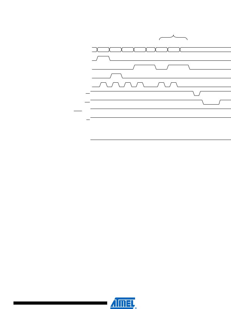
Figure 138. Programming the EEPROM Waveforms
|
|
|
|
|
|
|
K |
|
|
|
A |
G |
B |
C |
E |
B |
C |
E |
L |
DATA |
0x11 |
ADDR. HIGH ADDR. LOW |
DATA |
XX |
ADDR. LOW |
DATA |
XX |
|
|
|
|
|
|
|
|
|
|
|
|
XA1
XA0
BS1
XTAL1
WR
RDY/BSY
RESET +12V
OE
PAGEL
BS2
Reading the Flash |
The algorithm for reading the Flash memory is as follows (refer to “Programming the Flash” on |
|||||||
|
page 293 for details on Command and Address loading): |
|||||||
|
1. |
A: Load Command “0000 0010”. |
||||||
|
2. |
G: Load Address High Byte ($00 - $FF). |
||||||
|
3. |
B: Load Address Low Byte ($00 - $FF). |
||||||
|
4. |
Set |
|
|
to “0”, and BS1 to “0”. The Flash word low byte can now be read at DATA. |
|||
|
OE |
|||||||
|
5. |
Set BS1 to “1”. The Flash word high byte can now be read at DATA. |
||||||
|
6. |
Set |
|
|
to “1”. |
|||
|
OE |
|||||||
Reading the EEPROM |
The algorithm for reading the EEPROM memory is as follows (refer to “Programming the Flash” |
|||||||
|
on page 293 for details on Command and Address loading): |
|||||||
|
1. |
A: Load Command “0000 0011”. |
||||||
|
2. |
G: Load Address High Byte ($00 - $FF). |
||||||
|
3. |
B: Load Address Low Byte ($00 - $FF). |
||||||
|
4. |
Set |
|
|
to “0”, and BS1 to “0”. The EEPROM Data byte can now be read at DATA. |
|||
|
OE |
|||||||
|
5. |
Set |
|
|
to “1”. |
|||
|
OE |
|||||||
Programming the |
The algorithm for programming the Fuse Low bits is as follows (refer to “Programming the Flash” |
|||||||
Fuse Low Bits |
on page 293 for details on Command and Data loading): |
|||||||
|
1. |
A: Load Command “0100 0000”. |
||||||
|
2. |
C: Load Data Low Byte. Bit n = “0” programs and bit n = “1” erases the Fuse bit. |
||||||
|
3. |
Set BS1 to “0” and BS2 to “0”. |
||||||
|
4. |
Give |
|
|
|
to go high. |
||
|
WR |
a negative pulse and wait for RDY/BSY |
||||||
296
2467X–AVR–06/11

 ATmega128
Programming the |
The algorithm for programming the Fuse High bits is as follows (refer to “Programming the |
|||||
Fuse High Bits |
Flash” on page 293 for details on Command and Data loading): |
|||||
|
1. |
A: Load Command “0100 0000”. |
||||
|
2. |
C: Load Data Low Byte. Bit n = “0” programs and bit n = “1” erases the Fuse bit. |
||||
|
3. |
Set BS1 to “1” and BS2 to “0”. This selects high data byte. |
||||
|
4. |
Give |
|
|
|
to go high. |
|
WR |
a negative pulse and wait for RDY/BSY |
||||
|
5. |
Set BS1 to “0”. This selects low data byte. |
||||
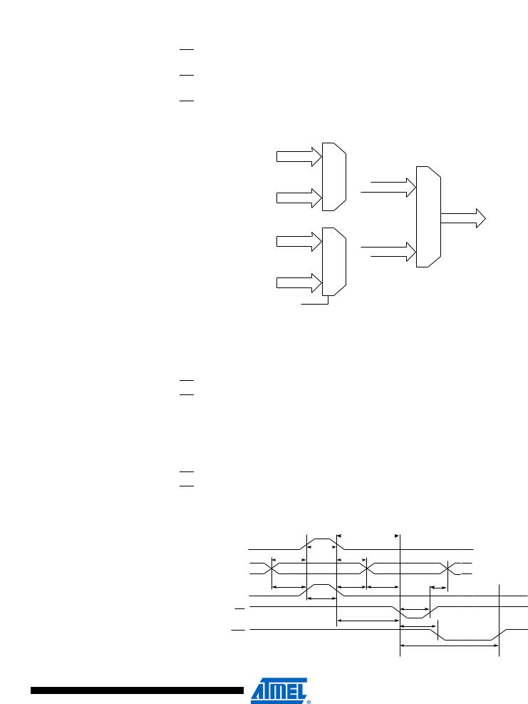
Programming the The algorithm for programming the Extended Fuse bits is as follows (refer to “Programming the Extended Fuse Bits Flash” on page 293 for details on Command and Data loading):
1.A: Load Command “0100 0000”.
2.C: Load Data Low Byte. Bit n = “0” programs and bit n = “1” erases the Fuse bit.
3.Set BS2 to “1” and BS1 to “0”. This selects extended data byte.
4.Give WR a negative pulse and wait for RDY/BSY to go high.
5.Set BS2 to “0”. This selects low data byte.
Figure 139. Programming the Fuses
|
|
|
Write Fuse Low byte |
|
|
Write Fuse high byte |
|
|
Write Extended Fuse byte |
|
A |
C |
|
A |
C |
|
A |
C |
|
DATA |
$40 |
DATA |
XX |
$40 |
DATA |
XX |
$40 |
DATA |
XX |
|
|
|
|
|
|
|
|
|
|
XA1 |
|
|
|
|
|
|
|
|
|
XA0 |
|
|
|
|
|
|
|
|
|
BS1 |
|
|
|
|
|
|
|
|
|
BS2 |
|
|
|
|
|
|
|
|
|
XTAL1 |
|
|
|
|
|
|
|
|
|
WR |
|
|
|
|
|
|
|
|
|
RDY/BSY |
|
|
|
|
|
|
|
|
|
RESET +12V |
|
|
|
|
|
|
|
|
|
OE |
|
|
|
|
|
|
|
|
|
PAGEL |
|
|
|
|
|
|
|
|
|
Programming the Lock The algorithm for programming the Lock bits is as follows (refer to “Programming the Flash” on Bits page 293 for details on Command and Data loading):
1.A: Load Command “0010 0000”.
2.C: Load Data Low Byte. Bit n = “0” programs the Lock bit.
3.Give WR a negative pulse and wait for RDY/BSY to go high.
The Lock bits can only be cleared by executing Chip Erase.
Reading the Fuse and The algorithm for reading the Fuse and Lock bits is as follows (refer to “Programming the Flash” Lock Bits on page 293 for details on Command loading):
1.A: Load Command “0000 0100”.
2.Set OE to “0”, BS2 to “0”, and BS1 to “0”. The status of the Fuse Low bits can now be read at DATA (“0” means programmed).
3.Set OE to “0”, BS2 to “1”, and BS1 to “1”. The status of the Fuse High bits can now be read at DATA (“0” means programmed).
297
2467X–AVR–06/11
 ATmega128
4.Set OE to “0”, BS2 to “1”, and BS1 to “0”. The status of the Extended Fuse bits can now be read at DATA (“0” means programmed).
5.Set OE to “0”, BS2 to “0”, and BS1 to “1”. The status of the Lock bits can now be read at DATA (“0” means programmed).
6.Set OE to “1”.
Figure 140. Mapping Between BS1, BS2 and the Fuseand Lock Bits During Read
Fuse Low Byte |
0 |
|
|
|
|
|
|||
|
|
|
|
||||||
|
|
||||||||
|
|
|
|
|
|
0 |
|||
|
|
|
|
|
|
||||
Extended Fuse byte |
1 |
|
|
|
|
|
|||
|
BS2 |
|
|
|
|
|
|
DATA |
|
|
|
|
|
|
|
|
|||
|
|
|
|||||||
|
|
|
|||||||
|
|
|
|
|
|
|
|
|
|
Lock bits |
0 |
|
|
|
|
|
|||
|
|
|
|
|
|
|
|
||
|
|
|
|
|
1 |
||||
|
|||||||||
|
|
|
|
|
|
BS1 |
|
||
|
|
|
|
|
|
|
|||
|
|
|
|
|
|
|
|||
Fuse high byte |
1 |
||||||||
|
|
|
|
|
|||||
|
|
|
|
|
|||||
|
|
|
|
|
|
|
|
|
|
BS2
Reading the Signature The algorithm for reading the Signature bytes is as follows (refer to Programming the Flash for Bytes details on Command and Address loading):
1.A: Load Command “0000 1000”.
2.B: Load Address Low Byte ($00 - $02).
3.Set OE to “0”, and BS1 to “0”. The selected Signature byte can now be read at DATA.
4.Set OE to “1”.
Reading the |
The algorithm for reading the Calibration byte is as follows (refer to Programming the Flash for |
Calibration Byte |
details on Command and Address loading): |
1.A: Load Command “0000 1000”.
2.B: Load Address Low Byte.
3.Set OE to “0”, and BS1 to “1”. The Calibration byte can now be read at DATA.
4.Set OE to “1”.
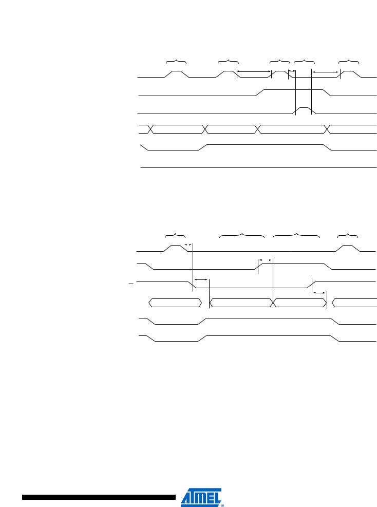
Parallel Programming Figure 141. Parallel Programming Timing, Including some General Timing Requirements |
||||||||||
Characteristics |
|
|
t XLWL |
|
||||||
|
|
|
|
|
||||||
XTAL1 |
tXHXL |
|||||||||
|
|
|
|
|
|
|
|
|||
Data & Contol |
tDVXH |
|
|
tXLDX |
|
|
||||
|
|
|
|
|
|
|
|
|
|
|
|
|
|
|
|
|
|
|
|
|
|
(DATA, XA0/1, BS1, BS2) |
|
|
|
|
|
|
|
|
||
tBVPH |
tPLBX |
t BVWL |
tWLBX |
PAGEL |
tPHPL |
|
|
|
|
||
|
|
|
tWL WH |
WR |
t PLWL |
|
WLRL |
|
|
|
|
RDY/BSY |
|
|
|
|
|
|
tWLRH |
298
2467X–AVR–06/11
 ATmega128
Figure 142. Parallel Programming Timing, Loading Sequence with Timing Requirements
LOAD ADDRESS |
LOAD DATA |
LOAD DATA LOAD DATA |
LOAD ADDRESS |
(LOW BYTE) |
(LOW BYTE) |
(HIGH BYTE) |
(LOW BYTE) |
|
t XLXH |
tXLPH |
tPLXH |
|
|
XTAL1
BS1
PAGEL
DATA |
ADDR0 (Low Byte) |
DATA (Low Byte) |
DATA (High Byte) |
ADDR1 (Low Byte) |
XA0
XA1
Note: The timing requirements shown in Figure 141 (i.e. tDVXH, tXHXL, and tXLDX) also apply to loading operation.
Figure 143. Parallel Programming Timing, Reading Sequence (Within the Same Page) with Timing Requirements
LOAD ADDRESS |
READ DATA |
|
|
READ DATA |
LOAD ADDRESS |
|||
(LOW BYTE) |
(LOW BYTE) |
|
|
(HIGH BYTE) |
(LOW BYTE) |
|||
|
tXLOL |
|
|
|
|
|
||
XTAL1 |
|
|
|
|
|
|
|
|
|
|
|
|
|
tBHDV |
|
||
|
|
|
|
|
|
|
|
|
BS1
tOLDV
OE
tOHDZ
DATA |
|
ADDR0 (Low Byte) |
|
DATA (Low Byte) |
DATA (High Byte) |
|
ADDR1 (Low Byte) |
|
|
|
XA0
XA1
Note: The timing requirements shown in Figure 141 (i.e. tDVXH, tXHXL, and tXLDX) also apply to reading operation.
Table 126. |
Parallel Programming Characteristics, VCC = 5 V ±10% |
|
|
||||
Symbol |
Parameter |
Min |
Typ |
Max |
Units |
||
|
|
|
|
|
|
||
VPP |
Programming Enable Voltage |
11.5 |
|
12.5 |
V |
||
IPP |
Programming Enable Current |
|
|
250 |
μA |
||
tDVXH |
Data and Control Valid before XTAL1 High |
67 |
|
|
ns |
||
tXLXH |
XTAL1 Low to XTAL1 High |
200 |
|
|
ns |
||
tXHXL |
XTAL1 Pulse Width High |
150 |
|
|
ns |
||
tXLDX |
Data and Control Hold after XTAL1 Low |
67 |
|
|
ns |
||
tXLWL |
XTAL1 Low to |
|
Low |
0 |
|
|
ns |
WR |
|
||||||
299
2467X–AVR–06/11

 ATmega128
Serial
Downloading
Table 126. |
|
Parallel Programming Characteristics, VCC = 5 V ±10% |
(Continued) |
|
|
||||||||||||||||||
Symbol |
|
|
Parameter |
Min |
Typ |
Max |
|
Units |
|
||||||||||||||
|
|
|
|
|
|
|
|
|
|
|
|||||||||||||
tXLPH |
|
|
XTAL1 Low to PAGEL high |
0 |
|
|
|
|
ns |
|
|||||||||||||
tPLXH |
|
|
PAGEL low to XTAL1 high |
150 |
|
|
|
|
ns |
|
|||||||||||||
tBVPH |
|
|
BS1 Valid before PAGEL High |
67 |
|
|
|
|
ns |
|
|||||||||||||
tPHPL |
|
|
PAGEL Pulse Width High |
150 |
|
|
|
|
ns |
|
|||||||||||||
tPLBX |
|
|
BS1 Hold after PAGEL Low |
67 |
|
|
|
|
ns |
|
|||||||||||||
tWLBX |
|
|
BS2/1 Hold after |
|
|
|
|
Low |
67 |
|
|
|
|
ns |
|
||||||||
WR |
|
|
|
||||||||||||||||||||
tPLWL |
|
|
PAGEL Low to |
|
|
|
|
|
Low |
67 |
|
|
|
|
ns |
|
|||||||
WR |
|
|
|
||||||||||||||||||||
tBVWL |
|
|
BS1 Valid to |
|
|
|
|
Low |
67 |
|
|
|
|
ns |
|
||||||||
WR |
|
|
|
||||||||||||||||||||
tWLWH |
|
|
|
|
|
Pulse Width Low |
150 |
|
|
|
|
ns |
|
||||||||||
|
|
WR |
|
|
|
||||||||||||||||||
tWLRL |
|
|
|
|
|
|
|
|
|
|
|
|
|
|
|
Low |
0 |
|
|
1 |
|
μs |
|
|
|
WR |
Low to RDY/BSY |
||||||||||||||||||||
tWLRH |
|
|
|
|
|
|
|
|
|
|
|
|
|
|
|
High(1) |
3.7 |
|
|
5 |
|
ms |
|
|
|
WR |
Low to RDY/BSY |
||||||||||||||||||||
tWLRH_CE |
|
|
|
|
|
|
|
|
|
|
|
|
|
|
|
High for Chip Erase(2) |
7.5 |
|
|
10 |
|
ms |
|
|
|
WR |
Low to RDY/BSY |
||||||||||||||||||||
tXLOL |
|
|
XTAL1 Low to |
|
|
|
|
|
Low |
0 |
|
|
|
|
ns |
|
|||||||
|
|
OE |
|
|
|
||||||||||||||||||
tBVDV |
|
|
BS1 Valid to DATA valid |
0 |
|
|
250 |
|
ns |
|
|||||||||||||
tOLDV |
|
|
|
Low to DATA Valid |
|
|
|
250 |
|
ns |
|
||||||||||||
|
|
OE |
|
|
|||||||||||||||||||
tOHDZ |
|
|
|
High to DATA Tri-stated |
|
|
|
250 |
|
ns |
|
||||||||||||
|
|
OE |
|
|
|||||||||||||||||||
Notes: 1. tWLRH is valid for the Write Flash, Write EEPROM, Write |
Fuse bits and |
Write Lock bits |
|||||||||||||||||||||
|
commands. |
|
|
|
|
|
|
|
|||||||||||||||
2.tWLRH_CE is valid for the Chip Erase command.
Both the Flash and EEPROM memory arrays can be programmed using the serial SPI bus while RESET is pulled to GND. The serial interface consists of pins SCK, MOSI (input) and MISO (out-
put). After RESET is set low, the Programming Enable instruction needs to be executed first before program/erase operations can be executed. NOTE, in Table 127 on page 300, the pin mapping for SPI programming is listed. Not all parts use the SPI pins dedicated for the internal SPI interface. Note that throughout the description about Serial downloading, MOSI and MISO are used to describe the serial data in and serial data out respectively. For Atmel® AVR®ATmega128 these pins are mapped to PDI and PDO.
SPI Serial
Programming Pin
Mapping
Even though the SPI Programming interface re-uses the SPI I/O module, there is one important difference: The MOSI/MISO pins that are mapped to PB2 and PB3 in the SPI I/O module are not used in the Programming interface. Instead, PE0 and PE1 are used for data in SPI Programming mode as shown in Table 127.
Table 127. Pin Mapping SPI Serial Programming
Symbol |
Pins |
I/O |
Description |
|
|
|
|
MOSI (PDI) |
PE0 |
I |
Serial data in |
|
|
|
|
MISO (PDO) |
PE1 |
O |
Serial data out |
|
|
|
|
SCK |
PB1 |
I |
Serial clock |
|
|
|
|
300
2467X–AVR–06/11
SPI Serial
Programming
Algorithm
ATmega128
Figure 144. SPI Serial Programming and Verify(1)
+2.7 - 5.5V
VCC
+2.7 - 5.5V(2)
PDI  PE0
PE0
AVCC
PDO  PE1
PE1
SCK  PB1
PB1
 XTAL1
XTAL1
RESET
GND
Notes: 1. If the device is clocked by the Internal Oscillator, it is no need to connect a clock source to the XTAL1 pin.
2. VCC - 0.3V < AVCC < VCC + 0.3V, however, AVCC should always be within 2.7 - 5.5V.
When programming the EEPROM, an auto-erase cycle is built into the self-timed programming operation (in the serial mode ONLY) and there is no need to first execute the Chip Erase instruction. The Chip Erase operation turns the content of every memory location in both the Program and EEPROM arrays into $FF.
Depending on CKSEL Fuses, a valid clock must be present. The minimum low and high periods for the serial clock (SCK) input are defined as follows:
Low:> 2 CPU clock cycles for fck < 12MHz, 3 CPU clock cycles for fck ≥ 12MHz High:> 2 CPU clock cycles for fck < 12MHz, 3 CPU clock cycles for fck ≥ 12MHz
When writing serial data to the ATmega128, data is clocked on the rising edge of SCK.
When reading data from the ATmega128, data is clocked on the falling edge of SCK. See Figure 145 for timing details.
To program and verify the ATmega128 in the SPI Serial Programming mode, the following sequence is recommended (See four byte instruction formats in Table 145):
1.Power-up sequence:
Apply power between VCC and GND while RESET and SCK are set to “0”. In some systems, the programmer can not guarantee that SCK is held low during power-up. In this case, RESET must be given a positive pulse of at least two CPU clock cycles duration after SCK has been set to “0”.
As an alternative to using the RESET signal, PEN can be held low during Power-on Reset while SCK is set to “0”. In this case, only the PEN value at Power-on Reset is important. If the programmer cannot guarantee that SCK is held low during power-up, the PEN method cannot be used. The device must be powered down in order to commence normal operation when using this method.
2.Wait for at least 20 ms and enable SPI Serial Programming by sending the Programming Enable serial instruction to pin MOSI.
301
2467X–AVR–06/11