

- •Features
- •Overview
- •Block Diagram
- •Pin Descriptions
- •Port A (PA7..PA0)
- •Port B (PB7..PB0)
- •Port C (PC7..PC0)
- •Port D (PD7..PD0)
- •Port E (PE7..PE0)
- •Port F (PF7..PF0)
- •Port G (PG4..PG0)
- •RESET
- •XTAL1
- •XTAL2
- •AVCC
- •AREF
- •Resources
- •Data Retention
- •Capacitive touch sensing
- •AVR CPU Core
- •Introduction
- •Status Register
- •Stack Pointer
- •I/O Memory
- •Overview
- •Timing
- •Using all Locations of External Memory Smaller than 64 Kbyte
- •Clock Systems and their Distribution
- •CPU Clock – clkCPU
- •I/O Clock – clkI/O
- •Flash Clock – clkFLASH
- •ADC Clock – clkADC
- •Clock Sources
- •Crystal Oscillator
- •External Clock
- •Idle Mode
- •Power-down Mode
- •Power-save Mode
- •Standby Mode
- •Analog Comparator
- •Brown-out Detector
- •Watchdog Timer
- •Port Pins
- •Resetting the AVR
- •Reset Sources
- •Power-on Reset
- •External Reset
- •Watchdog Reset
- •Watchdog Timer
- •Timed Sequences for Changing the Configuration of the Watchdog Timer
- •Safety Level 0
- •Safety Level 1
- •Safety Level 2
- •Interrupts
- •I/O Ports
- •Introduction
- •Configuring the Pin
- •Reading the Pin Value
- •Unconnected pins
- •Alternate Port Functions
- •Register Description for I/O Ports
- •8-bit Timer/Counter0 with PWM and Asynchronous Operation
- •Overview
- •Registers
- •Definitions
- •Counter Unit
- •Normal Mode
- •Fast PWM Mode
- •8-bit Timer/Counter Register Description
- •Overview
- •Registers
- •Definitions
- •Compatibility
- •Counter Unit
- •Input Capture Unit
- •Noise Canceler
- •Force Output Compare
- •Normal Mode
- •Fast PWM Mode
- •16-bit Timer/Counter Register Description
- •Internal Clock Source
- •Prescaler Reset
- •External Clock Source
- •8-bit Timer/Counter2 with PWM
- •Overview
- •Registers
- •Definitions
- •Counter Unit
- •Normal Mode
- •Fast PWM Mode
- •8-bit Timer/Counter Register Description
- •Output Compare Modulator (OCM1C2)
- •Overview
- •Description
- •Timing Example
- •Slave Mode
- •Master Mode
- •Data Modes
- •USART
- •Dual USART
- •Overview
- •AVR USART vs. AVR UART – Compatibility
- •Clock Generation
- •External Clock
- •Frame Formats
- •Parity Bit Calculation
- •Parity Generator
- •Receiver Error Flags
- •Parity Checker
- •Disabling the Receiver
- •Using MPCM
- •Features
- •TWI Terminology
- •Transferring Bits
- •Address Packet Format
- •Data Packet Format
- •Overview of the TWI Module
- •Scl and SDA Pins
- •Bus Interface Unit
- •Address Match Unit
- •Control Unit
- •Using the TWI
- •Master Receiver Mode
- •Slave Receiver Mode
- •Miscellaneous States
- •Analog Comparator
- •Analog to Digital Converter
- •Features
- •Operation
- •Changing Channel or Reference Selection
- •ADC Input Channels
- •Analog Input Circuitry
- •Features
- •Overview
- •TAP Controller
- •PRIVATE0; $8
- •PRIVATE1; $9
- •PRIVATE2; $A
- •PRIVATE3; $B
- •Bibliography
- •Features
- •System Overview
- •Data Registers
- •Bypass Register
- •Reset Register
- •EXTEST; $0
- •IDCODE; $1
- •AVR_RESET; $C
- •BYPASS; $F
- •Scanning the ADC
- •ATmega128 Boundary-scan Order
- •Application Section
- •Programming Time for Flash when Using SPM
- •Simple Assembly Code Example for a Boot Loader
- •Fuse Bits
- •Latching of Fuses
- •Signature Bytes
- •Calibration Byte
- •Signal Names
- •Chip Erase
- •Reading the Flash
- •Reading the EEPROM
- •Data Polling Flash
- •Data Polling EEPROM
- •AVR_RESET ($C)
- •PROG_ENABLE ($4)
- •Data Registers
- •Reset Register
- •Programming Enable Register
- •Programming Command Register
- •Virtual Flash Page Read Register
- •Performing Chip Erase
- •Reading the Flash
- •Reading the EEPROM
- •Electrical Characteristics
- •Absolute Maximum Ratings*
- •DC Characteristics
- •Speed Grades
- •External Clock Drive Waveforms
- •External Clock Drive
- •Two-wire Serial Interface Characteristics
- •ADC Characteristics
- •External Data Memory Timing
- •Idle Supply Current
- •Pin Pull-up
- •Pin Driver Strength
- •Register Summary
- •Instruction Set Summary
- •Ordering Information
- •Packaging Information
- •Errata
- •ATmega128 Rev. F to M
 ATmega128
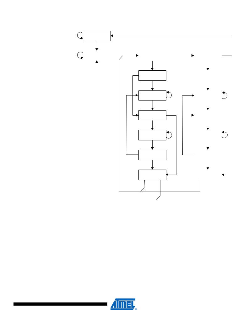
Figure 146. State Machine Sequence for Changing the Instruction Word
1 |
Test-Logic-Reset |
|
|
|
|
|
|
|
|
|
|
|
|
|
0 |
|
|
|
|
|
|
|
|
|
|
|
|
0 |
|
|
1 |
|
|
|
1 |
|
|
|
|
|
1 |
Run-Test/Idle |
|
Select-DR Scan |
|
Select-IR Scan |
|||||||||
|
|
|
|
|
|
||||||||
|
|
|
|
|
|
|
|
|
|
|
|
|
|
|
|
|
|
|
0 |
|
|
|
|
0 |
|
|
|
|
|
|
|
1 |
Capture-DR |
|
|
1 |
|
|
|
|
|
|
|
|
|
|
|
|
|
|
|
|
|||
|
|
|
|
|
|
Capture-IR |
|
|
|||||
|
|
|
|
|
|
|
|
|
|
||||
|
|
|
|
|
|
|
|
|
|
|
|
|
|
|
|
|
|
|
0 |
|
|
|
|
0 |
|
|
|
|
|
|
|
|
|
|
|
|
|
|
|
|
|
|
|
|
|
|
|
|
|
|
|
|
|
|
|
|
|
|
|
|
Shift-DR |
|
0 |
|
Shift-IR |
|
0 |
||
|
|
|
|
|
|
|
|
|
|
|
|
|
|
|
|
|
|
|
1 |
|
|
|
|
1 |
|
|
|
|
|
|
|
|
Exit1-DR |
|
1 |
|
|
|
|
|
|
|
|
|
|
|
|
|
|
|
|
|
1 |
||
|
|
|
|
|
|
|
Exit1-IR |
|
|||||
|
|
|
|
|
|
|
|
|
|
||||
|
|
|
|
|
|
|
|
|
|
|
|
|
|
|
|
|
|
|
0 |
|
|
|
|
0 |
|
|
|
|
|
|
|
|
Pause-DR |
|
0 |
|
|
|
|
|
|
|
|
|
|
|
|
|
|
|
|
|
0 |
||
|
|
|
|
|
|
|
Pause-IR |
|
|||||
|
|
|
|
|
|
|
|
|
|
|
|
|
|
|
|
|
|
|
1 |
|
|
|
|
1 |
|
|
|
|
|
|
|
0 |
Exit2-DR |
|
|
0 |
|
|
|
|
|
|
|
|
|
|
|
Exit2-IR |
|
|
|||||
|
|
|
|
|
|
|
|
|
|
||||
|
|
|
|
|
|
|
|
|
|
|
|
|
|
|
|
|
|
|
1 |
|
|
|
|
1 |
|
|
|
|
|
|
|
|
Update-DR |
|
|
|
|
|
|
|
|
|
|
|
|
|
|
|
|
Update-IR |
|
|
|||
|
|
|
|
|
|
|
|
|
|
||||
|
|
|
|
|
|
|
|
|
|
|
|
|
|
|
|
|
|
|
1 |
0 |
|
|
1 |
|
|
0 |
|
|
|
|
|
|
|
|
|
|
|
|
|
|
|
AVR_RESET ($C) |
The AVR specific public JTAG instruction for setting the AVR device in the Reset mode or taking |
|
the device out from the Reset mode. The TAP controller is not reset by this instruction. The one |
|
bit Reset Register is selected as Data Register. Note that the reset will be active as long as there |
|
is a logic 'one' in the Reset Chain. The output from this chain is not latched. |
The active states are:
•Shift-DR: The Reset Register is shifted by the TCK input.
PROG_ENABLE ($4) The AVR specific public JTAG instruction for enabling programming via the JTAG port. The 16bit Programming Enable Register is selected as data register. The active states are the following:
•Shift-DR: the programming enable signature is shifted into the data register.
•Update-DR: the programming enable signature is compared to the correct value, and Programming mode is entered if the signature is valid.
306
2467X–AVR–06/11

 ATmega128
PROG_COMMANDS The AVR specific public JTAG instruction for entering programming commands via the JTAG ($5) port. The 15-bit Programming Command Register is selected as data register. The active states
are the following:
•Capture-DR: the result of the previous command is loaded into the data register.
•Shift-DR: the data register is shifted by the TCK input, shifting out the result of the previous command and shifting in the new command.
•Update-DR: the programming command is applied to the Flash inputs.
•Run-Test/Idle: one clock cycle is generated, executing the applied command.
PROG_PAGELOAD The AVR specific public JTAG instruction to directly load the Flash data page via the JTAG port. ($6) The 2048-bit Virtual Flash Page Load Register is selected as data register. This is a virtual scan chain with length equal to the number of bits in one Flash page. Internally the Shift Register is 8- bit. Unlike most JTAG instructions, the Update-DR state is not used to transfer data from the Shift Register. The data are automatically transferred to the Flash page buffer byte by byte in the
Shift-DR state by an internal state machine. This is the only active state:
•Shift-DR: Flash page data are shifted in from TDI by the TCK input, and automatically loaded into the Flash page one byte at a time.
Note: The JTAG instruction PROG_PAGELOAD can only be used if the AVR device is the first device in JTAG scan chain. If the AVR cannot be the first device in the scan chain, the byte-wise programming algorithm must be used.
PROG_PAGEREAD |
The AVR specific public JTAG instruction to read one full Flash data page via the JTAG port. |
|
($7) |
The 2056-bit Virtual Flash Page Read Register is selected as data register. This is a virtual scan |
|
|
chain with length equal to the number of bits in one Flash page plus 8. Internally the Shift Regis- |
|
|
ter is 8-bit. Unlike most JTAG instructions, the Capture-DR state is not used to transfer data to |
|
|
the Shift Register. The data are automatically transferred from the Flash page buffer byte by |
|
|
byte in the Shift-DR state by an internal state machine. This is the only active state: |
|
|
• Shift-DR: Flash data are automatically read one byte at a time and shifted out on TDO by the |
|
|
|
TCK input. The TDI input is ignored. |
|
Note: The JTAG instruction PROG_PAGEREAD can only be used if the AVR device is the first device in |
|
|
|
JTAG scan chain. If the AVR cannot be the first device in the scan chain, the byte-wise program- |
|
|
ming algorithm must be used. |
Data Registers |
The data registers are selected by the JTAG instruction registers described in section “Program- |
|
|
ming Specific JTAG Instructions” on page 305. The data registers relevant for programming |
|
|
operations are: |
|
|
• |
Reset Register |
|
• |
Programming Enable Register |
|
• |
Programming Command Register |
• Virtual Flash Page Load Register
• Virtual Flash Page Read Register
307
2467X–AVR–06/11

 ATmega128
Reset Register |
The Reset Register is a Test Data Register used to reset the part during programming. It is |
|
required to reset the part before entering programming mode. |
|
A high value in the Reset Register corresponds to pulling the external Reset low. The part is |
|
reset as long as there is a high value present in the Reset Register. Depending on the Fuse set- |
|
tings for the clock options, the part will remain reset for a Reset Time-Out Period (refer to “Clock |
|
Sources” on page 36) after releasing the Reset Register. The output from this Data Register is |
|
not latched, so the reset will take place immediately, as shown in Figure 123 on page 254. |
Programming Enable |
The Programming Enable Register is a 16-bit register. The contents of this register is compared |
Register |
to the programming enable signature, binary code 1010_0011_0111_0000. When the contents |
|
of the register is equal to the programming enable signature, programming via the JTAG port is |
|
enabled. The Register is reset to 0 on Power-on Reset, and should always be reset when leav- |
|
ing Programming mode. |
|
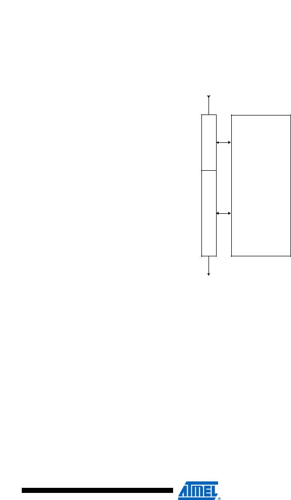
Figure 147. Programming Enable Register |
|
TDI |
|
|
$A370 |
|
|
|
|
|
|
|
|
|
|
|
|
|
|
|
|
|
||
D |
= |
|
|
D |
Q |
|
Programming enable |
|||
|
|
|
|
|
||||||
A |
|
|
|
|
|
|||||
|
|
|
|
|
|
|||||
T |
|
|
|
|
|
|
|
|
|
|
A |
|
|
|
|
|
|
|
|
|
|
|
|
|
|
|
|
|
|
|
||
|
|
|
|
|
|
|
|
|
||
|
|
|
|
|
|
|
|
|
|
|
|
|
|
|
ClockDR & PROG_ENABLE |
|
|
||||
|
|
|
|
|
|
|
|
|
|
|
|
|
|
|
|
|
|
|
|
|
|
TDO
308
2467X–AVR–06/11
 ATmega128
Programming |
The Programming Command Register is a 15-bit register. This register is used to serially shift in |
Command Register |
programming commands, and to serially shift out the result of the previous command, if any. The |
|
JTAG Programming Instruction Set is shown in Table 130. The state sequence when shifting in |
|
the programming commands is illustrated in Figure 149. |
|
Figure 148. Programming Command Register |
TDI
S
T
R
O
B
E
S
A
D
D
R
E
S
S
/
D
A
T
A
Flash
EEPROM
Fuses
Lock Bits
TDO
309
2467X–AVR–06/11

 ATmega128
Table 130. JTAG Programming Instruction
Set a = address high bits, b = address low bits, H = 0 - Low Byte, 1 - High Byte, o = data out, i = data in, x = don’t care
Instruction |
TDI sequence |
TDO sequence |
Notes |
|
|
|
|
|
|
1a. |
Chip erase |
0100011_10000000 |
xxxxxxx_xxxxxxxx |
|
|
|
0110001_10000000 |
xxxxxxx_xxxxxxxx |
|
|
|
0110011_10000000 |
xxxxxxx_xxxxxxxx |
|
|
|
0110011_10000000 |
xxxxxxx_xxxxxxxx |
|
|
|
|
|
|
1b. Poll for chip erase complete |
0110011_10000000 |
xxxxxox_xxxxxxxx |
(2) |
|
|
|
|
|
|
2a. |
Enter Flash Write |
0100011_00010000 |
xxxxxxx_xxxxxxxx |
|
|
|
|
|
|
2b. Load Address High Byte |
0000111_aaaaaaaa |
xxxxxxx_xxxxxxxx |
(9) |
|
|
|
|
|
|
2c. Load Address Low Byte |
0000011_bbbbbbbb |
xxxxxxx_xxxxxxxx |
|
|
|
|
|
|
|
2d. |
Load Data Low Byte |
0010011_iiiiiiii |
xxxxxxx_xxxxxxxx |
|
|
|
|
|
|
2e. |
Load Data High Byte |
0010111_iiiiiiii |
xxxxxxx_xxxxxxxx |
|
|
|
|
|
|
2f. Latch Data |
0110111_00000000 |
xxxxxxx_xxxxxxxx |
(1) |
|
|
|
1110111_00000000 |
xxxxxxx_xxxxxxxx |
|
|
|
0110111_00000000 |
xxxxxxx_xxxxxxxx |
|
|
|
|
|
|
2g. |
Write Flash Page |
0110111_00000000 |
xxxxxxx_xxxxxxxx |
(1) |
|
|
0110101_00000000 |
xxxxxxx_xxxxxxxx |
|
|
|
0110111_00000000 |
xxxxxxx_xxxxxxxx |
|
|
|
0110111_00000000 |
xxxxxxx_xxxxxxxx |
|
|
|
|
|
|
2h. |
Poll for Page Write complete |
0110111_00000000 |
xxxxxox_xxxxxxxx |
(2) |
|
|
|
|
|
3a. |
Enter Flash Read |
0100011_00000010 |
xxxxxxx_xxxxxxxx |
|
|
|
|
|
|
3b. Load Address High Byte |
0000111_aaaaaaaa |
xxxxxxx_xxxxxxxx |
(9) |
|
|
|
|
|
|
3c. Load Address Low Byte |
0000011_bbbbbbbb |
xxxxxxx_xxxxxxxx |
|
|
|
|
|
|
|
3d. |
Read Data Low and High Byte |
0110010_00000000 |
xxxxxxx_xxxxxxxx |
|
|
|
0110110_00000000 |
xxxxxxx_oooooooo |
low byte |
|
|
0110111_00000000 |
xxxxxxx_oooooooo |
high byte |
|
|
|
|
|
4a. |
Enter EEPROM Write |
0100011_00010001 |
xxxxxxx_xxxxxxxx |
|
|
|
|
|
|
4b. Load Address High Byte |
0000111_aaaaaaaa |
xxxxxxx_xxxxxxxx |
(9) |
|
|
|
|
|
|
4c. Load Address Low Byte |
0000011_bbbbbbbb |
xxxxxxx_xxxxxxxx |
|
|
|
|
|
|
|
4d. |
Load Data Byte |
0010011_iiiiiiii |
xxxxxxx_xxxxxxxx |
|
|
|
|
|
|
4e. |
Latch Data |
0110111_00000000 |
xxxxxxx_xxxxxxxx |
(1) |
|
|
1110111_00000000 |
xxxxxxx_xxxxxxxx |
|
|
|
0110111_00000000 |
xxxxxxx_xxxxxxxx |
|
|
|
|
|
|
4f. Write EEPROM Page |
0110011_00000000 |
xxxxxxx_xxxxxxxx |
(1) |
|
|
|
0110001_00000000 |
xxxxxxx_xxxxxxxx |
|
|
|
0110011_00000000 |
xxxxxxx_xxxxxxxx |
|
|
|
0110011_00000000 |
xxxxxxx_xxxxxxxx |
|
|
|
|
|
|
4g. |
Poll for Page Write complete |
0110011_00000000 |
xxxxxox_xxxxxxxx |
(2) |
|
|
|
|
|
5a. |
Enter EEPROM Read |
0100011_00000011 |
xxxxxxx_xxxxxxxx |
|
|
|
|
|
|
5b. Load Address High Byte |
0000111_aaaaaaaa |
xxxxxxx_xxxxxxxx |
(9) |
|
|
|
|
|
|
310
2467X–AVR–06/11
 ATmega128
Table 130. JTAG Programming Instruction |
(Continued) |
|
|
||
Set |
(Continued) a = address high bits, b = address low bits, H = 0 - Low Byte, 1 - High Byte, o = data out, i = data in, x = don’t care |
||||
|
|
|
|
|
|
Instruction |
|
TDI sequence |
TDO sequence |
Notes |
|
|
|
|
|
|
|
5c. Load Address Low Byte |
|
0000011_bbbbbbbb |
xxxxxxx_xxxxxxxx |
|
|
|
|
|
|
|
|
5d. |
Read Data Byte |
|
0110011_bbbbbbbb |
xxxxxxx_xxxxxxxx |
|
|
|
|
0110010_00000000 |
xxxxxxx_xxxxxxxx |
|
|
|
|
0110011_00000000 |
xxxxxxx_oooooooo |
|
|
|
|
|
|
|
6a. |
Enter Fuse Write |
|
0100011_01000000 |
xxxxxxx_xxxxxxxx |
|
|
|
|
|
|
|
6b. Load Data Low Byte(6) |
|
0010011_iiiiiiii |
xxxxxxx_xxxxxxxx |
(3) |
|
6c. Write Fuse Extended Byte |
|
0111011_00000000 |
xxxxxxx_xxxxxxxx |
(1) |
|
|
|
|
0111001_00000000 |
xxxxxxx_xxxxxxxx |
|
|
|
|
0111011_00000000 |
xxxxxxx_xxxxxxxx |
|
|
|
|
0111011_00000000 |
xxxxxxx_xxxxxxxx |
|
|
|
|
|
|
|
6d. |
Poll for Fuse Write complete |
|
0110111_00000000 |
xxxxxox_xxxxxxxx |
(2) |
|
|
|
|
|
|
6e. |
Load Data Low Byte(7) |
|
0010011_iiiiiiii |
xxxxxxx_xxxxxxxx |
(3) |
6f. Write Fuse High Byte |
|
0110111_00000000 |
xxxxxxx_xxxxxxxx |
(1) |
|
|
|
|
0110101_00000000 |
xxxxxxx_xxxxxxxx |
|
|
|
|
0110111_00000000 |
xxxxxxx_xxxxxxxx |
|
|
|
|
0110111_00000000 |
xxxxxxx_xxxxxxxx |
|
|
|
|
|
|
|
6g. |
Poll for Fuse Write complete |
|
0110111_00000000 |
xxxxxox_xxxxxxxx |
(2) |
|
|
|
|
|
|
6h. |
Load Data Low Byte(7) |
|
0010011_iiiiiiii |
xxxxxxx_xxxxxxxx |
(3) |
6i. Write Fuse Low Byte |
|
0110011_00000000 |
xxxxxxx_xxxxxxxx |
(1) |
|
|
|
|
0110001_00000000 |
xxxxxxx_xxxxxxxx |
|
|
|
|
0110011_00000000 |
xxxxxxx_xxxxxxxx |
|
|
|
|
0110011_00000000 |
xxxxxxx_xxxxxxxx |
|
|
|
|
|
|
|
6j. Poll for Fuse Write complete |
|
0110011_00000000 |
xxxxxox_xxxxxxxx |
(2) |
|
|
|
|
|
|
|
7a. |
Enter Lock bit Write |
|
0100011_00100000 |
xxxxxxx_xxxxxxxx |
|
|
|
|
|
|
|
7b. Load Data Byte(9) |
|
0010011_11iiiiii |
xxxxxxx_xxxxxxxx |
(4) |
|
7c. Write Lock bits |
|
0110011_00000000 |
xxxxxxx_xxxxxxxx |
(1) |
|
|
|
|
0110001_00000000 |
xxxxxxx_xxxxxxxx |
|
|
|
|
0110011_00000000 |
xxxxxxx_xxxxxxxx |
|
|
|
|
0110011_00000000 |
xxxxxxx_xxxxxxxx |
|
|
|
|
|
|
|
7d. |
Poll for Lock bit Write complete |
|
0110011_00000000 |
xxxxxox_xxxxxxxx |
(2) |
|
|
|
|
|
|
8a. |
Enter Fuse/Lock bit Read |
|
0100011_00000100 |
xxxxxxx_xxxxxxxx |
|
|
|
|
|
|
|
8b. Read Extended Fuse Byte(6) |
|
0111010_00000000 |
xxxxxxx_xxxxxxxx |
|
|
|
|
|
0111011_00000000 |
xxxxxxx_oooooooo |
|
|
|
|
|
|
|
8c. Read Fuse High Byte(7) |
|
0111110_00000000 |
xxxxxxx_xxxxxxxx |
|
|
|
|
|
0111111_00000000 |
xxxxxxx_oooooooo |
|
|
|
|
|
|
|
8d. |
Read Fuse Low Byte(8) |
|
0110010_00000000 |
xxxxxxx_xxxxxxxx |
|
|
|
|
0110011_00000000 |
xxxxxxx_oooooooo |
|
|
|
|
|
|
|
8e. |
Read Lock bits(9) |
|
0110110_00000000 |
xxxxxxx_xxxxxxxx |
(5) |
|
|
|
0110111_00000000 |
xxxxxxx_xxoooooo |
|
|
|
|
|
|
|
311
2467X–AVR–06/11

 ATmega128
Table 130. JTAG Programming Instruction (Continued)
Set (Continued) a = address high bits, b = address low bits, H = 0 - Low Byte, 1 - High Byte, o = data out, i = data in, x = don’t care
Instruction |
TDI sequence |
TDO sequence |
Notes |
|
|
|
|
8f. Read Fuses and Lock bits |
0111010_00000000 |
xxxxxxx_xxxxxxxx |
(5) |
|
0111110_00000000 |
xxxxxxx_oooooooo |
fuse ext. byte |
|
0110010_00000000 |
xxxxxxx_oooooooo |
fuse high byte |
|
0110110_00000000 |
xxxxxxx_oooooooo |
fuse low byte |
|
0110111_00000000 |
xxxxxxx_oooooooo |
lock bits |
|
|
|
|
9a. Enter Signature Byte Read |
0100011_00001000 |
xxxxxxx_xxxxxxxx |
|
|
|
|
|
9b. Load Address Byte |
0000011_bbbbbbbb |
xxxxxxx_xxxxxxxx |
|
|
|
|
|
9c. Read Signature Byte |
0110010_00000000 |
xxxxxxx_xxxxxxxx |
|
|
0110011_00000000 |
xxxxxxx_oooooooo |
|
|
|
|
|
10a. Enter Calibration Byte Read |
0100011_00001000 |
xxxxxxx_xxxxxxxx |
|
|
|
|
|
10b. Load Address Byte |
0000011_bbbbbbbb |
xxxxxxx_xxxxxxxx |
|
|
|
|
|
10c. Read Calibration Byte |
0110110_00000000 |
xxxxxxx_xxxxxxxx |
|
|
0110111_00000000 |
xxxxxxx_oooooooo |
|
|
|
|
|
11a. Load No Operation Command |
0100011_00000000 |
xxxxxxx_xxxxxxxx |
|
|
0110011_00000000 |
xxxxxxx_xxxxxxxx |
|
|
|
|
|
Notes: 1. This command sequence is not required if the seven MSB are correctly set by the previous command sequence (which is normally the case).
2.Repeat until o = “1”.
3.Set bits to “0” to program the corresponding fuse, “1” to unprogram the Fuse.
4.Set bits to “0” to program the corresponding lock bit, “1” to leave the Lock bit unchanged.
5.“0” = programmed, “1” = unprogrammed.
6.The bit mapping for Fuses Extended Byte is listed in Table 117 on page 287
7.The bit mapping for Fuses High Byte is listed in Table 118 on page 288
8.The bit mapping for Fuses Low Byte is listed in Table 119 on page 288
9.The bit mapping for Lock bits Byte is listed in Table 115 on page 286
10.Address bits exceeding PCMSB and EEAMSB (Table 123 and Table 124) are don’t care
312
2467X–AVR–06/11
 ATmega128
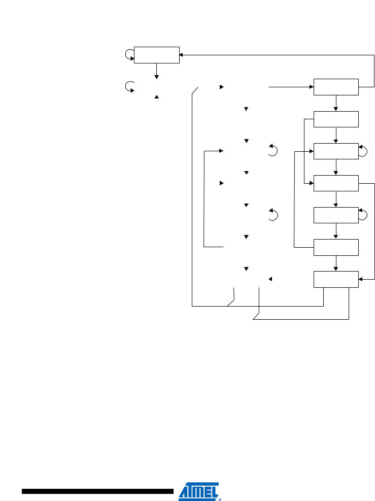
Figure 149. State Machine Sequence for Changing/Reading the Data Word
1 |
Test-Logic-Reset |
|
|
|
|
|
|
|
|
|
|
|
|
|
0 |
|
|
|
|
|
|
|
|
|
|
|
|
0 |
|
|
1 |
|
|
|
|
|
1 |
|
|
|
1 |
Run-Test/Idle |
|
Select-DR Scan |
|
Select-IR Scan |
|||||||||
|
|
|
|
|
|
||||||||
|
|
|
|
|
|
|
|
|
|
|
|
|
|
|
|
|
|
|
|
0 |
|
|
|
|
0 |
|
|
|
|
|
|
1 |
|
|
|
|
|
1 |
|
|
|
|
|
|
|
|
|
|
|
|
|
|
|
||
|
|
|
|
Capture-DR |
|
|
Capture-IR |
|
|
||||
|
|
|
|
|
|
|
|
|
|
||||
|
|
|
|
|
|
|
|
|
|
|
|
|
|
|
|
|
|
|
|
0 |
|
|
|
|
0 |
|
|
|
|
|
|
|
|
|
|
|
|
|
|
|
|
|
|
|
|
|
|
|
|
|
|
|
|
|
|
|
|
|
|
|
Shift-DR |
|
0 |
|
Shift-IR |
|
0 |
||
|
|
|
|
|
|
|
|
|
|
|
|
|
|
|
|
|
|
|
|
1 |
|
|
|
|
1 |
|
|
|
|
|
|
|
|
|
|
|
1 |
|
|
|
1 |
|
|
|
|
|
Exit1-DR |
|
|
Exit1-IR |
|
||||
|
|
|
|
|
|
|
|
|
|
||||
|
|
|
|
|
|
|
|
|
|
|
|
|
|
|
|
|
|
|
|
0 |
|
|
|
|
0 |
|
|
|
|
|
|
|
|
|
|
|
|
|
|
|
|
|
|
|
|
|
|
|
|
|
|
|
|
|
|
|
|
|
|
|
Pause-DR |
|
0 |
|
Pause-IR |
|
0 |
||
|
|
|
|
|
|
|
|
|
|
|
|
|
|
|
|
|
|
|
|
1 |
|
|
|
|
1 |
|
|
|
|
|
|
0 |
|
|
|
|
|
0 |
|
|
|
|
|
|
|
Exit2-DR |
|
|
Exit2-IR |
|
|
||||
|
|
|
|
|
|
|
|
|
|
||||
|
|
|
|
|
|
|
|
|
|
|
|
|
|
|
|
|
|
|
|
1 |
|
|
|
|
1 |
|
|
|
|
|
|
|
|
|
|
|
|
|
|
|
|
|
|
|
|
|
Update-DR |
|
|
|
Update-IR |
|
|
||
|
|
|
|
|
|
|
|
|
|
||||
|
|
|
|
|
|
|
|
|
|
|
|
|
|
|
|
|
|
|
1 |
|
|
0 |
|
|
1 |
0 |
|
|
|
|
|
|
|
|
|
|
|
|
|
|
|
Virtual Flash Page The Virtual Flash Page Load Register is a virtual scan chain with length equal to the number of Load Register bits in one Flash page. Internally the Shift Register is 8-bit, and the data are automatically transferred to the Flash page buffer byte by byte. Shift in all instruction words in the page, starting with the LSB of the first instruction in the page and ending with the MSB of the last instruction in the page. This provides an efficient way to load the entire Flash page buffer before executing
Page Write.
313
2467X–AVR–06/11