

- •Features
- •Overview
- •Block Diagram
- •Pin Descriptions
- •Port A (PA7..PA0)
- •Port B (PB7..PB0)
- •Port C (PC7..PC0)
- •Port D (PD7..PD0)
- •Port E (PE7..PE0)
- •Port F (PF7..PF0)
- •Port G (PG4..PG0)
- •RESET
- •XTAL1
- •XTAL2
- •AVCC
- •AREF
- •Resources
- •Data Retention
- •Capacitive touch sensing
- •AVR CPU Core
- •Introduction
- •Status Register
- •Stack Pointer
- •I/O Memory
- •Overview
- •Timing
- •Using all Locations of External Memory Smaller than 64 Kbyte
- •Clock Systems and their Distribution
- •CPU Clock – clkCPU
- •I/O Clock – clkI/O
- •Flash Clock – clkFLASH
- •ADC Clock – clkADC
- •Clock Sources
- •Crystal Oscillator
- •External Clock
- •Idle Mode
- •Power-down Mode
- •Power-save Mode
- •Standby Mode
- •Analog Comparator
- •Brown-out Detector
- •Watchdog Timer
- •Port Pins
- •Resetting the AVR
- •Reset Sources
- •Power-on Reset
- •External Reset
- •Watchdog Reset
- •Watchdog Timer
- •Timed Sequences for Changing the Configuration of the Watchdog Timer
- •Safety Level 0
- •Safety Level 1
- •Safety Level 2
- •Interrupts
- •I/O Ports
- •Introduction
- •Configuring the Pin
- •Reading the Pin Value
- •Unconnected pins
- •Alternate Port Functions
- •Register Description for I/O Ports
- •8-bit Timer/Counter0 with PWM and Asynchronous Operation
- •Overview
- •Registers
- •Definitions
- •Counter Unit
- •Normal Mode
- •Fast PWM Mode
- •8-bit Timer/Counter Register Description
- •Overview
- •Registers
- •Definitions
- •Compatibility
- •Counter Unit
- •Input Capture Unit
- •Noise Canceler
- •Force Output Compare
- •Normal Mode
- •Fast PWM Mode
- •16-bit Timer/Counter Register Description
- •Internal Clock Source
- •Prescaler Reset
- •External Clock Source
- •8-bit Timer/Counter2 with PWM
- •Overview
- •Registers
- •Definitions
- •Counter Unit
- •Normal Mode
- •Fast PWM Mode
- •8-bit Timer/Counter Register Description
- •Output Compare Modulator (OCM1C2)
- •Overview
- •Description
- •Timing Example
- •Slave Mode
- •Master Mode
- •Data Modes
- •USART
- •Dual USART
- •Overview
- •AVR USART vs. AVR UART – Compatibility
- •Clock Generation
- •External Clock
- •Frame Formats
- •Parity Bit Calculation
- •Parity Generator
- •Receiver Error Flags
- •Parity Checker
- •Disabling the Receiver
- •Using MPCM
- •Features
- •TWI Terminology
- •Transferring Bits
- •Address Packet Format
- •Data Packet Format
- •Overview of the TWI Module
- •Scl and SDA Pins
- •Bus Interface Unit
- •Address Match Unit
- •Control Unit
- •Using the TWI
- •Master Receiver Mode
- •Slave Receiver Mode
- •Miscellaneous States
- •Analog Comparator
- •Analog to Digital Converter
- •Features
- •Operation
- •Changing Channel or Reference Selection
- •ADC Input Channels
- •Analog Input Circuitry
- •Features
- •Overview
- •TAP Controller
- •PRIVATE0; $8
- •PRIVATE1; $9
- •PRIVATE2; $A
- •PRIVATE3; $B
- •Bibliography
- •Features
- •System Overview
- •Data Registers
- •Bypass Register
- •Reset Register
- •EXTEST; $0
- •IDCODE; $1
- •AVR_RESET; $C
- •BYPASS; $F
- •Scanning the ADC
- •ATmega128 Boundary-scan Order
- •Application Section
- •Programming Time for Flash when Using SPM
- •Simple Assembly Code Example for a Boot Loader
- •Fuse Bits
- •Latching of Fuses
- •Signature Bytes
- •Calibration Byte
- •Signal Names
- •Chip Erase
- •Reading the Flash
- •Reading the EEPROM
- •Data Polling Flash
- •Data Polling EEPROM
- •AVR_RESET ($C)
- •PROG_ENABLE ($4)
- •Data Registers
- •Reset Register
- •Programming Enable Register
- •Programming Command Register
- •Virtual Flash Page Read Register
- •Performing Chip Erase
- •Reading the Flash
- •Reading the EEPROM
- •Electrical Characteristics
- •Absolute Maximum Ratings*
- •DC Characteristics
- •Speed Grades
- •External Clock Drive Waveforms
- •External Clock Drive
- •Two-wire Serial Interface Characteristics
- •ADC Characteristics
- •External Data Memory Timing
- •Idle Supply Current
- •Pin Pull-up
- •Pin Driver Strength
- •Register Summary
- •Instruction Set Summary
- •Ordering Information
- •Packaging Information
- •Errata
- •ATmega128 Rev. F to M
 ATmega128
AVR USART vs. AVR UART – Compatibility
The USART is fully compatible with the AVR UART regarding:
•Bit locations inside all USART registers
•Baud Rate Generation
•Transmitter Operation
•Transmit Buffer Functionality
•Receiver Operation
However, the receive buffering has two improvements that will affect the compatibility in some special cases:
•A second buffer register has been added. The two buffer registers operate as a circular FIFO buffer. Therefore the UDR must only be read once for each incoming data! More important is the fact that the error flags (FE and DOR) and the ninth data bit (RXB8) are buffered with the data in the receive buffer. Therefore the status bits must always be read before the UDR Register is read. Otherwise the error status will be lost since the buffer state is lost.
•The receiver Shift Register can now act as a third buffer level. This is done by allowing the received data to remain in the serial Shift Register (see Figure 79) if the buffer registers are full, until a new start bit is detected. The USART is therefore more resistant to Data OverRun (DOR) error conditions.
The following control bits have changed name, but have same functionality and register location:
•CHR9 is changed to UCSZ2
•OR is changed to DOR
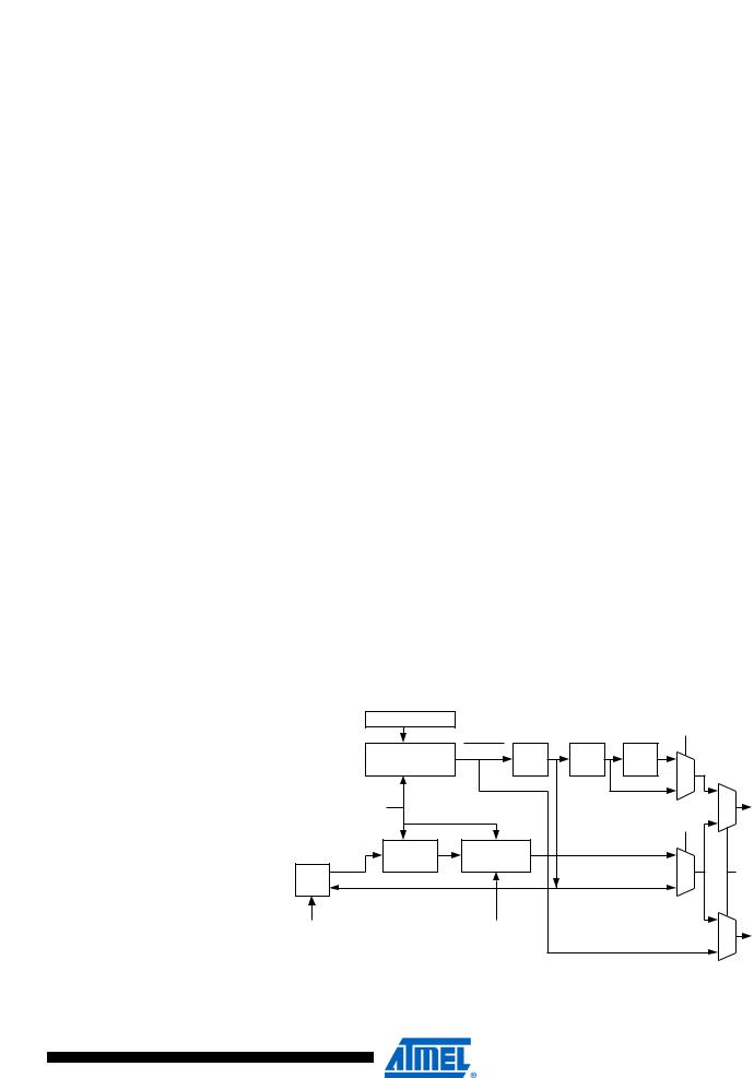
Clock Generation The clock generation logic generates the base clock for the transmitter and receiver. The USART supports four modes of clock operation: Normal Asynchronous, Double Speed Asynchronous, Master Synchronous, and Slave Synchronous mode. The UMSEL bit in USART Control and Status Register C (UCSRC) selects between asynchronous and synchronous operation. Double speed (Asynchronous mode only) is controlled by the U2X found in the UCSRA Register. When using Synchronous mode (UMSEL = 1), the Data Direction Register for the XCK pin (DDR_XCK) controls whether the clock source is internal (Master mode) or external (Slave mode). The XCK pin is only active when using Synchronous mode.
Figure 80 shows a block diagram of the clock generation logic.
Figure 80. Clock Generation Logic, Block Diagram |
|
|
|||
|
|
UBRR |
|
|
U2X |
|
|
|
fosc |
|
|
|
|
|
|
|
|
|
|
Prescaling |
UBRR+1 |
/ 4 |
/ 2 |
|
|
Down-Counter |
/ 2 |
||
|
|
|
|
0 |
|
|
|
|
|
|
1 |
|
OSC |
|
|
0 |
|
|
|
|
txclk |
||
|
|
|
|
|
1 |
|
|
|
|
|
DDR_XCK |
|
|
Sync |
Edge |
|
|
|
xcki |
Register |
Detector |
|
0 |
XCK |
xcko |
|
|
|
UMSEL |
Pin |
|
|
|
1 |
|
|
|
|
|
|
|
DDR_XCK |
|
|
UCPOL |
|
1 |
|
|
|
|
|
rxclk |
|
|
|
|
|
0 |
Signal description: |
|
|
|
|
|
172
2467X–AVR–06/11

 ATmega128
Internal Clock
Generation – The
Baud Rate Generator
txclk Transmitter clock. (Internal Signal) rxclk Receiver base clock. (Internal Signal)
xcki Input from XCK pin (internal Signal). Used for synchronous slave operation.
xcko Clock output to XCK pin (Internal Signal). Used for synchronous master operation.
fosc XTAL pin frequency (System Clock).
Internal clock generation is used for the asynchronous and the synchronous master modes of operation. The description in this section refers to Figure 80.
The USART Baud Rate Register (UBRR) and the down-counter connected to it function as a programmable prescaler or baud rate generator. The down-counter, running at system clock (fosc), is loaded with the UBRR value each time the counter has counted down to zero or when the UBRRL Register is written. A clock is generated each time the counter reaches zero. This clock is the baud rate generator clock output (= fosc/(UBRR+1)). The transmitter divides the baud rate generator clock output by 2, 8, or 16 depending on mode. The baud rate generator output is used directly by the receiver’s clock and data recovery units. However, the recovery units use a state machine that uses 2, 8, or 16 states depending on mode set by the state of the UMSEL, U2X and DDR_XCK bits.
Table 74 contains equations for calculating the baud rate (in bits per second) and for calculating the UBRR value for each mode of operation using an internally generated clock source.
Table 74. Equations for Calculating Baud Rate Register Setting
|
|
|
Equation for Calculating |
Equation for Calculating |
|
|||
|
Operating Mode |
Baud Rate(1) |
UBRR Value |
|
|
|||
|
Asynchronous Normal Mode |
BAUD = |
fOSC |
UBRR = |
fOSC |
|
|
|
|
(U2X = 0) |
|
16--------(--UBRR-------------------+-----1----) |
-----------------------16BAUD – 1 |
|
|||
|
Asynchronous Double Speed |
BAUD = |
fOSC |
UBRR = |
fOSC |
– 1 |
|
|
|
Mode (U2X = 1) |
8----(---UBRR-------------------+----1----)- |
8----BAUD---------------- |
|
||||
|
Synchronous Master Mode |
BAUD = |
fOSC |
UBRR = |
fOSC |
– 1 |
|
|
|
|
|
2----(---UBRR-------------------+----1----)- |
2----BAUD---------------- |
|
|||
|
Note: 1. |
The baud rate is defined to be the transfer rate in bit per second (bps). |
|
|
||||
|
BAUD |
Baud rate (in bits per second, bps) |
|
|
|
|
||
|
fOSC |
System Oscillator clock frequency |
|
|
|
|
|
|
|
UBRR |
Contents of the UBRRH and UBRRL Registers, (0 - 4095) |
|
|
|
|||
|
Some examples of UBRR values for some system clock frequencies are found in Table 82 (see |
|||||||
|
page 193). |
|
|
|
|
|
|
|
Double Speed |
The transfer rate can be doubled by setting the U2X bit in UCSRA. Setting this bit only has effect |
|||||||
Operation (U2X) |
for the asynchronous operation. Set this bit to zero when using synchronous operation. |
|||||||
Setting this bit will reduce the divisor of the baud rate divider from 16 to 8, effectively doubling the transfer rate for asynchronous communication. Note however that the receiver will in this case only use half the number of samples (reduced from 16 to 8) for data sampling and clock recovery, and therefore a more accurate baud rate setting and system clock are required when this mode is used. For the Transmitter, there are no downsides.
173
2467X–AVR–06/11
 ATmega128
External Clock |
External clocking is used by the synchronous slave modes of operation. The description in this |
|||||||||||||||||||
|
section refers to Figure 80 for details. |
|
|
|
|
|
|
|
|
|
|
|
|
|
||||||
|
External clock input from the XCK pin is sampled by a synchronization register to minimize the |
|||||||||||||||||||
|
chance of meta-stability. The output from the synchronization register must then pass through |
|||||||||||||||||||
|
an edge detector before it can be used by the transmitter and receiver. This process introduces |
|||||||||||||||||||
|
a two CPU clock period delay and therefore the maximum external XCK clock frequency is lim- |
|||||||||||||||||||
|
ited by the following equation: |
fOSC |
||||||||||||||||||
|
|
|
|
|
|
fXCK < |
||||||||||||||
|
|
|
|
|
|
----------- |
|
|
|
|
|
|
|
|
|
|
||||
|
|
|
|
|
|
4 |
|
|
|
|
|
|
|
|
|
|
|
|||
|
Note that fosc depends on the stability of the system clock source. It is therefore recommended to |
|||||||||||||||||||
|
add some margin to avoid possible loss of data due to frequency variations. |
|||||||||||||||||||
Synchronous Clock |
When Synchronous mode is used (UMSEL = 1), the XCK pin will be used as either clock input |
|||||||||||||||||||
Operation |
(slave) or clock output (master). The dependency between the clock edges and data sampling or |
|||||||||||||||||||
|
data change is the same. The basic principle is that data input (on RxD) is sampled at the oppo- |
|||||||||||||||||||
|
site XCK clock edge of the edge the data output (TxD) is changed. |
|||||||||||||||||||
|
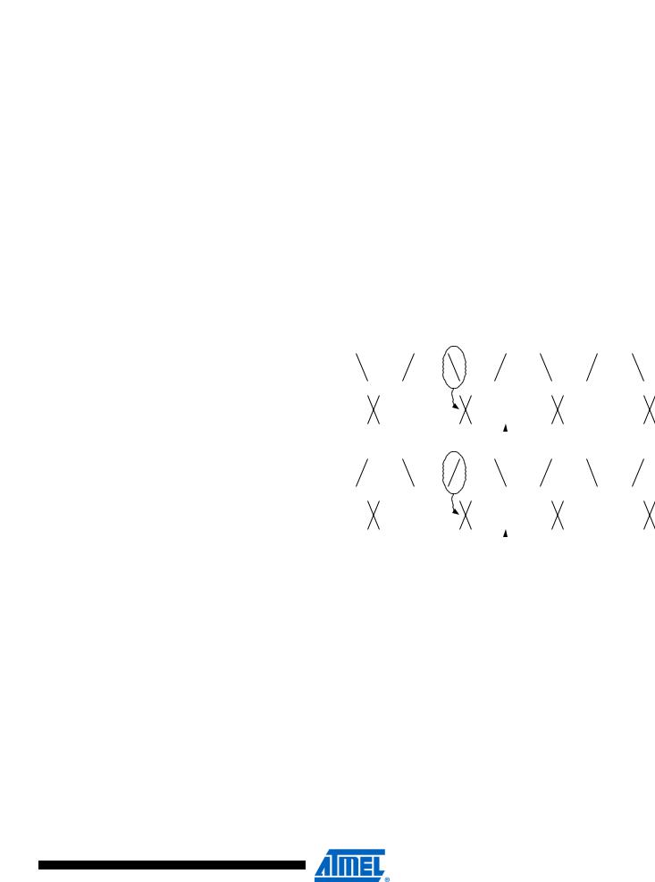
Figure 81. Synchronous Mode XCK Timing. |
|
|
|
|
|
|
|
|
|
|
|
|
|
||||||
|
UCPOL = 1 |
|
|
|
|
|
|
|
|
|
|
|
|
|
|
|
|
|
||
|
XCK |
|
|
|
|
|
|
|
|
|
|
|
|
|
||||||
|
|
|
|
|
|
|
|
|
|
|
|
|
|
|
|
|
|
|
|
|
|
|
|
|
|
|
|
|
|
|
|
|
|
|
|
|
|
|
|
|
|
|
|
RxD / TxD |
|
|
|
|
|
|
|
|
|
|
|
|
|
|||||
|
|
|
|
|
|
|
|
|
|
|
|
|
|
|
|
|
|
|
|
|
|
|
|
|
|
|
|
|
|
|
|
|
|
Sample |
|||||||
|
|
|
|
|
|
|
|
|
|
|
|
|||||||||
|
|
|
|
|
|
|
|
|
|
|
|
|
||||||||
|
|
|
|
|
|
|
|
|
|
|
|
|
|
|
|
|
|
|||
|
UCPOL = 0 |
XCK |
|
|
|
|
|
|
|
|
|
|
|
|
|
|||||
|
|
|
|
|
|
|
|
|
|
|
|
|
|
|
|
|
|
|||
|
|
|
|
|
|
|
|
|
|
|
|
|
|
|
|
|
|
|
|
|
|
|
RxD / TxD |
|
|
|
|
|
|
|
|
|
|
|
|
|
|||||
|
|
|
|
|
|
|
|
|
|
|
|
|
|
|
||||||
|
|
|
|
|
|
|
|
|
|
|
|
|
Sample |
|||||||
|
|
|
|
|
|
|
|
|
|
|
|
|
||||||||
|
|
|
|
|
|
|
|
|
|
|
|
|
||||||||
The UCPOL bit UCRSC selects which XCK clock edge is used for data sampling and which is used for data change. As Figure 81 shows, when UCPOL is zero the data will be changed at rising XCK edge and sampled at falling XCK edge. If UCPOL is set, the data will be changed at falling XCK edge and sampled at rising XCK edge.
174
2467X–AVR–06/11