

- •Features
- •Overview
- •Block Diagram
- •Pin Descriptions
- •Port A (PA7..PA0)
- •Port B (PB7..PB0)
- •Port C (PC7..PC0)
- •Port D (PD7..PD0)
- •Port E (PE7..PE0)
- •Port F (PF7..PF0)
- •Port G (PG4..PG0)
- •RESET
- •XTAL1
- •XTAL2
- •AVCC
- •AREF
- •Resources
- •Data Retention
- •Capacitive touch sensing
- •AVR CPU Core
- •Introduction
- •Status Register
- •Stack Pointer
- •I/O Memory
- •Overview
- •Timing
- •Using all Locations of External Memory Smaller than 64 Kbyte
- •Clock Systems and their Distribution
- •CPU Clock – clkCPU
- •I/O Clock – clkI/O
- •Flash Clock – clkFLASH
- •ADC Clock – clkADC
- •Clock Sources
- •Crystal Oscillator
- •External Clock
- •Idle Mode
- •Power-down Mode
- •Power-save Mode
- •Standby Mode
- •Analog Comparator
- •Brown-out Detector
- •Watchdog Timer
- •Port Pins
- •Resetting the AVR
- •Reset Sources
- •Power-on Reset
- •External Reset
- •Watchdog Reset
- •Watchdog Timer
- •Timed Sequences for Changing the Configuration of the Watchdog Timer
- •Safety Level 0
- •Safety Level 1
- •Safety Level 2
- •Interrupts
- •I/O Ports
- •Introduction
- •Configuring the Pin
- •Reading the Pin Value
- •Unconnected pins
- •Alternate Port Functions
- •Register Description for I/O Ports
- •8-bit Timer/Counter0 with PWM and Asynchronous Operation
- •Overview
- •Registers
- •Definitions
- •Counter Unit
- •Normal Mode
- •Fast PWM Mode
- •8-bit Timer/Counter Register Description
- •Overview
- •Registers
- •Definitions
- •Compatibility
- •Counter Unit
- •Input Capture Unit
- •Noise Canceler
- •Force Output Compare
- •Normal Mode
- •Fast PWM Mode
- •16-bit Timer/Counter Register Description
- •Internal Clock Source
- •Prescaler Reset
- •External Clock Source
- •8-bit Timer/Counter2 with PWM
- •Overview
- •Registers
- •Definitions
- •Counter Unit
- •Normal Mode
- •Fast PWM Mode
- •8-bit Timer/Counter Register Description
- •Output Compare Modulator (OCM1C2)
- •Overview
- •Description
- •Timing Example
- •Slave Mode
- •Master Mode
- •Data Modes
- •USART
- •Dual USART
- •Overview
- •AVR USART vs. AVR UART – Compatibility
- •Clock Generation
- •External Clock
- •Frame Formats
- •Parity Bit Calculation
- •Parity Generator
- •Receiver Error Flags
- •Parity Checker
- •Disabling the Receiver
- •Using MPCM
- •Features
- •TWI Terminology
- •Transferring Bits
- •Address Packet Format
- •Data Packet Format
- •Overview of the TWI Module
- •Scl and SDA Pins
- •Bus Interface Unit
- •Address Match Unit
- •Control Unit
- •Using the TWI
- •Master Receiver Mode
- •Slave Receiver Mode
- •Miscellaneous States
- •Analog Comparator
- •Analog to Digital Converter
- •Features
- •Operation
- •Changing Channel or Reference Selection
- •ADC Input Channels
- •Analog Input Circuitry
- •Features
- •Overview
- •TAP Controller
- •PRIVATE0; $8
- •PRIVATE1; $9
- •PRIVATE2; $A
- •PRIVATE3; $B
- •Bibliography
- •Features
- •System Overview
- •Data Registers
- •Bypass Register
- •Reset Register
- •EXTEST; $0
- •IDCODE; $1
- •AVR_RESET; $C
- •BYPASS; $F
- •Scanning the ADC
- •ATmega128 Boundary-scan Order
- •Application Section
- •Programming Time for Flash when Using SPM
- •Simple Assembly Code Example for a Boot Loader
- •Fuse Bits
- •Latching of Fuses
- •Signature Bytes
- •Calibration Byte
- •Signal Names
- •Chip Erase
- •Reading the Flash
- •Reading the EEPROM
- •Data Polling Flash
- •Data Polling EEPROM
- •AVR_RESET ($C)
- •PROG_ENABLE ($4)
- •Data Registers
- •Reset Register
- •Programming Enable Register
- •Programming Command Register
- •Virtual Flash Page Read Register
- •Performing Chip Erase
- •Reading the Flash
- •Reading the EEPROM
- •Electrical Characteristics
- •Absolute Maximum Ratings*
- •DC Characteristics
- •Speed Grades
- •External Clock Drive Waveforms
- •External Clock Drive
- •Two-wire Serial Interface Characteristics
- •ADC Characteristics
- •External Data Memory Timing
- •Idle Supply Current
- •Pin Pull-up
- •Pin Driver Strength
- •Register Summary
- •Instruction Set Summary
- •Ordering Information
- •Packaging Information
- •Errata
- •ATmega128 Rev. F to M

 ATmega128
3.The SPI Serial Programming instructions will not work if the communication is out of synchronization. When in sync. the second byte ($53), will echo back when issuing the third byte of the Programming Enable instruction. Whether the echo is correct or not, all FOUR bytes of the instruction must be transmitted. If the $53 did not echo back, give RESET a positive pulse and issue a new Programming Enable command.
4.The Flash is programmed one page at a time. The page size is found in Table 124 on page 291. The memory page is loaded one byte at a time by supplying the 7 LSB of the address and data together with the Load Program Memory Page instruction. To ensure correct loading of the page, the data low byte must be loaded before data high byte is applied for given address. The Program Memory Page is stored by loading the Write Program Memory Page instruction with the 9MSB of the address. If polling is not used, the user must wait at least tWD_FLASH before issuing the next page. (See Table 128).
Note: If other commands than polling (read) are applied before any write operation (Flash, EEPROM, Lock bits, Fuses) is completed, may result in incorrect programming.
5.The EEPROM array is programmed one byte at a time by supplying the address and data together with the appropriate Write instruction. An EEPROM memory location is first automatically erased before new data is written. If polling is not used, the user must wait
at least tWD_EEPROM before issuing the next byte. (See Table 128). In a chip erased device, no $FFs in the data file(s) need to be programmed.
6.Any memory location can be verified by using the Read instruction which returns the content at the selected address at serial output MISO.
7.At the end of the programming session, RESET can be set high to commence normal operation.
8.Power-off sequence (if needed): Set RESET to “1”.
Turn VCC power off.
Data Polling Flash When a page is being programmed into the Flash, reading an address location within the page being programmed will give the value $FF. At the time the device is ready for a new page, the programmed value will read correctly. This is used to determine when the next page can be written. Note that the entire page is written simultaneously and any address within the page can be used for polling. Data polling of the Flash will not work for the value $FF, so when programming
this value, the user will have to wait for at least tWD_FLASH before programming the next page. As a chip-erased device contains $FF in all locations, programming of addresses that are meant to
contain $FF, can be skipped. See Table 128 for tWD_FLASH value
Data Polling EEPROM When a new byte has been written and is being programmed into EEPROM, reading the address location being programmed will give the value $FF. At the time the device is ready for a new byte, the programmed value will read correctly. This is used to determine when the next byte can be written. This will not work for the value $FF, but the user should have the following in mind: As a chip-erased device contains $FF in all locations, programming of addresses that are meant to contain $FF, can be skipped. This does not apply if the EEPROM is re-programmed without chip-erasing the device. In this case, data polling cannot be used for the value $FF, and the user will have to wait at least t before programming the next byte. See Table 128 for tWD_EEPROM value.
302
2467X–AVR–06/11
 ATmega128
Table 128. Minimum Wait Delay before Writing the Next Flash or EEPROM Location, VCC = 5V ±10%
Symbol |
Minimum Wait Delay |
|
|
tWD_FUSE |
4.5ms |
tWD_FLASH |
5ms |
tWD_EEPROM |
10ms |
tWD_ERASE |
10ms |
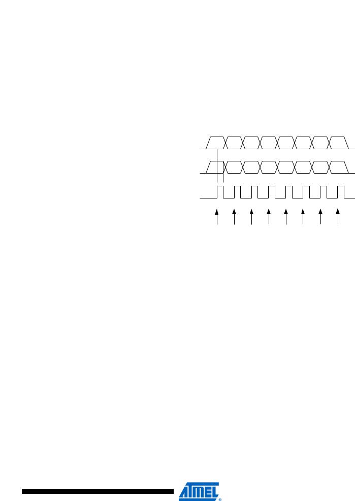
Figure 145. .SPI Serial Programming Waveforms
SERIAL DATA INPUT |
MSB |
LSB |
(MOSI) |
|
|
SERIAL DATA OUTPUT |
MSB |
LSB |
(MISO) |
|
|
SERIAL CLOCK INPUT |
|
|
(SCK) |
|
|
SAMPLE |
|
|
303
2467X–AVR–06/11

 ATmega128
Table 129. SPI Serial Programming Instruction Set
|
|
Instruction Format |
|
|
|
|
|
|
|
|
|
|
|
||
Instruction |
Byte 1 |
Byte 2 |
Byte 3 |
Byte 4 |
Operation |
||
|
|
|
|
|
|
|
|
Programming Enable |
1010 1100 |
0101 0011 |
xxxx xxxx |
xxxx xxxx |
Enable SPI Serial Programming after |
|
|
RESET |
|||||||
|
|
|
|
|
goes low. |
||
|
|
|
|
|
|
||
Chip Erase |
1010 1100 |
100x xxxx |
xxxx xxxx |
xxxx xxxx |
Chip Erase EEPROM and Flash. |
||
|
|
|
|
|
|
||
Read Program |
0010 H000 |
aaaa aaaa |
bbbb bbbb |
oooo oooo |
Read H (high or low) data o from Program |
||
Memory |
|
|
|
|
memory at word address a:b. |
||
|
|
|
|
|
|
||
Load Program |
0100 H000 |
xxxx xxxx |
xbbb bbbb |
iiii iiii |
Write H (high or low) data i to Program |
||
Memory Page |
|
|
|
|
Memory page at word address b. Data low |
||
|
|
|
|
|
byte must be loaded before data high byte is |
||
|
|
|
|
|
applied within the same address. |
||
|
|
|
|
|
|
|
|
Write Program |
0100 1100 |
aaaa aaaa |
bxxx xxxx |
xxxx xxxx |
|
|
|
Memory Page |
|
|
|
|
Write Program Memory Page at address a:b. |
||
|
|
|
|
|
|
||
Read EEPROM |
1010 0000 |
xxxx aaaa |
bbbb bbbb |
oooo oooo |
Read data o from EEPROM memory at |
||
Memory |
|
|
|
|
address a:b. |
||
|
|
|
|
|
|
||
Write EEPROM |
1100 0000 |
xxxx aaaa |
bbbb bbbb |
iiii iiii |
Write data i to EEPROM memory at address |
||
Memory |
|
|
|
|
a:b. |
||
|
|
|
|
|
|
||
Read Lock bits |
0101 1000 |
0000 0000 |
xxxx xxxx |
xxoo oooo |
Read Lock bits. “0” = programmed, “1” = |
||
|
|
|
|
|
unprogrammed. See Table 115 on page |
||
|
|
|
|
|
286 for details. |
||
|
|
|
|
|
|
||
Write Lock bits |
1010 1100 |
111x xxxx |
xxxx xxxx |
11ii iiii |
Write Lock bits. Set bits = “0” to program Lock |
||
|
|
|
|
|
bits. See Table 115 on page 286 for details. |
||
|
|
|
|
|
|
||
Read Signature Byte |
0011 0000 |
xxxx xxxx |
xxxx xxbb |
oooo oooo |
Read Signature Byte o at address b. |
||
|
|
|
|
|
|
||
Write Fuse bits |
1010 1100 |
1010 0000 |
xxxx xxxx |
iiii iiii |
Set bits = “0” to program, “1” to unprogram. |
||
|
|
|
|
|
See Table 119 on page 288 for details. |
||
|
|
|
|
|
|
||
Write Fuse High Bits |
1010 1100 |
1010 1000 |
xxxx xxxx |
iiii iiii |
Set bits = “0” to program, “1” to unprogram. |
||
|
|
|
|
|
See Table 118 on page 288 for details. |
||
|
|
|
|
|
|
||
Write Extended Fuse |
1010 1100 |
1010 0100 |
xxxx xxxx |
xxxx xxii |
Set bits = “0” to program, “1” to unprogram. |
||
bits |
|
|
|
|
See Table 119 on page 288 for details. |
||
|
|
|
|
|
|
||
Read Fuse bits |
0101 0000 |
0000 0000 |
xxxx xxxx |
oooo oooo |
Read Fuse bits. “0” = programmed, “1” = |
||
|
|
|
|
|
unprogrammed. See Table 119 on page |
||
|
|
|
|
|
288 for details. |
||
|
|
|
|
|
|
||
Read Extendend |
0101 0000 |
0000 1000 |
xxxx xxxx |
oooo oooo |
Read Extended Fuse bits. “0” = pro-grammed, |
||
Fuse bits |
|
|
|
|
“1” = unprogrammed. See Table 119 on |
||
|
|
|
|
|
page 288 for details. |
||
|
|
|
|
|
|
||
Read Fuse High Bits |
0101 1000 |
0000 1000 |
xxxx xxxx |
oooo oooo |
Read Fuse high bits. “0” = pro-grammed, “1” = |
||
|
|
|
|
|
unprogrammed. See Table 118 on page |
||
|
|
|
|
|
288 for details. |
||
|
|
|
|
|
|
||
Read Calibration Byte |
0011 1000 |
xxxx xxxx |
0000 00bb |
oooo oooo |
Read Calibration Byte o at address b. |
||
|
|
|
|
|
|
|
|
Note: a = address high bits b = address low bits
H = 0 - Low byte, 1 - High Byte o = data out
i = data in
x = don’t care
304
2467X–AVR–06/11

 ATmega128
SPI Serial |
For characteristics of the SPI module, see “SPI Timing Characteristics” on page 323. |
Programming |
|
Characteristics |
|
Programming Via |
Programming through the JTAG interface requires control of the four JTAG specific pins: TCK, |
the JTAG Interface |
TMS, TDI, and TDO. Control of the Reset and clock pins is not required. |
|
To be able to use the JTAG interface, the JTAGEN fuse must be programmed. The device is |
|
default shipped with the Fuse programmed. In addition, the JTD bit in MCUCSR must be |
|
cleared. Alternatively, if the JTD bit is set, the external reset can be forced low. Then, the JTD bit |
|
will be cleared after two chip clocks, and the JTAG pins are available for programming. This pro- |
|
vides a means of using the JTAG pins as normal port pins in running mode while still allowing In- |
|
System Programming via the JTAG interface. Note that this technique can not be used when |
|
using the JTAG pins for Boundary-scan or On-chip Debug. In these cases the JTAG pins must |
|
be dedicated for this purpose. |
|
As a definition in this data sheet, the LSB is shifted in and out first of all Shift Registers. |
Programming Specific |
The instruction register is 4-bit wide, supporting up to 16 instructions. The JTAG instructions |
JTAG Instructions |
useful for Programming are listed below. |
|
The OPCODE for each instruction is shown behind the instruction name in hex format. The text |
|
describes which data register is selected as path between TDI and TDO for each instruction. |
|
The Run-Test/Idle state of the TAP controller is used to generate internal clocks. It can also be |
|
used as an idle state between JTAG sequences. The state machine sequence for changing the |
|
instruction word is shown in Figure 146. |
305
2467X–AVR–06/11