

- •Single-User License Agreement
- •Chapter 1: Design Goals of USB
- •Chapter 2: The Big Picture
- •Chapter 3: Cables and Connectors
- •Chapter 4: USB Cable Power Distribution
- •Chapter 5: LS/FS Signaling Environment
- •Chapter 6: LS/FS Transfer Types & Scheduling
- •Chapter 7: Packets & Transactions
- •Chapter 8: Error Recovery
- •Chapter 9: USB Power Conservation
- •Chapter 10: Overview of HS Device Operation
- •Chapter 11: The High-Speed Signaling Environment
- •Chapter 12: HS Transfers, Transactions, & Scheduling
- •Chapter 13: HS Error Detection and Handling
- •Chapter 14: HS Suspend and Resume
- •Chapter 15: HS Hub Overview
- •Chapter 16: 2.0 Hubs During HS Transactions
- •Chapter 17: 2.0 Hubs During LS/FS Transactions
- •Chapter 18: Configuration Process
- •Chapter 19: USB Device Configuration
- •Chapter 20: Hub Configuration
- •Chapter 21: Device Classes
- •Chapter 22: Overview of USB Host Software
- •Appendix A: Standard Device Requests
- •Appendix B: Hub Requests
- •Appendix C: Universal Host Controller
- •Appendix D: Open Host Controller
- •About This Book
- •The MindShare Architecture Series
- •Cautionary Note
- •Specifications This Book is Based On
- •Organization of This Book
- •Part One: Overview of USB 2.0
- •Part Two: Low- & Full-Speed Device Operation
- •Part III: High-Speed Device Operation
- •Part IV: USB 2.0 Hub Operation with LS/FS/HS Devices
- •Part VI: USB Software Overview
- •Appendices
- •Who Should Read this Book
- •Prerequisite Knowledge
- •Documentation Conventions
- •Hexadecimal Notation
- •Binary Notation
- •Decimal Notation
- •Bits Versus Byte Notation
- •Identification of Bit Fields (logical groups of bits or signals)
- •Visit Our Web Page
- •We Want Your Feedback
- •Shortcomings of the Original PC I/O Paradigm
- •Limited System Resources
- •Interrupts
- •I/O Addresses
- •Non-shareable Interfaces
- •End User Concerns
- •Cable Crazed
- •Installation and Configuration of Expansion Cards
- •No Hot Attachment of Peripherals
- •Cost
- •The USB Paradigm
- •Enhanced System Performance
- •Hot Plug and Play Support
- •Expandability
- •Legacy Hardware/Software Support
- •Low Cost
- •Summary of Key USB Features
- •How to Get the USB Specifications
- •2 The Big Picture
- •Overview
- •USB 1.x Systems and Devices
- •Low-Speed and Full-Speed Devices
- •How Transactions Are Generated
- •What the Descriptors Contain
- •How the Transfer Descriptors Are Fetched
- •Frame Generation
- •Sharing the Bus
- •Bandwidth Consideration Summary
- •2.0 Systems and Devices
- •Low-Speed and Full-Speed Devices in a 2.0 System
- •Example 2.0 Host Controller Support for LS/FS Devices
- •High-Speed Devices in a 2.0 System
- •High-Speed Devices Attached to 1.x Ports
- •High-Speed Transactions and Microframe Generation
- •High-Speed Bandwidth Summary
- •The Players
- •USB Client Drivers
- •USB Bus Driver
- •USB Host Controller Driver
- •USB Host Controller/Root Hub
- •The Host Controller
- •The Root Hub
- •USB Hubs
- •Hub Controller
- •Hub Repeater
- •Hub’s Role in Configuration
- •USB Devices
- •High-Speed Devices
- •Full-Speed Devices
- •Low-Speed Devices
- •USB Communications Model
- •Communications Flow
- •Transfers, IRPs, Frames, and Packets
- •Transfers
- •The USB Driver, IRPs, and Frames
- •The Host Controller Driver and Transactions
- •The Host Controller and Packets
- •Device Framework (how devices present themselves to software)
- •Device Descriptors
- •Device Framework
- •USB Bus Interface Layer
- •USB Device Layer
- •Function Layer
- •USB Peripheral Connection
- •Full-Speed Hubs
- •High-Speed Hubs
- •High-Speed Devices
- •Topology
- •The Connectors
- •Series A Connectors
- •Series B Connectors
- •Cables
- •Low-Speed Cables
- •Cable Power
- •Electrical and Mechanical Specifications
- •USB Power
- •Hubs
- •Current Budget
- •Over-Current Protection
- •Voltage Drop Budget
- •Power Switching
- •Bus-Powered Hubs
- •Power During Hub Configuration
- •Bus-Powered Hub Attached to 500ma Port
- •Bus-Powered Hub Attached to 100ma Port
- •Bus-Powered Hub Attached to Port with >100ma but <500ma
- •Current Limiting
- •Bus-Powered Devices
- •Low-Power Devices
- •High-Power Devices
- •Power During Configuration
- •Insufficient Port Power
- •Self-Powered Hubs
- •Power During Configuration
- •Locally Powered Bus Interface
- •Hybrid Powered Device
- •Current Limiting
- •Self-Powered Devices
- •Power During Configuration
- •Locally Powered Bus Interface
- •Hybrid Powered Device
- •Overview
- •Detecting Device Attachment and Speed Detect
- •Full-Speed Device Connect
- •Low-Speed Device Connect
- •Detecting Device Disconnect
- •Bus Idle
- •Device RESET
- •Differential Signaling
- •Differential Drivers
- •Full-Speed Drivers
- •Low-Speed Drivers
- •Hub Driver Characteristics
- •Differential Receivers
- •Start of Packet (SOP)
- •End of Packet (EOP)
- •Single-Ended Receivers
- •NRZI Encoding
- •Bit Stuffing
- •Summary of USB Signaling States
- •Overview
- •Client Initiates Transfer
- •Communications Pipes
- •Communication Initiated by I/O Request Packets
- •Frame-Based Transfers
- •Transfer Types
- •Isochronous Transfers
- •Direction of Transfers
- •Service Period
- •Bandwidth Allocation
- •Error Recovery
- •Establishing Synchronous Connections
- •The Problem with Isochronous Transfers
- •The Feedback/Feed Forwarding Solution
- •Synchronization Types
- •Source/Sink Combinations and Synchronization Methods
- •How Endpoints Report Their Synchronization Capabilities
- •Feedback Data
- •Association Between Data Endpoint and Feedback Endpoint
- •Interrupt Transfers
- •Service Period
- •Bus Bandwidth Allocation
- •Error Recovery
- •Control Transfers
- •Bus Bandwidth Allocation
- •Error Recovery
- •Bulk Transfers
- •Bus Bandwidth Allocation
- •Error Recovery
- •Overview
- •Packets — The Basic Building Blocks of USB Transactions
- •Synchronization Sequence
- •Packet Identifier
- •Packet-Specific Information
- •Cyclic Redundancy Checking (CRC)
- •End of Packet (EOP)
- •Token Packets
- •SOF Packet
- •IN Packet
- •OUT Packet
- •SETUP Packet
- •Data Packets — DATA0 and Data1
- •Handshake Packets
- •Preamble Packet
- •Transactions
- •IN Transactions
- •IN Transaction Without Errors
- •IN Transaction with Errors
- •IN Transaction with No Interrupt Pending/Target Busy
- •IN Transaction with Target Stalled
- •IN Transaction During Isochronous Transfer
- •OUT Transactions
- •OUT Transaction Without Data Packet Errors
- •OUT Transaction with Errors
- •OUT Transaction — Target Unable to Accept Data
- •OUT Transaction With Target Stalled
- •OUT Transaction During Isochronous Transfer
- •Setup Transactions/Control Transfers
- •Two Stage Control Transfer
- •Three Stage Control Transfer with IN Data Stage
- •Three Stage Control Transfer with OUT Data Stage
- •Control Transfers With Errors
- •8 Error Recovery
- •Overview
- •Packet Errors
- •PID Checks
- •CRC Errors
- •Bit Stuff Errors
- •Packet-Related Error Handling
- •Token Packet Errors
- •Data Packet Errors
- •Handshake Packet Errors
- •Bus Time-Out
- •False EOPs
- •False EOP During Host Transmission
- •False EOP During Target Transmission
- •Data Toggle Errors
- •Data Toggle Procedure Without Errors
- •Data Toggle during OUT Transactions
- •Data Toggle During IN Transactions
- •Data Toggle Procedure with Data Packet Errors
- •Data Toggle and Data Packet Errors — OUT Transactions
- •Data Toggle and Data Packet Errors — IN Transactions
- •Data Toggle With Handshake Packet Error — IN Transaction
- •Special Case: Data Toggle During Control Transfer
- •Babbling Devices
- •Loss of Activity (LOA)
- •Babble/LOA Detection and Recovery
- •Frame Timer
- •Host to Hub Skew
- •Hub Repeater State Machine
- •Isochronous Transfers (Delivery Not Guaranteed)
- •Interrupt Transfer Error Recovery
- •Bulk Transfer Error Recovery
- •Control Transfer Error Recovery
- •Power Conservation — Suspend
- •Device Response to Suspend
- •Hub Response to Suspend
- •Global Suspend
- •Initiating Global Suspend
- •Resume from Global Suspend
- •Resume Initiated by Host
- •Remote Wakeup from Device
- •Remote Wakeup via Hub Port Event
- •Selective Suspend
- •Initiating Selective Suspend
- •Resume from Selective Suspend
- •Host Initiated Selective Resume
- •Selective Wakeup from Device
- •Selective Suspend When Hub is Suspended
- •Device Signals Resume
- •Port Receives Connect or Disconnect
- •Selective Suspend Followed by Global Suspend
- •Resume via Reset
- •Hub Frame Timer After Wakeup
- •Overview
- •New High-Speed Device Features
- •1.x USB Device Support
- •The 2.0 Host Controller
- •Overview
- •Detecting High-Speed Device Attachment
- •Initial Device Detection
- •Device Reset and the Chirp Sequence
- •High-Speed Interfaces Idled
- •High-Speed Differential Signaling
- •Impedance Matching
- •High-Speed Driver Characteristics
- •High-Speed Idle
- •High-Speed Differential Receivers
- •High-Speed Driver/Receiver Compliance Testing
- •Activating Test Mode
- •The Test Setup
- •Eye Pattern Tests
- •High-Speed Start of Packet & Synchronization Sequence
- •High-Speed End of Packet (EOP)
- •Detection of High-Speed Device Removal
- •High-Speed RESET and Suspend
- •Signaling RESET
- •Signaling Suspend
- •Differentiating Between RESET and Suspend
- •Overview
- •High-Speed Transaction Scheduling
- •Microframes
- •Theoretical HS Bandwidth
- •Periodic Transfers
- •High-Speed Isochronous Transfers
- •Maximum Packet Size
- •Isochronous Bandwidth/Performance
- •Isochronous Transaction Errors
- •High-Speed Interrupt Transfers
- •Maximum Packet Size
- •Interrupt Bandwidth
- •Interrupt Transaction Errors
- •High-Bandwidth Transactions
- •Detecting High-Bandwidth Endpoints and Packet Size
- •Isochronous High-Bandwidth Scheduling and Protocol
- •High Bandwidth Interrupt Transactions
- •High Bandwidth Throughput
- •Non-Periodic Transfers
- •High-Speed Bulk Transfers
- •Maximum Packet Size
- •Bulk Bandwidth
- •Bulk Transactions Errors
- •High-Speed Control Transfers
- •High-Speed Control Bandwidth
- •Ping Transactions
- •The Problem
- •The Solution
- •The Ping Protocol
- •Overview
- •High-Speed Bus Time-out
- •False EOP
- •HS Babbling Device Detection
- •Overview
- •Entering Device Suspend
- •Device Resume
- •15 HS Hub Overview
- •Overview
- •USB 2.0 Hub Attached to High-Speed Port
- •High-Speed Transactions
- •USB 2.0 Hub Attached to Full-Speed Port
- •Overview
- •High-Speed Hub Repeater
- •Receiver Squelch
- •Re-clocking the Packet
- •Port Selector State Machine
- •Elasticity Buffer
- •The Repeater State Machine
- •Overview
- •The Structure of Split Transactions
- •Isochronous Split Transaction Examples
- •Example Split Isochronous OUT Transaction
- •Example Split Isochronous IN Transaction
- •Example Split Transactions with Data Verification
- •Split OUT Sequence
- •Split IN Sequence
- •The Split Token Packet
- •The Transaction Translator
- •The Major Elements of the Transaction Translator
- •High-Speed Handler
- •Periodic Transfer Start-Split Buffer
- •Periodic Complete-Split Buffer
- •Bulk/Control Buffers
- •Low-Speed/Full-Speed Handler
- •Split Transaction Scheduling
- •Split Transaction Scheduling Example
- •SOF Packets
- •Host Delivers Isochronous Start Split
- •Host Delivers Interrupt Start Split
- •Host Issues Complete-Split to Fetch Isochronous IN Data
- •Host Fetches Interrupt OUT Completion Status
- •Host Continues to Fetch Isochronous IN Data
- •Transaction End
- •High-Speed Scheduling Can Include Other Transactions
- •Single versus Multiple Transaction Translators
- •Periodic Split Transactions
- •Periodic Split Transaction Pipeline
- •High Speed Handler Receives Start Split
- •Start-Split Buffer
- •Low-Speed/Full-Speed Handler
- •Complete-Split Buffer
- •Isochronous OUT Split Transaction Sequence
- •Isochronous OUT Start Split
- •Handling CRC16 During Split Isochronous OUT Transactions
- •Isochronous IN Split Transaction Sequence
- •Isochronous IN Start Split
- •Isochronous IN Complete Split
- •Handling CRC16 During Split Isochronous IN Transactions
- •Interrupt Split OUT Transaction Sequence
- •Interrupt OUT Start Split Sequence
- •Interrupt OUT Complete Split Sequence
- •Interrupt IN Split Transaction Sequence
- •Interrupt IN Start Split Sequence
- •Interrupt IN Complete Split Sequence
- •Handling CRC16 During Split Interrupt IN Transactions
- •Non Periodic Split Transactions
- •Non-Periodic Split Transaction Pipeline
- •High Speed Handler
- •Non-periodic Buffers
- •Low-/Full-Speed Handler
- •Bulk/Control Split OUT Transaction Sequence
- •Bulk/Control OUT Start Split Sequence
- •Bulk/Control OUT Complete Split Sequence
- •Bulk/Control Split IN Transaction Sequence
- •Bulk/Control IN Start Split Sequence
- •Bulk/Control IN Complete Split Sequence
- •Overview
- •The Configuration Software Elements
- •USB Host Controller Driver
- •Configuration Software
- •Default Control Pipe
- •Resource Management
- •Device Client Software
- •Root Hub Configuration
- •Each Device Is Isolated for Configuration
- •Reset Forces Device to Default Address (zero)
- •Host Assigns a Unique Device Address
- •Host Software Verifies Configuration
- •Power Requirements
- •Bus Bandwidth
- •Configuration Value Is Assigned
- •Client Software Is Notified
- •Overview
- •Summary of Configuration Process
- •How Software Detects Device Attachment & Speed
- •Polling the Status Change Endpoint
- •Getting Port Status
- •Resetting the Port
- •Reading and Interpreting the USB Descriptors
- •The Standard Descriptors
- •How Software Accesses the Descriptors
- •Device Descriptor
- •Class Code Field
- •Maximum Packet Size Zero
- •Manufacturer, Product, Serial Number
- •Number of Configurations
- •Device Qualifier Descriptor
- •Configuration Descriptors
- •Number of Interfaces
- •Configuration Value
- •Attributes and Maximum Power
- •Other Speed Configuration Descriptor
- •Interface Descriptors
- •Interface Number and Alternate Setting
- •Number of Endpoints
- •Interface Class and Subclass
- •Protocol
- •Endpoint Descriptors
- •Device States
- •Attached State
- •Powered State
- •Default State
- •Addressed State
- •Configured State
- •Suspend State
- •Client Software Configuration
- •Configuring the Hub
- •The Default Pipe
- •The Status Change Pipe
- •Reading the Hub’s Descriptors
- •1.x Hub Descriptors
- •Hub’s Standard Device Descriptor
- •Hub Configuration Descriptor
- •Number of Interfaces
- •Configuration Value
- •Maximum Bus Power Consumed
- •Hub Interface Descriptor
- •Status Endpoint Descriptor
- •Status Change Endpoint Address/Transfer Direction
- •Transfer Type
- •Maximum Data Packet Size
- •Polling Interval
- •Hub Class Descriptor
- •Power Switching Mode Implemented
- •Compound Device or Hub Only
- •Over-Current Protection Mode
- •Power On to Power Good Delay
- •Maximum Bus Current for Hub Controller
- •Device Removable/Non-removable
- •Port Power Mask
- •High-Speed Capable Hub Descriptors
- •Descriptors When Hub Is Operating at Full Speed
- •The 2.0 Hub’s Class-Specific Descriptor
- •Powering the Hub
- •Checking Hub Status
- •Detecting Hub Status Changes
- •Reading the Hub Status Field
- •Reading Port Status
- •Enabling the Device
- •Summary of Hub Port States
- •21 Device Classes
- •Overview
- •Device Classes
- •Audio Device Class
- •Standard Audio Interface Requirements
- •Synchronization Types
- •Audio Class-Specific Descriptors
- •Audio Class-Specific Requests
- •Communications Device Class
- •Communications Device Interfaces
- •Communications Class-Specific Descriptors
- •Communications Class-Specific Requests
- •Display Device Class
- •The Standard Display Device Class Interface
- •Display Device-Specific Descriptors
- •Device-Specific Requests
- •Mass Storage Device Class
- •Standard Mass Storage Interface
- •Control Endpoint
- •Bulk Transfer Endpoints
- •Interrupt Endpoint
- •General Mass Storage Subclass
- •CD-ROM Subclass
- •Tape Subclass
- •Solid State Subclass
- •USB Software
- •Function Layer
- •Device Layer
- •Interface Layer
- •The Software Components
- •USB Driver (USBD)
- •Configuration Management
- •USB Elements Requiring Configuration
- •Allocating USB Resources
- •Verifying Power
- •Tracking and Allocating Bus Bandwidth
- •Bus Bandwidth Reclamation
- •Data Transfer Management
- •Providing Client Services (The USB Driver Interface)
- •Pipe Mechanisms
- •Client Pipe Requirements
- •Command Mechanisms
- •Appendix
- •Overview
- •Standard Device Requests
- •Set/Clear Feature
- •Device Remote Wakeup
- •Endpoint Stall
- •Set/Get Configuration
- •Set/Get Descriptor
- •Set/Get Interface
- •Get Status
- •Device Status
- •Self-Powered Bit
- •Remote Wakeup Bit
- •Port Test Bit
- •Endpoint Status
- •Sync Frame
- •Device Tests
- •High-speed Driver/Receiver Compliance Testing
- •Activating Test Mode
- •Overview
- •Hub Request Types
- •Standard Requests and Hub Response
- •Hub Class Requests
- •Get/Set Descriptor Request
- •Get Hub Status Request
- •Hub Status Fields
- •Local Power Status
- •Over-Current Indicator
- •Hub State Change Fields
- •Local Power Status Change
- •Over-Current Indicator Change
- •Set/Clear Hub Feature Request
- •Hub Local Power Change Request
- •Hub Over-Current Change Request
- •Get Port Status Request
- •Port Status Fields
- •Current Connect Status Field
- •Port Enabled/Disabled
- •Suspend
- •Over-Current Indicator
- •Reset
- •Port Power
- •Low-Speed Device Attached
- •High-Speed Device Attached
- •Port Test
- •Port Indicator Control
- •Port Change Fields
- •Current Status Change
- •Port Enable/Disable Change
- •Suspend Change (Resume Complete)
- •Over-Current Indicator Change
- •Reset Complete
- •Set/Clear Port Feature
- •Port Test Modes
- •Get Bus State
- •Overview
- •Universal Host Controller Transaction Scheduling
- •Universal Host Controller Frame List Access
- •UHC Transfer Scheduling Mechanism
- •Bus Bandwidth Reclamation
- •Transfer Descriptors
- •Queue Heads
- •UHC Control Registers
- •Overview
- •Open Host Controller Transfer Scheduling
- •The Open Host Controller Transfer Mechanism
- •The ED and TD List Structure
- •Interrupt and Isochronous Transfer Processing
- •Control and Bulk Transfer Processing
- •The Done Queue
- •Interrupt Transfer Scheduling
- •Endpoint Descriptors
- •Transfer Descriptors
- •General Transfer Descriptor
- •Isochronous Transfer Descriptor
- •The Open Host Controller Registers
- •Index
USB System Architecture
Differential Drivers
USB differential drivers can be designed for low-speed, full-speed, or both lowand full-speed operation. A differential driver employs inverting and noninverting buffers. The input signal is applied to both buffers, yielding two outputs (D+ and D-).
Full-Speed Drivers
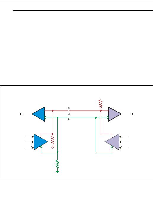
Full-speed drivers signal across the fully rated cable (shielded/twisted pair). A full-speed cable has a characteristic impedance of 90Ω and a maximum length of 5 meters. Figure 5-12 illustrates a FS connection and the differential drivers and receivers.
Figure 5-12: Full-Speed Differential Drivers and Receivers
8SVWUHDP |
|
&DEOH |
'RZQVWUHDP |
|
|
3RUW |
|
|
3RUW |
|
|
|
6HJPHQW |
'FF |
|
||
+XE |
|
< |
.: |
|
|
|
|
' |
|
|
|
|
|
|
|
|
|
'LIIHUHQWLDO 5HFHLYH |
|
U |
|
'LIIHUHQWLDO 5HFHLYH |
|
|
|
|
|
||
;PW 'DW |
D |
|
|
;PW 'DW |
D |
6(2 |
|
|
|
6(2 |
|
2( |
|
|
|
2( |
|
'LIIHUHQWLDO 'ULYH U |
|
|
|
'LIIHUHQWLDO 'ULYH U |
|
|
|
|
|
||
|
|
.: |
|
|
|
The output impedance of the driver must be in the range of 28 to 44 ohms. This impedance is typically achieved with a CMOS buffer implementation by adding series resistors as illustrated in Figure 5-13 on page 107. The specification defines the conditions under which the output impedance is tested and measured.
106

Chapter 5: LS/FS Signaling Environment
Figure 5-13: CMOS Buffer with Series Resistors Achieve Specified Output Impedance
|
|
|
27 |
Ω |
|||||
|
|
|
|
|
|
|
|
|
D+ (28Ω to 44Ω Equiv. I |
|
|
|
|
|
|
|
|
||
Data |
|
OE |
|
Identical CMOS Buffe |
|
|
rs |
||
|
|
(with output imped, = 3 |
Ω to 15Ω |
||||||
|
|
||||||||
D+ (28Ω to 44Ω Equiv. I
27Ω
Slew rate control is also required to minimize radiated noise and crosstalk. The full-speed rise and fall times are measured between 10% and 90% of the signal swing when driving a capacitive load of 50pf on each line. The characteristics are as follows:
•rise and fall times between 4ns and 20ns.
•output swings between the differential high and low states must be matched to within ± 10% to minimize signal skew and RFI.
•crossover voltage between 1.3 and 2.0 volts.
•transitions must be monotonic.
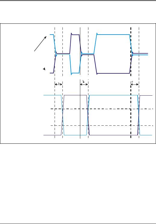
Figure 5-14 on page 108 illustrates the FS driver and receiver waveforms. Note that the driver impedance (28Ω -44Ω ) and cable impedance (90Ω ) are not matched, so reflections from the receiver end of the cable are expected. The initial driver transition is sufficient to cause a wave front and subsequent reflection at the target device. The reflection at the receiver end causes the receiver to detect the signal transition. The driver is roughly halfway through its full voltage swing when the target detects the transition, resulting in a one-way cable delay of 26ns.
107
USB System Architecture
Figure 5-14: Full-Speed Driver and Receiver Waveforms
2XWSXW 'ULYHU 6LJQDO 3LQV 
 &DEOH 'HOD\
5HFHLYHU 6LJQDO 3LQV
9,+ PD[
9,/ PLQ
Low-Speed Drivers
Low-speed buffers drive their signal across an untwisted wire cable and must only be used when transmitting information between low-speed hub ports and low-speed devices. The rise and fall time of the low-speed signals on this cable must be greater than 75ns to keep RFI within FCC class B limits, and must be less than 300ns to limit timing delays and signaling skew. Using the slew rate specified, the driver must reach the specified static signal levels with smooth rise and fall times and must exhibit minimal reflections and ringing.
Signaling conventions used by low-speed drivers are based on the D- line being terminated at the device with a 1.5KΩ resistor. The resulting idle state for a lowspeed device is a differential “0.”
108