


CHAPTER 2. THE ARCHITECTURE OF MODERN GRAPHICS PROCESSORS
some sense, texture memory can be used, with restrictions, as a way of caching global memory in a transparent way for the programmer.
On-chip memory spaces
Due to the high penalty introduced by the access to DRAM, on-chip SRAM memories play a key role in the final performance attained by general-purpose applications. We describe on-chip memory spaces dividing them into shared memory and caches.
Shared memory
Shared memory resides on chip (SRAM) and is only visible to the threads in the same CTA. It is dynamically allocated and only occupies space since the creation of the CTA until its destruction. As it resides on chip, shared memory tra c does not interfere with global memory tra c, and does not share its bandwidth limitations. In practice, it is useful to build very high-bandwidth memory structures on chip that support the high-demanding read/write needs of each SM. In fact, shared memories are usually exploited as small caches (usually known as scratchpad memories) whose integrity and coherence is managed by software. As threads in each CTA can potentially generate di erent shared memory addresses at each instruction, shared memory is usually divided in banks that are independently addressable. In the NVIDIA 8800, shared memory is divided into 16 independent blocks; in general, this quantity is large enough to deliver a high throughput unless pathological cases of unique addressing are given. Avoiding bank conflicts is another important aspect to attain high performance in GPU computing.
Caches
Graphics routines often involve working with large data sets, usually in the order of Mbytes, to generate one single frame. The graphics-oriented nature of the GPU makes it unpractical to build caches on chip which are large enough to hold a significant fraction of the necessary data for the computation close to the processing unit. Modern GPUs o er texture caches that store read-only data fetched from DRAM. From the GPGPU perspective, these caches can be exploited to avoid unnecessary global memory access for certain data structures. As for graphics workloads, these caches are for read-only memory chunks. The latest models of GPUs from NVIDIA (Fermi) include for the first time L1 caches mapped in the same SRAM space devoted to shared memory. However, the management of these memory spaces is performed by hardware, without the programmer’s intervention, which simplifies the development process and has a direct impact on performance.
2.4.The GPU as a part of a hybrid system
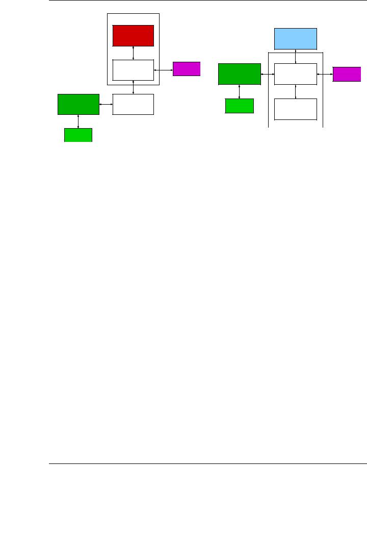
GPUs do not work as an isolated device, but as a component of a hybrid architecture in conjunction with the CPU, chipset, system memory and, possibly, other graphics processors. Figure 2.6 illustrates two common configurations of current hybrid CPU-GPU systems. Although future trends advocate for the integration of CPU and GPU in the same die, current architectures are based on discrete GPUs, usually attached to the rest of the system through a high speed bus. The schema in the left of the figure shows a typical configuration for an AMD-based architecture. In this case, the North Bridge is integrated into the die, and the GPU connects directly to the chipset through the PCIExpress Gen2 bus. The organization in the right of the figure shows the distribution of elements in an Intel-based architecture. Observe how the GPU is attached directly to the North
28
2.4. THE GPU AS A PART OF A HYBRID SYSTEM |
|
|
|
|
|||
|
|
AMD CPU |
|
|
|
|
|
|
|
CPU core |
|
|
Intel CPU |
|
|
|
|
|
|
|
|
||
|
|
Internal Bus |
|
|
|
Chipset |
|
|
|
|
|
|
FSB |
|
|
|
|
North Bridge |
RAM |
|
|
|
RAM |
|
|
Memory |
|
North Bridge |
|||
|
|
128 b. |
GPU |
||||
|
|
667 Mb/s |
|
Memory |
|||
|
|
|
|
PCIe |
128 b. |
||
|
|
|
|
|
8 Gb/s |
667 Mb/s |
|
|
|
|
|
|
|
|
|
|
|
HyperTransport |
|
100 Gb/s |
|
|
|
|
|
|
|
|
|
|
|
GPU |
PCIe |
Chipset |
|
GPU |
|
|
|
|
Memory |
South Bridge |
|
||||
|
|
|
|
||||
|
8 Gb/s |
|
|
|
|||
|
|
|
|
|
|
|
|
100 Gb/s |
|
|
|
|
|
|
|
GPU |
|
|
|
|
|
|
|
Memory |
|
|
|
|
|
|
|
|
(a) AMD configuration |
|
|
(b) Intel configuration |
|
||
Figure 2.6: Examples of two contemporary architectures for hybrid CPU-GPU systems. (a) with an AMD CPU; (b) with an Intel CPU.
Bridge via a 16-lane PCIExpress Gen2 link. This interface provides a peak of 16 Gbytes/s transfer (a peak of 8 Gbytes/s in each direction). In multi-GPU systems, the PCIExpress bus is shared by all the graphics processors.
Hybrid systems present more than one memory address space. More specifically, there is an independent memory address space per GPU, plus the one bound to the CPU system memory. This implies a constant movement of data through the PCIExpress bus. These transfers are critical as the number of GPUs is increased, since data transfers grow then, and e ective bandwidth is reduced.
Figure 2.6 provides information about the bandwidth in the interconnections between the elements in the architectures. Note how the closer buses are to the CPU, the faster they are. As a remarkable exception, GPU memory is fastest than system memory, due to the graphics design requirements. The bandwidth rates shown in the figure can vary for specific system configurations, but are an illustrative example of the transfer rates available in current GPU-based desktop and HPC architectures.
The PCIExpress bus
PCIExpress (formerly known as 3GIO, Third Generation I/O Interface) was introduced in response to the necessity of increasing bandwidths in system buses and memory interfaces during the early 2000s, to keep pace with the processor. By that time, the PCI bus had become a real bottleneck for the growing bandwidth demands from the processors and I/O devices. The parallel approach of the older PCI bus dramatically limited the future of this type of interconnection. The PCI bus was close to its practical limits of performance: it could not be scaled up in frequency or down in voltage, as its synchronous data transfer was dramatically limited by signal skew. This constraint finally derived in a wide variety of interconnection links adapted to the application necessities (AGP for graphics, USB for external devices interconnection, ATA for disk interfaces, PCI for other devices,. . . ). In addition, a common architecture must deal with concurrent data transfers at increasing rates. It was no acceptable that all data transfers are treated in the same way.
29
CHAPTER 2. THE ARCHITECTURE OF MODERN GRAPHICS PROCESSORS
PCIExpress |
|
Base |
Interconnect |
Bandwidth |
Total Bandwidth |
specification |
|
frequency |
Bandwidth |
Lane/direction |
for x16 link |
|
|
(Ghz) |
(Gbits/s) |
(Mbytes/s) |
(Gbytes/s) |
|
|
|
|
|
|
PCIe 1.x |
|
2.5 |
2 |
250 |
8 |
PCIe 2.x |
|
5.0 |
4 |
500 |
16 |
PCIe 3.0 |
|
8.0 |
8 |
1000 |
32 |
Table 2.1: Summary of the bit rate and approximate bandwidths for the various generations of the PCIe architecture
A new standard that o ered both higher bandwidth and enough flexibility to deal with di erent bandwidth demands was necessary.
The design of the PCIExpress specification presented some basic requirements:
Flexibility to adapt to a wide variety of bandwidth-demanding devices, from network interfaces (Gigabit Ethernet and InfiniBand) to graphics devices. PCIExpress was the natural substitute of the AGP port for the connection of graphics devices.
Performance and scalability by adding additional lanes to the bus, higher bandwidth per pin, low overhead in communications and low latency.
Support for a variety of connection types: chip-to-chip, board-to-board via connector, docking station, and mobile devices. This ability makes it possible to physically separate devices from hosts, as in the TESLA s1070 multi-GPU system used in this work.
Compatibility with former PCI software model.
Advanced features as hot-plugging, power management, error handling, QoS, etc.
A basic PCIExpress link consists of two pairs of signals: a transmit pair and a receive pair. An 8b/10b data encoding scheme is used to attain high data rates. The initial frequency is 2.5 GHz, attaining a peak bandwidth of 250 Mbytes/s per direction. The initial plans were to increase this rate to 10 GHz, which is the upper limit for transmitting signals on copper). Note the serial approach in contrast to the parallel design of the original PCI bus. The bandwidth of a link can be linearly scaled with the addition of new signal pairs to form new lanes. The physical layer of the initial specification supported 1x, 2x, 4x, 8x, 16x and 32x lane widths. Compatibility between devices is negotiated during initialization. The PCIExpress architecture can be eventually improved by upgrading speed and implementing more advanced encoding techniques. This is the case of PCIExpress 2.0 or Gen2, that doubles the base frequency to 5 GHz to attain the same transfer rate using half of the lanes of its predecessor, as the base bandwidth is doubled to 500 Mbytes/s per direction. Future PCIExpress 3.0 will deliver about 1 GByte/s of bandwidth per lane direction, by increasing the base frequency and eliminating the overhead of the 8b/10b encoding scheme, using a more e cient 128b/130b coding scheme. Table 2.1 summarizes the evolution in performance of the PCIExpress specifications, including the eventual PCIExpress 3.0.
2.5.Arithmetic precision. Accuracy and performance
Accuracy was one of the historical problems in GPU computing. Together with the evolution of the graphics architectures, the fixed-point arithmetic of GPUs has evolved from 16-bit, 24-bit,
30

2.6. PRESENT AND FUTURE OF GPU ARCHITECTURES
32-bit to the current single precision (32-bit) IEEE 754-compliant floating-point arithmetic. In addition, recent GPUs also provide for double-precision (64-bit) IEEE 754-compliant floating-point operations. Even though double precision is not necessary in the type of computations the GPUs are designed for, this capability has been added in order to satisfy the demands of many scientific applications.
Single precision floating-point operations supported by the GPU cores include addition, multiplication, multiply-add, minimum, maximum, compare, set predicate, and conversions between integer and floating-point numbers [80]. Most modern GPUs implement floating-point addition and multiplication that are fully compatible with the IEEE 754 standard for single precision floatingpoint numbers, including NaN and infinity values. The most common operation o ered by GPUs is often the multiply-add instruction (madd). In practice, this operation performs a floating-point multiplication with truncation [80], followed by a floating-point addition with round-to-nearest- even. This operation is thus composed of two floating-point operations, and can be performed in only one cycle. No intervention of the instruction scheduler is needed to dispatch two di erent operations. However, the computation is not fused and the product is truncated before the addition is performed.
Special functions such as cosine, sine, binary exponential, binary logarithm, reciprocal and reciprocal square root are available and executed in the SFUs. Although the IEEE 754 standard requires exact-rounding for these operations, many GPU application do not require such an exact compliance. In this domain, higher throughput is preferred to exact accuracy. However, software libraries (CUDA) provide both a full accuracy function and a fast function with the native SFU accuracy.
The floating-point addition and multiplication units are fully pipelined. Although they are also fully pipelined, special operations (executed in the SFUs) yield a throughput smaller than that of floating-point addition and multiplication. A ratio 1/4 is common when comparing both types of operations. This factor, however, is higher than that o ered by the CPUs for common special operations like division or square root, even though CPUs deliver higher accuracy.
Double-precision capabilities have been added to the latest generations of GPUs. These processors support 64-bit IEEE 754 operations in hardware. These operations include addition, multiplication and conversion between di erent floating-point and integer formats. These three operations are performed in hardware in a FMA (fused multiply-add) unit. Unlike for single-precision floatingpoint, the FMA unit in modern GPUs performs a fused-multiply-add operation without truncation of the result after the multiplication. Thus, accuracy is kept in intermediate operations. This unit also enables the formulation of accurate divisions and square roots in software, without needing a special function unit for double-precision arithmetic.
2.6.Present and future of GPU architectures
In the last four years, the number of transistors in the successive generations of NVIDIA hardware has multiplied by four, close to the improvement rate dictated by Moore’s law. In addition, the number of cores (SPs) per GPU has roughly doubled every two years. However, none of the newest hardware developments has been revolutionary; instead, they can be viewed just as the natural evolution of the original G80 implementation with unified architecture. In this section, we will review the main changes introduced by the GT200 and the recently introduced Fermi microarchitectures, remarking the main di erences with the original unified implementation.
Table 2.2 summarizes the main di erences between those three instances of the unified architecture. Only those features with a relevant impact on general-purpose computing have been listed
31