


2.3. THE ARCHITECTURE OF MODERN GRAPHICS PROCESSORS
The implication for the GPGPU field rapidly became notorious. The unified architecture implies more arithmetic units at the disposal of the programmer, each of them with an improved functionality.
Together with the evolution of the processors towards a unified architecture, the software also experienced a drastic revolution with the introduction of the CUDA architecture and the CUDA programming paradigm, both by NVIDIA [1]. The aim of CUDA is to define an implementation of the unified architecture focused on performance and programmability.
The first GPU that implemented the unified architecture following the CUDA guidelines was the NVIDIA G80. Despite being a design from 2006, it is still the base of the newest generations of GPUs from NVIDIA, and no major changes have been introduced in the architecture. Actually, the NVIDIA G80 implemented the directives of Microsoft DirectX 10 [97], which dictated the fusion of the functionality of vertex and pixel shaders, and the addition of geometry shaders, with no real use for GPGPU. Although it was the first GPU complying those requirements, since then other companies have adopted this unified architecture.
2.3.The architecture of modern graphics processors
GPUs with unified architecture are built as a parallel array of programmable processors. Vertex, geometry and pixel shaders are merged, o ering general-purpose computation on the same type of processors, unlike previous generations of GPUs. This programmable array collaborate with other fixed-function processing units that are devoted exclusively to graphics computing. Compared with multi-core CPUs, GPUs have a completely di erent perspective from the design point of view. These di erences are mostly translated into a larger number of transistors devoted to computation, and less to on-chip caches and other functionality.
2.3.1.General architecture overview. Nvidia Tesla
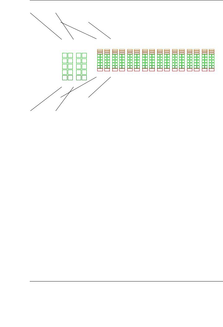
A unified GPU processor array contains a number of processor cores, usually organized into groups or clusters acting as multi-threaded multiprocessors. Figure 2.5 shows the usual architecture of a unified GPU. Each processing unit is known as a Streaming Processor (SP). SPs are organized as a set of clusters usually referred to as Streaming Multiprocessors (SM). Each SP is highly multi-threaded, and handles thread deployment, execution and destruction exclusively in hardware. This provides an execution environment which can deal with thousands of threads without major overheads. The array is connected via a high-speed network to a partitioned memory space.
The basic Tesla architecture appeared in 2006, codenamed TESLA. The first GPU that implemented this architecture was the NVIDIA 8800. In this architecture, the processor array was composed of 128 SPs, grouped in clusters (SMs) of 8 SPs each, and connected with four 64-bit-wide DRAM partitions. In addition, each SM had two special function units (SFUs), instruction and data caches, a multi-threaded instruction unit, and a small shared memory of 16 Kbytes shared by all the SPs of the cluster. Two SMs share a texture unit in each texture/processor cluster (TPC). Originally, an array of eight TPCs composed the so-called Streaming Processor Array, or SPA, which in fact is the unified core which executes all graphics shader programs as well as, in our case, general-purpose programs.
This type of architectures are scalable in two di erent directions. First, the number of SMs in the chip can be increased further. Second, the number of SPs in each cluster can be enlarged, keeping constant the number of SMs. Section 2.6 discusses these possibilities and the solutions adopted by the latest generations of GPUs in order to deliver higher levels of performance.
23
CHAPTER 2. THE ARCHITECTURE OF MODERN GRAPHICS PROCESSORS
|
|
|
|
|
|
|
|
|
|
|
|
|
|
|
|
|
|
|
|
|
|
|
|
|
|
CPU |
|
|
|
|
|
|
|
|
|
|
|
|
BRIDGE |
|
|
|
|
|
|
|
|
SYSTEM MEMORY |
|
|
|
|||||||||||||||||||||||||||||||||||||||||||||
|
|
|
|
|
|
|
|
|
|
|
|
|
|
|
|
|
|
|
|
|
|
|
|
|
|
|
|
|
|
|
|
|
|
|
|
|
|
|
|
|
|
|
|
|
|
|
|
|
||||||||||||||||||||||||||||||||||||||||||||||||
|
SM |
|
|
|
|
|
|
|
|
|
|
|
|
|
|
|
|
|
|
|
|
|
|
|
|
|
|
|
|
|
|
|
|
|
|
|
|
|
|
|
|
|
|
|
|
|
|
|
|
|
|
|
|
|
|
|
|
|
|
|
|
|
|
|
|
|
|
|
|
|
|
|
|
|
|
|
|
|
|
|
|
|
|
|
|
|
|
|
|
|
|
|
|
|||
|
|
|
|
|
|
|
|
|
|
|
|
|
GPU |
|
|
|
|
|
|
|
|
|
|
|
|
|
|
|
|
|
|
|
|
|
|
|
|
|
|
|
|
|
|
|
|
|
|
|
|
|
|
|
|
|
|
|
|
|
|
|
|
|
|
|
|
|
|
|
|
|
|
|
|
|
|
|
|
|
|
|
|
|
|
|
|
|||||||||||
|
|
|
|
|
|
|
|
|
|
|
|
|
|
|
|
|
|
|
|
|
|
|
|
|
|
|
|
|
|
|
|
|
|
|
|
|
|
|
|
|
|
|
|
|
|
|
|
|
|
|
|
|
|
|
|
|
|
|
|
|
|
|
|
|
|
|
|
|
|
|
|
|
|
|
|
|
|
|||||||||||||||||||
|
I-Cache |
|
|
|
|
|
|
|
|
|
|
|
|
|
|
|
|
|
|
|
|
|
|
|
|
|
|
|
|
|
|
|
|
|
|
HOST INTERFACE |
|
|
|
|
|
|
|
|
|
|
|
|
|
|
|
|
|
|
|
|
|
|
|
|
|
|
|
|||||||||||||||||||||||||||||||||
|
|
|
|
|
|
|
|
TPC |
|
|
|
|
|
|
|
|
|
|
|
|
|
|
|
|
|
|
|
|
|
|
|
|
|
|
|
|
|
|
|
|
|
|
|
|
|
|
|
|
|
|
|
|
|
|
|
|
|
|
|
|
|
|
|
|
|
|
|
|
|
|
|
|
|
|
|
|
|
|
|
|
|
|
|
|
|
|
|
|
|
|||||||
|
MT Issue |
|
|
|
|
|
|
|
|
|
|
|
|
|
|
|
|
|
|
|
|
|
|
|
|
|
|
|
|
|
|
|
|
|
|
|
|
|
|
|
|
|
|
|
|
|
|
|
|
|
|
|
|
|
|
|
|
|
|
|
|
|
|
|
|
|
|
|
|
|
|
|
|
|
|
|
|
|
|
|
|
|
|
|
|
|
|
|
|
|
|
|
|
|
||
|
|
|
Geom. Control. |
|
|
|
|
|
|
|
|
|
|
|
|
|
|
|
|
|
|
|
|
|
COMPUTE WORK DISTRIBUTION |
|
|
|
|
|
|
|
|
|
|
|
|
|
|
|
|
|
|
|
|
|
|
|
|
|||||||||||||||||||||||||||||||||||||||||||||||
|
|
|
|
|
|
|
|
|
|
|
|
|
|
|
|
|
|
|
|
|
|
|
|
|
|
|
|
|
|
|
|
|
|
|
|
|
|
|
|
|
|
|
|
|
|
|
|
|
|
|
||||||||||||||||||||||||||||||||||||||||||||||
|
|
|
|
|
|
|
|
|
|
|
|
|
|
|
|
|
|
|
|
|
|
|
|
|
|
|
|
|
|
|
|
|
|
|
|
|
|
|
|
|
|
|
|
|
|
|
|
|
|
|
|
|
|
|
|
|
|
|
|
|
|
|
|
|
|
|
|
|
|
|
|
|
|
|
|
|
|
|
|
|
|
|
|
|
|
|
|
|
|
|
|
|
|
|
|
|
|
C-Cache |
|
|
|
|
SMC |
|
|
|
|
|
|
|
|
|
|
|
|
|
|
|
|
|
|
|
|
|
|
|
|
|
|
|
|
|
|
|
|
|
|
|
|
|
|
|
|
|
|
|
|
|
|
|
|
|
|
|
|
|
|
|
|
|
|
|
|
|
|
|
|
|
|
|
|
|
|
|
|
|
|
|
|
|
|
|
|
|
|||||||||
|
|
|
|
|
|
|
|
|
|
|
|
|
|
|
|
|
|
|
|
|
|
|
|
|
|
|
|
|
|
|
|
|
|
|
|
|
|
|
|
|
|
|
|
|
|
|
|
|
|
|
|
|
|
|
|
|
|
|
|
|
|
|
|
|
|
|
|
|
|
|
|
|
|
|
|
|
|
|
|
|
|
|
|
|
|
|
|
|
|
|
|
|
|
|
|
|
|
SP |
|
SP |
|
|
SM |
|
|
SM |
|
|
|
|
|
|
|
|
|
|
|
|
|
|
|
|
|
|
|
|
|
|
|
|
|
|
|
|
|
|
|
|
|
|
|
|
|
|
|
|
|
|
|
|
|
|
|
|
|
|
|
|
|
|
|
|
|
|
|
|
|
|
|
|
|
|
|
|
|
|
|
|
|
|
|
|
|
|
|
|
|
||||||
|
|
|
|
|
|
|
|
|
|
|
|
|
|
|
|
|
|
|
|
|
|
|
|
|
|
|
|
|
|
|
|
|
|
|
|
|
|
|
|
|
|
|
|
|
|
|
|
|
|
|
|
|
|
|
|
|
|
|
|
|
|
|
|
|
|
|
|
|
|
|
|
|
|
|
|
|
|
|
|
|
|
|
|
|
|
|
|
|
|
|
|
|
|
|
||
|
|
|
|
|
|
|
|
|
|
|
|
|
|
|
|
|
|
|
|
|
|
|
|
|
|
|
|
|
|
|
|
|
|
|
|
|
|
|
|
|
|
|
|
|
|
|
|
|
|
|
|
|
|
|
|
|
|
|
|
|
|
|
|
|
|
|
|
|
|
|
|
|
|
|
|
|
|
|
|
|
|
|
|
|
|
|
|
|
|
|
|
|||||
|
|
|
|
|
|
|
|
|
|
|
|
|
|
|
|
|
|
|
|
|
|
|
|
|
|
|
|
|
|
|
|
|
|
|
|
|
|
|
|
|
|
|
|
|
|
|
|
|
|
|
|
|
|
|
|
|
|
|
|
|
|
|
|
|
|
|
|
|
|
|
|
|
|
|
|
|
|
|
|
|
|
|
|
|
|
|
|
|
|
|
|
|
|
|
|
|
|
|
|
|
|
|
|
|
|
|
|
|
|
|
|
|
|
|
|
|
|
|
|
|
|
|
|
|
|
|
|
|
|
|
|
|
|
|
|
|
|
|
|
|
|
|
|
|
|
|
|
|
|
|
|
|
|
|
|
|
|
|
|
|
|
|
|
|
|
|
|
|
|
|
|
|
|
|
|
|
|
|
|
|
|
|
|
|
|
|
|
|
|
|
|
|
|
|
|
|
|
|
|
|
|
|
|
|
|
|
|
|
|
|
|
|
|
|
|
|
|
|
|
|
|
|
|
|
|
|
|
|
|
|
|
|
|
|
|
|
|
|
|
|
|
|
|
|
|
|
|
|
|
|
|
|
|
|
|
|
|
|
|
|
|
|
|
|
|
|
|
|
|
|
|
|
|
|
|
|
|
|
|
|
|
|
|
|
|
|
|
|
|
|
|
SP |
|
SP |
|
|
SP |
|
SP |
|
|
|
SP |
|
SP |
|
|
|
|
|
|
|
|
|
|
|
|
|
|
|
|
|
|
|
|
|
|
|
|
|
|
|
|
|
|
|
|
|
|
|
|
|
|
|
|
|
|
|
|
|
|
|
|
|
|
|
|
|
|
|
|
|
|
|
|
|
|
|
|
|
|
|
|
|
|
|
|
|
|
|
|
|
|
|
|
|
|
|
|
|
|
|
|
|
|
|
|
|
|
|
|
|
|
|
|
|
|
|
|
|
|
|
|
|
|
|
|
|
|
|
|
|
|
|
|
|
|
|
|
|
|
|
|
|
|
|
|
|
|
|
|
|
|
|
|
|
|
|
|
|
|
|
|
|
|
|
|
|
|
|
|
|
|
|
|
|
|
|
|
|
|
|
|
|
|
|
|
|
||||||
|
|
|
|
|
|
|
|
|
|
|
|
|
|
|
|
|
|
|
|
|
|
|
|
|
|
|
|
|
|
|
|
|
|
|
|
|
|
|
|
|
|
|
|
|
|
|
|
|
|
|
|
|
|
|
|
|
|
|
|
|
|
|
|
|
|
|
|
|
|
|
|
|
|
|
|
|
|
|
|
|
|
|
|
|
||||||||||||
|
|
|
|
|
|
|
|
|
|
|
|
|
|
|
|
|
|
|
|
|
|
|
|
|
|
|
|
|
|
|
|
|
|
|
|
|
|
|
|
|
|
|
|
|
|
|
|
|
|
|
|
|
|
|
|
|
|
|
|
|
|
|
|
|
|
|
|
|
|
|
|
|
|
|
|
|
|
|
|
|
|
|
|
|
|
|
|
|
|
|
|
|
|
|
||
|
|
|
|
|
|
SP |
|
SP |
|
|
|
SP |
|
SP |
|
|
|
|
|
|
|
|
|
|
|
|
|
|
|
|
|
|
|
|
|
|
|
|
|
|
|
|
|
|
|
|
|
|
|
|
|
|
|
|
|
|
|
|
|
|
|
|
|
|
|
|
|
|
|
|
|
|
|
|
|
|
|
|
|
|
|
|
|
|
|
|
|
|
|
|
|
|
|
|
|
|
|
|
|
|
|
|
|
|
|
|
|
|
|
|
|
|
|
|
|
|
|
|
|
|
|
|
|
|
|
|
|
|
|
|
|
|
|
|
|
|
|
|
|
|
|
|
|
|
|
|
|
|
|
|
|
|
|
|
|
|
|
|
|
|
|
|
|
|
|
|
|
|
|
|
|
|
|
|
|
|
|
|
|
|
|
|
|
|
|
|
|
|
|
||||
|
|
|
|
|
|
|
|
|
|
|
|
|
|
|
|
|
|
|
|
|
|
|
|
|
|
|
|
|
|
|
|
|
|
|
|
|
|
|
|
|
|
|
|
|
|
|
|
|
|
|
|
|
|
|
|
|
|
|
|
|
|
|
|
|
|
|
|
|
|
|
|
|
|
|
|
|
|
|
|
|
|
|
|
|
|
|
|
|
|
|
|
|
|
|
|
|
|
SP |
|
SP |
|
|
SP |
|
SP |
|
|
|
SP |
|
SP |
|
|
|
|
|
|
|
|
|
|
|
|
|
|
|
|
|
|
|
|
|
|
|
|
|
|
|
|
|
|
|
|
|
|
|
|
|
|
|
|
|
|
|
|
|
|
|
|
|
|
|
|
|
|
|
|
|
|
|
|
|
|
|
|
|
|
|
|
|
|
|
|
|
|
|
|
|
|
|
|
|
|
|
|
|
|
|
|
|
|
|
|
|
|
|
|
|
|
|
|
|
|
|
|
|
|
|
|
|
|
|
|
|
|
|
|
|
|
|
|
|
|
|
|
|
|
|
|
|
|
|
|
|
|
|
|
|
|
|
|
|
|
|
|
|
|
|
|
|
|
|
|
|
|
|
|
|
|
|
|
|
|
|
|
|
|
|
|
|
|
|
|
|
|
|
|
|
||
|
|
|
|
|
|
SP |
|
SP |
|
|
|
SP |
|
SP |
|
|
|
|
|
|
|
|
|
|
|
|
|
|
|
|
|
|
|
|
|
|
|
|
|
|
|
|
|
|
|
|
|
|
|
|
|
|
|
|
|
|
|
|
|
|
|
|
|
|
|
|
|
|
|
|
|
|
|
|
|
|
|
|
|
|
|
|
|
|
|
|
|
|
|
|
|
|
|
|
|
|
|
|
|
|
|
|
|
|
|
|
|
|
|
|
|
|
|
|
|
|
|
|
|
|
|
|
|
|
|
|
|
|
|
|
|
|
|
|
|
|
|
|
|
|
|
|
|
|
|
|
|
|
|
|
|
|
|
|
|
|
|
|
|
|
|
|
|
|
|
|
|
|
|
|
|
|
|
|
|
|
|
|
|
|
|
|
|
||||||||||
|
|
|
|
|
|
|
|
|
|
|
|
|
|
|
|
|
|
|
|
|
|
|
|
|
|
|
|
|
|
|
|
|
|
|
|
|
|
|
|
|
|
|
|
|
|
|
|
|
|
|
|
|
|
|
|
|
|
|
|
|
|
|
|
|
|
|
|
|
|
|
|
|
|
|
|
|
|
|
|
|
|
|
|
|
|
|
|
|
|
|
|
|
|
|
|
|
|
SP |
|
SP |
|
|
|
|
|
|
|
|
|
|
|
|
|
|
|
|
|
|
|
|
|
|
|
|
|
|
|
|
|
|
|
|
|
|
|
|
|
|
|
|
|
|
|
|
|
|
|
|
|
|
|
|
|
|
|
|
|
|
|
|
|
|
|
|
|
|
|
|
|
|
|
|
|
|
|
|
|
|
|
|
|
|
|
|
|
|
|
|
|
|
|
|
|
|
|
|
|
|
|
|
|
|
|
|
|
|
|
|
|
|
|
|
|
|
|
|
|
|
|
|
|
|
|
|
|
|
|
|
|
|
|
|
INTERCONNECTION NETWORK |
|
|
|
|
|
|
|
|
|
|
|
|
|
|
|
|
|
|
|
|
|
|
|
|
|||||||||||||||||||||||||||||||||
|
|
|
|
|
|
|
|
|
|
|
|
|
|
|
|
|
|
|
|
|
|
|
|
|
|
|
|
|
|
|
|
|
|
|
|
|
|
|
|
|
|
|
|
|
|
|
|
|
|
|
|
|
|
|
|
|
|
|
|
|
|
|
|
|
||||||||||||||||||||||||||||||||
|
SFU |
|
SFU |
|
|
Texture Unit |
|
|
|
|
|
|
|
|
|
|
|
|
|
|
|
|
|
|
|
|
|
|
|
|
|
|
|
|
|
|
|
|
|
|
|
|
|
|
|
|
|
|
|
|
|
|
|
|
|
|
|
|
|
|
|
|
|
|
|
|
|
|
|
|
|
|
|
|
|
|
|
|
|
|
|
|
|
|
|
|
|
|
||||||||
|
|
|
|
Tex L1 Cache |
|
|
|
ROP |
|
|
|
L2 |
|
|
|
|
|
|
|
ROP |
L2 |
|
|
|
|
ROP |
|
|
|
L2 |
|
|
|
|
|
|
|
|
|
ROP |
|
L2 |
|
|||||||||||||||||||||||||||||||||||||||||||||||||||||
|
|
|
|
|
|
|
|
|
|
|
|
|
|
|
|
|
|
|
|
|
|
|
|
|
|
|
|
|
|
|
|
|
|
|
|
|
||||||||||||||||||||||||||||||||||||||||||||||||||||||||||||
|
|
|
|
|
|
|
|
|
|
|
|
|
|
|
|
|
|
|
|
|
|
|
|
|
|
|
|
|
|
|
|
|
|
|
|
|
|
|
|
|
|
|
|
|
|
|
|
|
|
|
|
|
|
|
|
|
|
|
|
|
|
|
|
|
|
|
|
|
|
|
|
|
|
|
|
|
|
|
|
|
|
|
|
|
|
|
|
|
|
|
|
|
|
|
|
|
|
|
|
|
|
|
|
|
|
|
|
|
|
|
|
|
|
|
|
|
|
|
|
|
|
|
|
|
|
|
|
|
|
|
|
|
|
|
|
|
|
|
|
|
|
|
|
|
|
|
|
|
|
|
|
|
|
|
|
|
|
|
|
|
|
|
|
|
|
|
|
|
|
|
|
|
|
|
|
|
|
|
|
|
|
|
|
|
|
|
|
|
|
|
|||
|
Shared |
|
|
|
|
|
|
|
|
|
|
|
|
|
|
|
|
|
|
|
|
|
|
|
|
|
|
|
|
|
|
|
|
|
|
|
|
|
|
|
|
|
|
|
|
|
|
|
|
|
|
|
|
|
|
|
|
|
|
|
|
|
|
|
|
|
|
|
|
|
|
|
|
|
|
|
|
|
|
|
|
|
|
|
|
|
|
|
|
|
|
|
|
|
||
|
Memory |
|
|
|
|
|
|
|
|
|
|
|
|
|
|
|
|
|
|
|
DRAM |
|
|
|
|
|
|
|
|
|
|
DRAM |
|
|
|
|
|
|
DRAM |
|
|
|
|
|
|
|
|
|
|
|
|
DRAM |
|
|||||||||||||||||||||||||||||||||||||||||||
|
|
|
|
|
|
|
|
|
|
|
|
|
|
|
|
|
|
|
|
|
|
|
|
|
|
|
|
|
|
|
|
|
|
|
|
|
|
|
|
|
|
|
|
|
|
|
|
|
|
|
|
|
|
|
|
|
|
|
|
|
|
|
|
|
|
|
|
|
|
|
|
|
|
|
|
|
|
|
|
|
|
|
|
|
|
|
|
|
|
|
|
|
|
|
|
|
Figure 2.5: Unified architecture implementation on the NVIDIA TESLA series.
Single-Instruction Multiple-Threads (SIMT paradigm)
To e ciently manage the vast number of threads that execute a kernel, the multiprocessor exhibits a single-instruction multiple-thread (SIMT) architecture. The SIMT architecture concurrently applies one instruction to multiple independent threads during the parallel execution of a kernel. The multiprocessor is in charge of the creation, management, scheduling and execution of threads grouped in the so-called warps. A warp is a set of parallel threads executing the same instruction together in an SIMT architecture. In practice, the warp is the minimum scheduling unit of threads to SMs. At each scheduling step, a group of threads are bundled and issued to an SM, in which they logically execute in parallel. A correct management of divergence and memory access patterns within the threads in a warp is a key factor in the final performance of current GPU implementations.
The Streaming Processor Array (SPA)
We next describe in detail the architecture of the NVIDIA 8800 GPU to illustrate a real implementation of the unified architecture. As shown in Figure 2.5, the NVIDIA 8800 implementation has up to 128 SPs organized as 16 SMs. A group of two SPs share a common texture unit; these three elements define a texture cluster. An array of eight texture clusters define the SPA (Streaming Processor Array), the real kernel of a GPU with unified architecture.
The host interface unit communicates the GPU with the CPU via a PCI-Express and performs context switching in hardware. The work distribution units are in charge of dispatching vertices, pixels or, in case of GPGPU computing, compute thread arrays (warps) to the available TPCs in the array. Thus, the TPCs execute vertex and pixel shaders, and also general-purpose computing programs. Graphical output data is sent to specialized hardware units after TPC processing, for
24
2.3. THE ARCHITECTURE OF MODERN GRAPHICS PROCESSORS
example, the ROP units through the interconnection network. This network also routes texture data loaded from the SPA to DRAM and vice-versa via an L2 cache.
Streaming Multiprocessor (SM)
The Streaming Multiprocessor is the basic execution unit of the SPA. The SM is a unified graphics and general-purpose multiprocessor which can execute vertex, geometry, and pixel shaders, together with parallel computing programs. Each SM contains eight SPs, two SFUs, a multithreaded fetch and issue instruction unit, an instruction cache, a constant cache (read-only cache), and 16 Kbytes of on-chip shared memory.
To deal with the execution of hundreds of parallel threads, the SM is hardware multi-threaded. The management and execution of up to 768 concurrent threads is performed in hardware with basically zero-scheduling overhead. This negligible penalty is absolutely necessary to deal with such a large pool of parallel threads and one of the distinctive features of graphics processors with unified architecture.
In the SIMT model previously described, the instruction fetch and issue unit of each SM is shared across 32 threads. The SM schedules and executes warps from a pool of ready warps. An issued warp instruction runs as four sets of 8 thread on four cycles. At each cycle, ready warps are qualified as prepared to be issued using a scoreboard [79]. The instruction scheduler assigns priorities to each warp and selects the first warp in the list for execution during the next issue cycle. This priority is based on the type of the warp (vertex, geometry, pixel or parallel computing), instruction type and other factors to assure a load balance among di erent warp types that execute in the SM.
In practice, the SM execute groups of cooperative thread arrays (also referred as CTAs); logically, CTAs are multiple concurrent warps which can communicate using a fast, on-chip shared memory region.
Instruction set
Unlike previous GPU architectures, in which the instruction set was designed to basically support vector instructions (to process four color channels per pixel), threads execute exclusively scalar instructions. In other words, the unified architecture is basically a scalar architecture. Only texture operations remain to be vector-based. This instruction set is supported by the Streaming Processor implementation, basically a scalar processor without vector capabilities.
The instruction set is register-based, and includes floating-point and integer arithmetic, logical, flow control, texture and load/store instructions. The load/store instructions can access three di erent memory-spaces:
Local memory for per-thread, private and temporary data.
Shared memory for low-latency, per-CTA data that is shared by the threads within a CTA.
Global memory for data shared by all threads that participate in the computations.
In addition, operations for fast barrier synchronization within the threads in a CTA are available.
Streaming Processor (SP)
Each Streaming Processor contains both integer and floating-point arithmetic units to execute most the operations needed by graphics and general-purpose programs. Two key factors characterize the architecture of an SP. First, it is highly hardware multi-threaded, supporting up to 64
25

CHAPTER 2. THE ARCHITECTURE OF MODERN GRAPHICS PROCESSORS
simultaneous threads. Second, each SP presents a large multi-thread register file. Each SP core has a file of 1024 general-purpose 32-bit registers, which are partitioned among the assigned threads mapped for execution in the core.
From the software point of view, this architecture clearly determines the nature of the parallel executions. The vast amount of threads and wide register file requires fine-grained executions with massive multi-threading to exploit the architecture features. CUDA programs often need a small amount of registers (typically between 8 and 32), which ultimately limits the number of threads that will execute a kernel program.
The multiprocessor executes texture fetch instructions and memory load, store and atomic operations concurrently with instructions on the SPs. Shared-memory access (explained later) employs low-latency interconnections between the SPs and shared memory banks inside each SM.
2.3.2.Memory subsystem
The second key factor that ultimately determines the performance of graphics (and generalpurpose) applications is the graphics memory subsystem. From the general-purpose computation perspective, the features of the memory subsystem define the applications that fit better to the GPU, and which algorithms and implementations are well-suited for this class of architecture.
The graphics-oriented nature of the GPUs dictates why the graphics memories have historically been developed at a highest pace compared with central memories. Graphics applications are data-intensive, with high data tra c demands. Consider, for example, the NVIDIA Geforce 8800 described above. From the graphics point of view, it can process up to 32 pixels per cycle, running at 600 MHz [80]. Typically, each pixel requires a color read and a color write, plus a depth read and a depth write for a 4-byte pixel (four color channels). In order to generate a pixel’s color, usually two or even three texels (elements of texture), of four bytes each, are read from texture memory. In a typical case, this demands 28 bytes times 32 pixels = 896 bytes per clock, which is an considerable bandwidth rate that the memory subsystem must provide.
GPU memories usually satisfy a number of features:
Width, o ering a large set of pins to transfer data to and from the chip, and even to perform intra-memory transfers.
Speed, to maximize the data rate by using aggressive signaling techniques.
Usage of explicitly managed memory hierarchies. A large fraction of the transistors in a GPU are devoted to computing power. However, there exist strategic memory spaces (shared memory per SM) or caches (texture cache) that can be exploited by the programmer in order to boost performance.
GPUs are designed to exploit every idle cycle to transfer data to and from global memory. GPUs do not aim to specifically minimize memory latency, but to hide it by increasing the throughput or utilization e ciency (for example, by increasing the number of concurrent threads in the system).
O -chip memory spaces
DRAM chips present some characteristics that must be taken into account in the design of GPUs. DRAM chips are internally built as a set of banks organized by rows (typically around 16,384, and each row with a number of cells (or bits, typically 8,192). Current DRAM limitations require that both GPU architectures and run-time implementations consider these particularities.
26

2.3. THE ARCHITECTURE OF MODERN GRAPHICS PROCESSORS
As an example, the activation of a row in a DRAM bank usually takes dozens of cycles, but once activated, the bits in the row are randomly accessible in a few clock cycles.
In addition, the graphics pipeline presents several sources of data tra c and requests, with high heterogeneity and poor spatial locality. Usually, the GPU memory controller deals with this independent data tra c generators by waiting until enough tra c is generated for a given DRAM row before activating it and transferring the corresponding data. This type of strategies usually have a negative impact on latency, but improve the usage of the bus.
DRAM is usually deployed as multiple memory partitions, each one with an independent memory controller. Usually, addresses are interleaved across all memory partitions in order to optimize the load balance in memory accesses.
The CUDA architecture exposes di erent memory spaces that allow the developer to optimally exploit the computational power of unified GPUs. The following description presents the di erent memory spaces available in the NVIDIA TESLA GPUs, although similar approaches have been taken by other GPU manufacturers.
Global and local memory
Global memory is stored in DRAM partitions. It is meant for the communication among threads that belong to di erent CTAs, so it is not local to any physical SM. Sequential consistency is not guaranteed in the access to global memory by di erent threads. Threads view a relaxed ordering model: within a thread, the order of memory reads and writes to the same address is e ectively preserved; the order of accesses to di erent addresses is not guaranteed to prevail. In order to obtain a strict memory ordering among threads in the same CTA, explicit barrier synchronizations are available. There is also a special thread instruction in the Instruction Set Architecture (membar) that provides a memory barrier to commit previous memory transactions and make them visible to the remaining threads. Atomic global memory operations are also available for threads that cooperate via shared memory addresses.
Local memory is also allocated in external DRAM. It is private memory visible only to a single thread. From the architecture perspective, it is than the large register file available per thread, so it supports large allocations of memory. Note that the total amount of local memory equals the local memory allocated per thread times the total number of active threads.
Local and global memory load/store instructions coalesce individual parallel thread requests from the same warp into a single memory block request if the addresses fall in the same block, and meet some alignment criteria specific to each architecture. Satisfying these restrictions improves memory bandwidth in a remarkable way. This is a very common optimization in CUDA programs, and usually reduces the impact introduced by the usage of external DRAM memories.
Constant and texture memories
Constant memory is also stored in DRAM. It is a read-only memory space, cached in the SM. Its main purpose is to broadcast scalar values to all the threads in a warp, an operation that is very useful for graphics codes.
Texture memory is designed to hold large-arrays of read-only data. Textures can be seen as one-dimensional, two-dimensional or three-dimensional data structures. Texture transfers are performed using special instructions, referencing the name of the texture and the coordinates to be extracted. Texture fetches are also cached in a streaming cache hierarchy, specifically designed to optimize texture fetches from the large amount of active threads present in modern GPUs. In
27