

Digital design with CPLD applications and VHDL (R. Dueck, 2000)
.pdf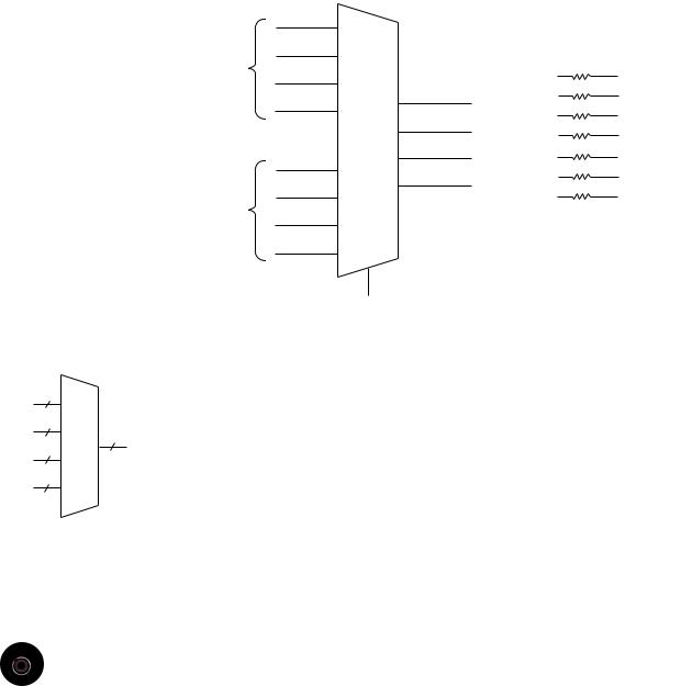
|
|
|
|
|
|
|
|
|
|
|
|
5.3 |
• Multiplexers |
191 |
||||
FIGURE 5.39 |
|
|
|
|
|
|
|
|
|
7-Segment |
|
|
||||||
Quadruple 2-to-1 MUX as a |
|
|
|
0 |
|
BCD/7SEG |
|
Display |
|
|
||||||||
Digital Output Selector |
|
|
|
|
|
|
|
|
|
|
|
|
|
|||||
|
|
|
|
D03 |
|
|
|
|
|
|
|
|
|
|||||
|
|
|
|
|
|
|
|
|
|
|
|
|
|
|
|
|
|
|
|
|
|
|
|
|
|
|
|
1 |
|
|
|
|
|
|
|
|
|
|
|
|
|
|
|
BCD |
|
|
D02 |
|
|
|
|
|
|
|
|
|
|
|
|
|
|
|
0 |
|
0 |
|
|
a |
|
|
|
|
|
|
|
|
|
|
|
|
|
|
|
D01 |
|
|
|
|
|
|
|
|
||
|
|
|
|
|
|
|
|
|
|
|
b |
|
|
|
|
|
|
|
|
|
|
|
|
|
|
|
|
0 |
Y3 |
D3 |
|
|
|
|
|
|
|
|
|
|
|
|
|
|
|
|
D00 |
c |
|
|
|
|
|
|
||
|
|
|
|
|
|
|
|
|
|
|
|
|
|
|
|
|
||
|
|
|
|
|
|
|
|
|
|
Y2 |
D2 |
d |
|
|
|
|
|
|
|
|
|
|
|
|
|
|
|
1 |
Y1 |
D1 |
e |
|
|
|
|
|
|
|
|
|
|
|
|
|
|
|
|
|
|
|
|
|
||||
|
|
|
|
|
|
|
|
|
|
|
|
|
|
|
|
|||
|
|
|
|
|
|
|
|
|
D13 |
|
|
f |
|
|
|
|
|
|
|
|
|
|
|
|
|
|
|
0 |
Y0 |
D0 |
g |
|
|
|
|
|
|
|
|
|
|
|
|
BCD1 |
|
D12 |
|
|
|
|
|
|
|
|
||
|
|
|
|
|
|
|
0 |
|
|
|
|
|
|
|
|
|
||
|
|
|
|
|
|
|
|
|
D11 |
|
|
|
|
|
|
|
|
|
|
|
|
|
|
|
|
|
|
1 |
|
|
|
|
|
|
|
|
|
|
|
|
|
|
|
|
|
|
D10 |
|
|
|
|
|
|
|
|
|
|
|
|
|
|
|
|
|
|
|
|
|
|
|
|
|
|
|
|
|
|
|
|
|
|
|
|
|
S |
|
|
|
|
|
|
|
|
|
|
|
|
|
|
|
|
|
|
|
|
|
|
||||||
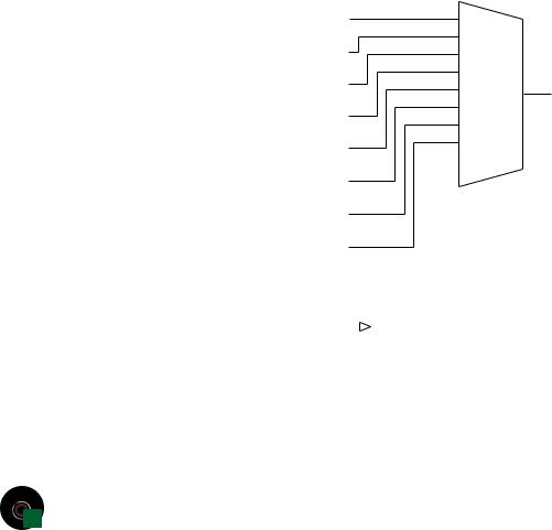
EXAMPLE 5.7 |
|
Draw the symbol for a multiplexer that will select one of four 4-bit channels and direct it to |
||||||||||||||||
|
|
|
|
|
|
a 4-bit output. Create a VHDL file that implements this function and a simulation showing |
||||||||||||
4 |
D0 |
|
the operation of the device. |
|
|
|
|
|
|
|
|
|
||||||
4 |
|
Solution |
Figure 5.40 shows the symbol for the 4-channel, 4-bit multiplexer. This sym- |
|||||||||||||||
|
|
|
||||||||||||||||
4 |
|
bol is shown with the data inputs and outputs in bus form. The data inputs are labelled in |
||||||||||||||||
4 |
D1 |
Y |
||||||||||||||||
D2 |
groups D0 to D3, which contain the individual inputs [D03..D00] to [D33..D30]. |
|
|
|||||||||||||||
|
|
|
|
|
|
|||||||||||||
4 |
|
A VHDL file describing this function is listed below. |
|
|
|
|
|
|
|
|||||||||
D3 |
|
|
|
|
|
|
|
|
||||||||||
|
|
|
|
–— quad4to1.vhd |
|
|
|
|
|
|
|
|
|
|
||||
|
|
|
|
|
|
|
|
|
|
|
|
|
|
|
|
|||
|
|
|
|
|
|
ENTITY quad4to1 IS |
|
|
|
|
|
|
|
|
|
|||
|
|
|
|
|
|
|
|
|
|
|
|
|
|
|
||||
|
|
S1 S0 |
|
PORT( |
|
|
|
|
|
|
|
|
|
|
|
|||
|
|
|
s |
: IN |
INTEGER RANGE 0 to 3; |
|
|
|
|
|
|
|
||||||
|
|
|
|
|
|
|
|
|
|
|
|
|
||||||
FIGURE 5.40 |
|
d0 |
: IN |
BIT_VECTOR (3 downto 0); |
|
|
|
|
|
|
|
|||||||
|
d1 |
: IN |
BIT_VECTOR (3 downto 0); |
|
|
|
|
|
|
|
||||||||
Example 5.7 |
|
|
|
|
|
|
|
|
||||||||||
4-channel 4-bit MUX |
|
d2 |
: IN |
BIT_VECTOR (3 downto 0); |
|
|
|
|
|
|
|
|||||||
|
|
|
|
|
|
d3 |
: IN |
BIT_VECTOR (3 downto 0); |
|
|
|
|
|
|
|
|||
|
|
|
|
|
|
y |
: OUT |
BIT_VECTOR (3 downto 0)); |
|
|
|
|
|
|
|
|||
|
|
|
END quad4to1; |
|
|
|
|
|
|
|
|
|
|
|||||
|
|
quad4to1.vhd |
|
|
|
|
|
|
|
|
|
|
|
|||||
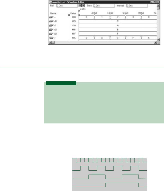
quad4to1.scf
ARCHITECTURE mux4 OF quad4to1 IS BEGIN
–— Selected Signal Assignment MUX4: WITH s SELECT
y <= d0 WHEN 0, d1 WHEN 1, d2 WHEN 2, d3 WHEN 3;
END mux4;
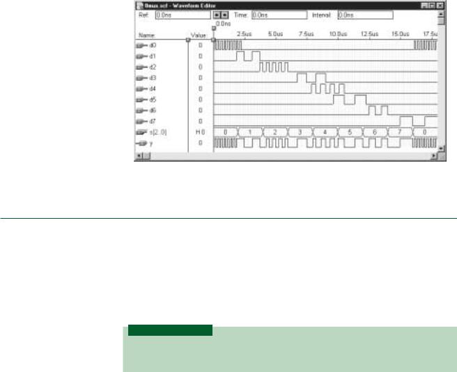
Figure 5.41 shows a set of simulation waveforms for the multiplexer. The D inputs are shown in groups of four, the value of each shown as a steady hexadecimal value. The select inputs are grouped, showing an increasing 2-bit binary count as a hexadecimal value (0 to 3, then repeating). As the S inputs select each group of D inputs, their combined value is directed to the Y output group.
5.3 • Multiplexers |
193 |
waveforms from bottom to top, you will see that they generate a repeating binary sequence (000, 001, 010, 011, 100, 101, 110, 111, 000 . . .).
|
|
MUX |
|
|
D0 |
|
|
|
D1 |
|
|
|
D2 |
|
|
|
D3 |
Y |
|
|
D4 |
||
|
|
||
|
D5 |
|
|
|
D6 |
|
|
|
D7 |
|
|
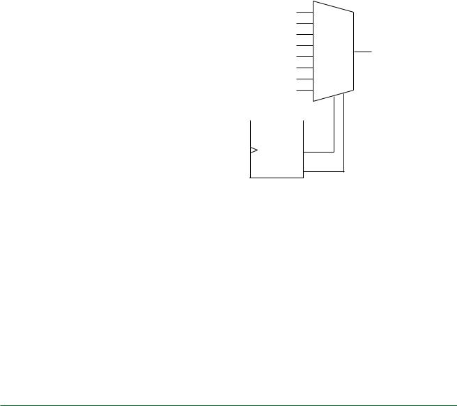
CTR DIV 8 |
|
|
|
|
S2 |
|
|
Q2 |
|
|
|
|
|
|
|
|
|
|
|
S1
CLOCK |
|
Q1 |
|
S0
Q0
FIGURE 5.43
Time-Dependent Selection of Eight Multiplexer Channels
If we connect the counter outputs Q2Q1Q0 to the select inputs of an 8-to-1 MUX, as in Figure 5.43, we will select the channels in sequence, one after the other. The counter is labelled CTR DIV 8 because its most significant bit output has a frequency equal to the clock frequency divided by eight. The triangle on the clock input indicates that it is active when the clock waveform makes a transition from one logic level to another. Since there is no inverting bubble on the clock input, we know that the active clock transition is from LOW to HIGH (i.e., a positive edge).
Waveform Generation. A multiplexer and counter can be used as a programmable waveform generator. The output waveform can be programmed to any pattern by switching the logic levels on the data inputs. This is an easy way to generate an asymmetrical waveform, a task which is more complicated using other digital circuits. The circuit can also generate symmetrical waveforms by alternating the logic levels of consecutive groups of inputs.
EXAMPLE 5.8 |
Draw a circuit that uses an 8-to-1 multiplexer to generate a programmable 8-bit repeating |
||||||||||
|
pattern. Draw the timing diagram of the select inputs and the output waveform for the fol- |
||||||||||
|
lowing pattern of data inputs. |
|
|
|
|
|
|
|
|||
|
|
|
|
|
|
|
|
|
|
|
|
|
|
D7 |
D6 |
|
D5 |
D4 |
D3 |
D2 |
D1 |
D0 |
|
|
|
|
|
|
|
|
|
|
|
|
|
|
|
0 |
1 |
|
1 |
0 |
0 |
1 |
0 |
1 |
|
|
|
|
|
|
|
|
|
|
|
|
|
Solution Figure 5.44a shows the waveform generator circuit. The output waveform with respect to the counter inputs is shown in Figure 5.44b. This pattern is relatively difficult to generate by other means since it has several unequal HIGH and LOW sequences in one period.
194 |
C H A P T E R 5 • Combinational Logic Functions |
|
|
|
|
|
|
FIGURE 5.44 |
|
|
|
|
|
||
Example 5.8 |
|
|
MUX |
|
|||
Programmable Waveform |
|
|
|
||||
|
|
|
|
|
|||
Generator |
|
|
|
D0 |
|
||
|
|
|
|
|
|||
|
|
|
|
D1 |
|
||
|
|
|
|
D2 |
|
||
|
|
|
|
D3 |
Y |
||
|
|
|
|
D4 |
|||
|
|
|
|
|
|||
|
|
|
|
D5 |
|
||
|
|
|
|
D6 |
|
||
|
|
|
|
D7 |
|
|
|
|
|
|
CTR DIV 8 |
|
|
|
|
|
|
|
|
S2 |
|
|
|
|
|
|
Q2 |
|
|
|
|
|
|
|
|
|
|
|
|
|
CLOCK |
|
S1 |
|
|
||
|
|
Q1 |
|
|
|||
|
|
|
|
|
|
||
|
S0 |
|
|||||
|
|
|
Q0 |
|
|||
|
|
|
|
|
|||
|
|
|
|
|
|||
|
|
|
|
|
|
|
|
Q0
Q1
Q2
Y
EXAMPLE 5.9 |
The programmable waveform generator in Figure 5.44 generates a symmetrical pulse |
|||||||||
|
waveform having a frequency of 1 kHz when the data inputs are set as follows. |
|||||||||
|
|
|
|
|
|
|
|
|
|
|
|
|
D7 |
D6 |
D5 |
D4 |
D3 |
D2 |
D1 |
D0 |
|
|
|
|
|
|
|
|
|
|
|
|
|
|
0 |
0 |
0 |
0 |
1 |
1 |
1 |
1 |
|
|
|
|
|
|
|
|
|
|
|
|
How should the switches be set to generate a symmetrical 2 kHz waveform? A symmetrical 4 kHz waveform?
Solution
Pattern for 2 kHz:
D7 |
D6 |
D5 |
D4 |
D3 |
D2 |
D1 |
D0 |
|
|
|
|
|
|
|
|
0 |
0 |
1 |
1 |
0 |
0 |
1 |
1 |
|
|
|
|
|
|
|
|
5.3 • Multiplexers |
195 |
Pattern for 4 kHz:
D7 |
D6 |
D5 |
D4 |
D3 |
D2 |
D1 |
D0 |
|
|
|
|
|
|
|
|
0 |
1 |
0 |
1 |
0 |
1 |
0 |
1 |
|
|
|
|
|
|
|
|
Time Division Multiplexing
K E Y T E R M S
Time division multiplexing (TDM) A technique of using one transmission line to send many signals simultaneously by making them share the line for equal fractions of time.
Time slot A period of time during which a transmitted data element has sole access to a transmission path.
Bit multiplexing A TDM technique in which one bit is sent from each channel during the channel’s assigned time slot.
Byte (or word) multiplexing A TDM technique in which a byte (or word) is sent from each channel during its assigned time slot. (A byte is eight bits; a word is a group of bits whose size varies with the particular system.)
Time division multiplexing is a method of improving the efficiency of a transmission system by sharing one transmission path among many signals. For example, if we wish to send four 4-bit numbers over a single transmission line, we can transmit the bits one after the other, as shown in Figure 5.45.
p00 |
p10 |
p20 |
p30 |
p01 |
p11 |
p21 |
p23 |
p33 |
p00 |
FIGURE 5.45
4 4 Data Stream (Bit Multiplexing)
In Figure 5.45, we see the least significant bit of the 4-bit word p0 transmitted, followed by the LSB of p1, p2, then p3. After that, the second bit of each word is transmitted in sequence, then all the third bits, and finally, all MSBs in sequence. Each bit is assigned a time slot in the sequence. During that time, the bit has sole access to the transmission line. When its time elapses, the next bit is sent and so on in sequence, until the channel assignment returns to the original location. This technique, known as bit multiplexing, can be implemented by a circuit similar to the waveform generator shown in Figure 5.44. Rather than fixed switch inputs, the data inputs would be some data source, such as a digitized audio signal.
We can also arrange our circuit so that one byte (8 bits) or one word (a group of bits) is sent through a selected channel. In this case, we must keep the channel selected for enough clock pulses to transmit the byte or word, then move to the next one. This technique is called byte (or word) multiplexing. Figure 5.46 shows a data stream of four 4-bit words that are word-multiplexed down a data transmission path.
p00 |
p01 |
p02 |
p03 |
p10 |
p11 |
p12 |
p32 |
p33 |
p00 |
FIGURE 5.46
4 4 Data Stream (Word Multiplexing)
5.4 • Demultiplexers |
197 |
d(1) WHEN “001”,
d(2) WHEN “010”,
d(3) WHEN “011”,
d(4) WHEN “100”,
d(5) WHEN “101”,
d(6) WHEN “110”,
d(7) WHEN “111”;
END a;
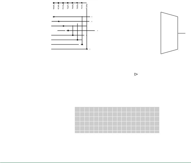
The simulation is shown in Figure 5.48. For clarity, digital data are present on the MUX inputs just before and after they are switched to the Y output. The output shows the channel data in sequence, starting with channel 0.
FIGURE 5.48
Simulation for an 8-bit Time-Division Multiplexer
SECTION 5.3 REVIEW PROBLEM
5.5What defines whether a multiplexer application is time-dependent or not? What additional component can be added to make a MUX application time-dependent?
5.4Demultiplexers
K E Y T E R M S
Demultiplexer A circuit that uses a binary decoder to direct a digital signal from
a single source to one of several destinations.
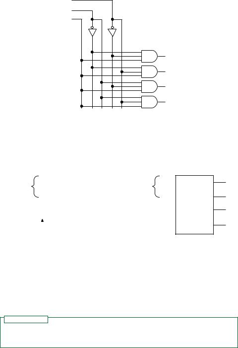
A demultiplexer performs the reverse function of a multiplexer. A multiplexer (MUX) directs one of several input signals to a single output; a demultiplexer (DMUX) directs a single input signal to one of several outputs. In both cases, the selected input or output is chosen by the state of an internal decoder.
Figure 5.49 shows the logic circuit for a 1-to-4 demultiplexer. Compare this to Figure 5.4, a 4-output decoder. This circuits are the same except that the active-LOW enable input has been changed to an active-HIGH data input. The circuit in Figure 5.49 could still be used as a decoder, except that its enable input would be active-HIGH.
198 C H A P T E R 5 • Combinational Logic Functions
S0
S1
D
Y0
Y1
Y2
Y3
FIGURE 5.49
4-bit Decoder/Demultiplexer
Each AND gate in the demultiplexer enables or inhibits the signal output according to the state of the select inputs, thus directing the data to one of the output lines. For instance, S1S0 10 directs incoming digital data to output Y2.
|
|
S1 |
Y0 |
|
|
|
S1 |
Y0 |
Binary |
|
Channel |
|
|||||
|
||||||||
|
|
|
|
|||||
input |
S0 |
|
|
select |
|
S0 |
|
|
|
|
Y1 |
|
|
|
Y1 |
||
|
|
|
|
|||||
|
|
|
|
|
|
|
||
Vcc |
|
Y2 |
|
|
|
|
Y2 |
|
|
|
|
|
|
||||
|
|
|
|
|
|
|
||
|
|
D |
Y3 |
|
Signal |
|
D |
Y3 |
|
|
|
|
|||||
|
|
|
|
|
|
|
|
|
|
a. Decoder |
|
|
b. Demultiplexer |
|
|||
FIGURE 5.50
Same Device Used as a Decoder or Demultiplexer
Figure 5.50 illustrates the use of a single device as either a decoder or a demultiplexer. In Figure 5.50a, input D is tied HIGH. When an output is selected by S1 and S0, it goes HIGH, acting as a decoder with active-HIGH outputs. In Figure 5.50b, D acts as a demultiplexer data input. The data are directed to the output selected by S1 and S0.
N O T E
Since a single device can be used either way, this implies that any of the VHDL binary decoder designs used in this chapter can also be used as demultiplexers.
A decoder/demultiplexer can have active-LOW outputs, but only if the D input is also active-LOW. This is important because the demultiplexer data must be inverted twice to retain its original logic values.
Demultiplexing a TDM Signal
In Example 5.10, we saw how a multiplexer could be used to send 8 digital channels across a single line, multiplexed over time. Obviously, such a system is not of much value if the signals cannot be sorted out at the receiving end. The received digital data must be demultiplexed and sent to their appropriate destinations.
|
|
|
|
|
|
|
|
|
|
|
5.4 |
• |
|
Demultiplexers |
199 |
||||||||||||||
|
The process is the reverse of multiplexing; data are sent to an output selected by a counter |
||||||||||||||||||||||||||||
|
at the DMUX select inputs. (We assume that the counters at the MUX and DMUX select in- |
||||||||||||||||||||||||||||
|
puts are somehow synchronized or possibly, if located close together, are the same counter.) |
||||||||||||||||||||||||||||
|
|
|
|
|
|
|
|
|
|
|
|
|
|
|
|
|
|
|
|||||||||||
EXAMPLE 5.11 |
Draw a demultiplexing circuit that will take the multiplexed output of the circuit in Fig- |
||||||||||||||||||||||||||||
|
ure 5.47 and distribute it to 8 different local telephone circuits. Write a VHDL file for the |
||||||||||||||||||||||||||||
|
demultiplexer and create a simulation file that shows its operation. Use active-LOW out- |
||||||||||||||||||||||||||||
|
puts for the demultiplexer. How does this affect the outputs when they are not transmit- |
||||||||||||||||||||||||||||
|
ting data? |
|
|
|
|
|
|
|
|
|
|
|
|
|
|
|
|
|
|
|
|
|
|
|
|
|
|
||
|
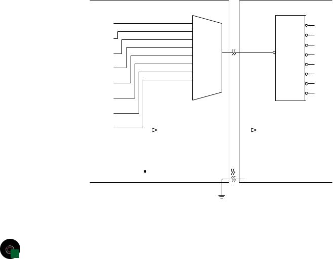
Solution Figure 5.51 shows the original multiplexing circuit connecting to the new de- |
||||||||||||||||||||||||||||
|
multiplexing circuit. The diagram indicates that the two sides of the circuit are separated |
||||||||||||||||||||||||||||
|
by some distance. The clock is shared between both sides of the circuit, but is generated |
||||||||||||||||||||||||||||
|
on the MUX side. Both sides share a common ground. Each side of the circuit has its own |
||||||||||||||||||||||||||||
|
3-bit counter. |
|
|
|
|
|
|
|
|
|
|
|
|
|
|
|
|
|
|
|
|
|
|
|
|
|
|
||
FIGURE 5.51 |
|
|
|
|
|
|
|
|
|
|
|
|
|
|
|
|
|
|
|
|
|
|
|
|
|
|
|
|
|
Example 5.11 |
|
|
|
|
|
|
|
MUX |
|
|
|
|
|
|
|
|
|
|
|
|
|
|
DMUX |
|
|
||||
Time-Division Multiplexing and |
|
|
|
|
|
|
|
|
|
|
|
|
|
|
|
|
|
|
|
|
|
|
|
||||||
|
|
|
|
|
|
|
|
|
|
|
|
|
|
|
|
|
|
|
|
|
|
|
|
|
|
|
|
|
|
CH0 |
|
|
|
|
D0 |
|
|
|
|
|
|
|
|
|
|
|
|
|
|
|
|
|
|
|
|
||||
Demultiplexing |
|
|
|
|
|
|
|
|
|
|
|
|
|
|
|
|
|
|
|
|
|
Y0 |
CH0 |
||||||
|
|
|
|
|
|
|
|
|
|
|
|
|
|
|
|
|
|
|
|
|
|
|
|
||||||
|
|
|
|
|
|
D1 |
|
|
|
|
|
|
|
|
|
|
|
|
|
|
|
|
|
Y1 |
|
||||
|
CH1 |
|
|
|
|
|
|
|
|
|
|
|
|
|
|
|
|
|
|
|
|
|
CH1 |
||||||
|
|
|
|
|
D2 |
|
|
|
|
|
|
|
|
|
|
|
|
|
|
|
|
|
|||||||
|
|
|
|
|
|
|
|
|
|
|
|
|
|
|
|
|
|
|
|
|
|
|
|||||||
|
|
|
|
|
|
|
|
|
|
|
|
|
|
|
|
|
|
|
|
|
Y2 |
|
|||||||
|
|
|
|
|
|
D3 |
Y |
|
|
|
|
|
|
|
|
|
D |
CH2 |
|||||||||||
|
CH2 |
|
|
|
D |
|
|
|
|
|
|
|
|
|
|
|
Y3 |
CH3 |
|||||||||||
|
|
|
|
|
|
4 |
|
|
|
|
|
|
|
|
|
|
|
|
|
|
|
|
|
|
|||||
|
|
|
|
|
|
|
|
|
|
|
|
|
|
|
|
|
|
|
|
|
|
|
|
|
|||||
|
|
|
|
|
|
|
|
|
|
|
|
|
|
|
|
|
|
|
|
|
|
|
|
|
|
Y |
|
|
|
|
CH3 |
|
|
|
|
D5 |
|
|
|
|
|
|
|
|
|
|
|
|
|
|
|
|
|
4 |
CH4 |
||||
|
|
|
|
|
|
|
|
|
|
|
|
|
|
|
|
|
|
|
|
|
|
|
|
||||||
|
|
|
|
|
|
D6 |
|
|
|
|
|
|
|
|
|
|
|
|
|
|
S2 |
Y5 |
CH5 |
||||||
|
|
|
|
|
|
|
|
|
|
|
|
|
|
|
|
|
|
|
|
||||||||||
|
CH4 |
|
|
|
D7 |
S |
|
|
|
|
|
|
|
|
|
|
|
|
|
S |
1 |
Y6 |
CH6 |
||||||
|
|
|
|
|
|
S2 S1 |
|
0 |
|
|
|
|
|
|
|
|
|
|
|
|
S0 |
Y7 |
CH7 |
||||||
|
CH5 |
|
|
|
|
|
|
|
|
|
|
|
|
|
|
|
|
|
|
||||||||||
|
|
CTR DIV 8 |
|
|
|
|
|
|
|
|
|
|
|
|
|
|
|
|
|
|
|
|
|
|
|
||||
|
|
|
|
|
|
|
|
|
|
|
|
|
|
|
|
|
|
|
|
|
|
|
|
|
|
|
|||
|
|
|
|
|
|
|
|
|
|
|
|
|
|
|
|
|
|
|
|
|
|
|
|
|
|
|
|||
|
CH6 |
|
Q |
|
|
|
|
|
|
|
|
|
|
Q |
2 |
Q |
1 |
Q |
0 |
|
|
|
|
|
|||||
|
|
|
|
2 |
|
|
|
|
|
|
|
|
|
|
|
|
|
|
|||||||||||
|
|
|
|
|
|
|
|
|
|
|
|
|
|
|
|
|
|
||||||||||||
|
|
|
|
|
|
|
|
|
|
|
|
|
|
|
|
|
|
|
|
|
|
|
|
|
|||||
|
|
|
|
|
|
|
|
|
|
|
|
|
|
|
|
|
|
|
|
|
|
|
|
|
|
|
|
|
|
|
CH7 |
|
|
Q1 |
|
|
|
|
|
|
|
|
|
|
|
|
|
|
|
|
|
|
|
|
|
|
|
|
|
|
|
|
|
Q0 |
|
|
|
|
|
|
|
|
|
|
|
|
|
|
|
|
|
|
|
|
|
|
|
||
|
|
|
|
|
|
|
|
|
|
|
|
|
|
|
|
|
|
|
|
|
|
|
|
|
|
|
|||
|
|
|
|
|
|
|
|
|
|
|
|
|
|
|
|
|
|
|
|
|
|
|
|
|
|||||
|
|
|
|
|
|
|
|
|
|
|
|
|
|
|
CTR DIV 8 |
|
|
|
|
||||||||||
|
CLOCK |
|
|
|
|
|
|
|
|
|
|
|
|
|
|
|
|
|
|
|
|
|
|
|
|
|
|
|
|
|
|
|
|
|
|
|
|
|
|
|
|
|
|
|
|
|
|
|
|
|
|
|
|
|
|
|
|
|
|
The VHDL code for the demultiplexer is as follows. (This is the same implementation as a 3-line-to-8-line decoder with an enable input.)
—— dmux8.vhd
—— 1-to-8 demultiplexer/decoder
dmux8.vhd
—— Decoder: set d to ‘0’; outputs are activated by
dmux8.scf
——binary combination of s.
——Demultiplexer: apply data stream to d; data directed to
——y output with subscript same as value of s.
——Outputs and d are active-LOW. DMUX data are inverted twice
——to keep them true.