

Digital design with CPLD applications and VHDL (R. Dueck, 2000)
.pdf110 C H A P T E R 3 • Boolean Algebra and Combinational Logic
3.25Use the rules of Boolean algebra to find the maximum SOP simplification of the function represented by the following truth table.
3.28Use the rules of Boolean algebra to find the maximum SOP simplification of the function represented by the following truth table.
A |
B |
C |
|
Y |
|
|
|
|
|
0 |
0 |
0 |
|
0 |
0 |
0 |
1 |
|
1 |
0 |
1 |
0 |
|
0 |
0 |
1 |
1 |
|
1 |
1 |
0 |
0 |
|
0 |
1 |
0 |
1 |
|
1 |
1 |
1 |
0 |
|
0 |
1 |
1 |
1 |
|
0 |
|
3.26Use the rules of Boolean algebra to find the maximum SOP simplification of the function represented by the following truth table.
A |
B |
C |
D |
|
Y |
|
|
|
|
|
|
0 |
0 |
0 |
0 |
|
0 |
0 |
0 |
0 |
1 |
|
0 |
0 |
0 |
1 |
0 |
|
0 |
0 |
0 |
1 |
1 |
|
0 |
0 |
1 |
0 |
0 |
|
1 |
0 |
1 |
0 |
1 |
|
1 |
0 |
1 |
1 |
0 |
|
0 |
0 |
1 |
1 |
1 |
|
0 |
1 |
0 |
0 |
0 |
|
0 |
1 |
0 |
0 |
1 |
|
1 |
1 |
0 |
1 |
0 |
|
0 |
1 |
0 |
1 |
1 |
|
1 |
1 |
1 |
0 |
0 |
|
1 |
1 |
1 |
0 |
1 |
|
1 |
1 |
1 |
1 |
0 |
|
0 |
1 |
1 |
1 |
1 |
|
1 |
|
3.27Use the rules of Boolean algebra to find the maximum SOP simplification of the function represented by the following truth table.
A |
B |
C |
D |
|
Y |
|
|
|
|
|
|
0 |
0 |
0 |
0 |
|
1 |
0 |
0 |
0 |
1 |
|
0 |
0 |
0 |
1 |
0 |
|
1 |
0 |
0 |
1 |
1 |
|
0 |
0 |
1 |
0 |
0 |
|
1 |
0 |
1 |
0 |
1 |
|
0 |
0 |
1 |
1 |
0 |
|
0 |
0 |
1 |
1 |
1 |
|
0 |
1 |
0 |
0 |
0 |
|
0 |
1 |
0 |
0 |
1 |
|
0 |
1 |
0 |
1 |
0 |
|
0 |
1 |
0 |
1 |
1 |
|
0 |
1 |
1 |
0 |
0 |
|
1 |
1 |
1 |
0 |
1 |
|
1 |
1 |
1 |
1 |
0 |
|
0 |
1 |
1 |
1 |
1 |
|
0 |
|
A |
B |
C |
D |
|
Y |
|
|
|
|
|
|
0 |
0 |
0 |
0 |
|
0 |
0 |
0 |
0 |
1 |
|
1 |
0 |
0 |
1 |
0 |
|
0 |
0 |
0 |
1 |
1 |
|
1 |
0 |
1 |
0 |
0 |
|
0 |
0 |
1 |
0 |
1 |
|
1 |
0 |
1 |
1 |
0 |
|
1 |
0 |
1 |
1 |
1 |
|
1 |
1 |
0 |
0 |
0 |
|
0 |
1 |
0 |
0 |
1 |
|
1 |
1 |
0 |
1 |
0 |
|
0 |
1 |
0 |
1 |
1 |
|
0 |
1 |
1 |
0 |
0 |
|
0 |
1 |
1 |
0 |
1 |
|
1 |
1 |
1 |
1 |
0 |
|
1 |
1 |
1 |
1 |
1 |
|
0 |
|
3.29Use the rules of Boolean algebra to find the maximum SOP simplification of the function represented by the following truth table.
A |
B |
C |
D |
|
Y |
|
|
|
|
|
|
0 |
0 |
0 |
0 |
|
1 |
0 |
0 |
0 |
1 |
|
0 |
0 |
0 |
1 |
0 |
|
0 |
0 |
0 |
1 |
1 |
|
1 |
0 |
1 |
0 |
0 |
|
1 |
0 |
1 |
0 |
1 |
|
0 |
0 |
1 |
1 |
0 |
|
0 |
0 |
1 |
1 |
1 |
|
0 |
1 |
0 |
0 |
0 |
|
1 |
1 |
0 |
0 |
1 |
|
0 |
1 |
0 |
1 |
0 |
|
1 |
1 |
0 |
1 |
1 |
|
1 |
1 |
1 |
0 |
0 |
|
1 |
1 |
1 |
0 |
1 |
|
0 |
1 |
1 |
1 |
0 |
|
1 |
1 |
1 |
1 |
1 |
|
1 |
|

3.30Use the rules of Boolean algebra to find the maximum SOP simplification of the function represented by the following truth table.
A |
B |
C |
D |
|
Y |
|
|
|
|
|
|
0 |
0 |
0 |
0 |
|
0 |
0 |
0 |
0 |
1 |
|
1 |
0 |
0 |
1 |
0 |
|
0 |
0 |
0 |
1 |
1 |
|
0 |
0 |
1 |
0 |
0 |
|
0 |
0 |
1 |
0 |
1 |
|
0 |
0 |
1 |
1 |
0 |
|
1 |
0 |
1 |
1 |
1 |
|
1 |
1 |
0 |
0 |
0 |
|
1 |
1 |
0 |
0 |
1 |
|
0 |
1 |
0 |
1 |
0 |
|
0 |
1 |
0 |
1 |
1 |
|
0 |
1 |
1 |
0 |
0 |
|
0 |
1 |
1 |
0 |
1 |
|
0 |
1 |
1 |
1 |
0 |
|
1 |
1 |
1 |
1 |
1 |
|
1 |
|
Section 3.4 Simplification by the Karnaugh Map Method
3.31Use the Karnaugh map method to find the maximum SOP
A B C D Y
0 |
0 |
0 |
0 |
0 |
0 |
0 |
0 |
1 |
0 |
0 |
0 |
1 |
0 |
0 |
0 |
0 |
1 |
1 |
1 |
0 |
1 |
0 |
0 |
0 |
0 |
1 |
0 |
1 |
1 |
0 |
1 |
1 |
0 |
0 |
0 |
1 |
1 |
1 |
1 |
1 |
0 |
0 |
0 |
0 |
1 |
0 |
0 |
1 |
0 |
1 |
0 |
1 |
0 |
0 |
1 |
0 |
1 |
1 |
1 |
1 |
1 |
0 |
0 |
0 |
1 |
1 |
0 |
1 |
1 |
1 |
1 |
1 |
0 |
0 |
1 |
1 |
1 |
1 |
1 |
simplification of the logic diagram in Figure 3.21.
3.32Use the Karnaugh map method to reduce the following Boolean expressions to their maximum SOP simplifications:
a.Y A B C A B C A B C
b.Y A B C A B C A B C A B C A B C
c.Y A B C A B C A B C A B C
d.Y A B C D A B C D A B C D A B C D
A B C D A B C D A B C D A B C D
A B C D
3.33Use the Karnaugh map method to reduce the Boolean expression represented by the following truth table to simplest SOP form.
3.34Use the Karnaugh map method to reduce the Boolean expression represented by the following truth table to simplest SOP form.
Problems 111
A |
B |
C |
D |
|
Y |
|
|
|
|
|
|
0 |
0 |
0 |
0 |
|
0 |
0 |
0 |
0 |
1 |
|
0 |
0 |
0 |
1 |
0 |
|
0 |
0 |
0 |
1 |
1 |
|
1 |
0 |
1 |
0 |
0 |
|
1 |
0 |
1 |
0 |
1 |
|
1 |
0 |
1 |
1 |
0 |
|
1 |
0 |
1 |
1 |
1 |
|
1 |
1 |
0 |
0 |
0 |
|
0 |
1 |
0 |
0 |
1 |
|
0 |
1 |
0 |
1 |
0 |
|
0 |
1 |
0 |
1 |
1 |
|
1 |
1 |
1 |
0 |
0 |
|
0 |
1 |
1 |
0 |
1 |
|
0 |
1 |
1 |
1 |
0 |
|
0 |
1 |
1 |
1 |
1 |
|
1 |
|
3.35Use the Karnaugh map method to reduce the Boolean expression represented by the following truth table to simplest SOP form.
A |
B |
C |
D |
|
Y |
|
|
|
|
|
|
0 |
0 |
0 |
0 |
|
0 |
0 |
0 |
0 |
1 |
|
1 |
0 |
0 |
1 |
0 |
|
0 |
0 |
0 |
1 |
1 |
|
1 |
0 |
1 |
0 |
0 |
|
0 |
0 |
1 |
0 |
1 |
|
1 |
0 |
1 |
1 |
0 |
|
0 |
0 |
1 |
1 |
1 |
|
1 |
1 |
0 |
0 |
0 |
|
1 |
1 |
0 |
0 |
1 |
|
0 |
1 |
0 |
1 |
0 |
|
0 |
1 |
0 |
1 |
1 |
|
0 |
1 |
1 |
0 |
0 |
|
0 |
1 |
1 |
0 |
1 |
|
1 |
1 |
1 |
1 |
0 |
|
0 |
1 |
1 |
1 |
1 |
|
1 |
|
3.36Use the Karnaugh map method to reduce the Boolean expression represented by the following truth table to simplest SOP form.
A |
B |
C |
D |
|
Y |
|
|
|
|
|
|
0 |
0 |
0 |
0 |
|
0 |
0 |
0 |
0 |
1 |
|
0 |
0 |
0 |
1 |
0 |
|
1 |
0 |
0 |
1 |
1 |
|
1 |
0 |
0 |
1 |
0 |
|
0 |
0 |
1 |
0 |
1 |
|
0 |
0 |
1 |
1 |
0 |
|
0 |
0 |
1 |
1 |
1 |
|
0 |
1 |
0 |
0 |
0 |
|
0 |
1 |
0 |
0 |
1 |
|
1 |
1 |
0 |
1 |
0 |
|
X |
1 |
0 |
1 |
1 |
|
X |
1 |
1 |
0 |
0 |
|
X |
1 |
1 |
0 |
1 |
|
X |
1 |
1 |
1 |
0 |
|
X |
1 |
1 |
1 |
1 |
|
X |
|
112 C H A P T E R 3 • Boolean Algebra and Combinational Logic
3.37Use the Karnaugh map method to reduce the Boolean expression represented by the following truth table to simplest SOP form.
A |
B |
C |
D |
|
Y |
|
|
|
|
|
|
0 |
0 |
0 |
0 |
|
1 |
0 |
0 |
0 |
1 |
|
1 |
0 |
0 |
1 |
0 |
|
1 |
0 |
0 |
1 |
1 |
|
1 |
0 |
1 |
0 |
0 |
|
0 |
0 |
1 |
0 |
1 |
|
0 |
0 |
1 |
1 |
0 |
|
1 |
0 |
1 |
1 |
1 |
|
0 |
1 |
0 |
0 |
0 |
|
1 |
1 |
0 |
0 |
1 |
|
0 |
1 |
0 |
1 |
0 |
|
1 |
1 |
0 |
1 |
1 |
|
0 |
1 |
1 |
0 |
0 |
|
0 |
1 |
1 |
0 |
1 |
|
1 |
1 |
1 |
1 |
0 |
|
1 |
1 |
1 |
1 |
1 |
|
0 |
|
3.38Use the Karnaugh map method to reduce the Boolean expression represented by the following truth table to simplest SOP form.
A |
B |
C |
D |
|
Y |
|
|
|
|
|
|
0 |
0 |
0 |
0 |
|
0 |
0 |
0 |
0 |
1 |
|
1 |
0 |
0 |
1 |
0 |
|
0 |
0 |
0 |
1 |
1 |
|
1 |
0 |
1 |
0 |
0 |
|
0 |
0 |
1 |
0 |
1 |
|
1 |
0 |
1 |
1 |
0 |
|
0 |
0 |
1 |
1 |
1 |
|
1 |
1 |
0 |
0 |
0 |
|
1 |
1 |
0 |
0 |
1 |
|
0 |
1 |
0 |
1 |
0 |
|
0 |
1 |
0 |
1 |
1 |
|
1 |
1 |
1 |
0 |
0 |
|
0 |
1 |
1 |
0 |
1 |
|
0 |
1 |
1 |
1 |
0 |
|
0 |
1 |
1 |
1 |
1 |
|
1 |
|
3.39Use the Karnaugh map method to reduce the Boolean expression represented by the following truth table to simplest SOP form.
A |
B |
C |
D |
|
Y |
|
|
|
|
|
|
0 |
0 |
0 |
0 |
|
1 |
0 |
0 |
0 |
1 |
|
1 |
0 |
0 |
1 |
0 |
|
0 |
0 |
0 |
1 |
1 |
|
0 |
0 |
1 |
0 |
0 |
|
1 |
0 |
1 |
0 |
1 |
|
1 |
0 |
1 |
1 |
0 |
|
0 |
0 |
1 |
1 |
1 |
|
1 |
1 |
0 |
0 |
0 |
|
0 |
1 |
0 |
0 |
1 |
|
0 |
1 |
0 |
1 |
0 |
|
1 |
1 |
0 |
1 |
1 |
|
1 |
1 |
1 |
0 |
0 |
|
0 |
1 |
1 |
0 |
1 |
|
1 |
1 |
1 |
1 |
0 |
|
1 |
1 |
1 |
1 |
1 |
|
1 |
|
3.40Use the Karnaugh map method to reduce the Boolean expression represented by the following truth table to simplest SOP form.
A |
B |
C |
D |
|
Y |
|
|
|
|
|
|
0 |
0 |
0 |
0 |
|
0 |
0 |
0 |
0 |
1 |
|
0 |
0 |
0 |
1 |
0 |
|
0 |
0 |
0 |
1 |
1 |
|
0 |
0 |
1 |
0 |
0 |
|
1 |
0 |
1 |
0 |
1 |
|
1 |
0 |
1 |
1 |
0 |
|
1 |
0 |
1 |
1 |
1 |
|
1 |
1 |
0 |
0 |
0 |
|
0 |
1 |
0 |
0 |
1 |
|
1 |
1 |
0 |
1 |
0 |
|
0 |
1 |
0 |
1 |
1 |
|
0 |
1 |
1 |
0 |
0 |
|
1 |
1 |
1 |
0 |
1 |
|
0 |
1 |
1 |
1 |
0 |
|
1 |
1 |
1 |
1 |
1 |
|
0 |
|
3.41Use the Karnaugh map method to reduce the Boolean expression represented by the following truth table to simplest SOP form.
A |
B |
C |
D |
|
Y |
|
|
|
|
|
|
0 |
0 |
0 |
0 |
|
1 |
0 |
0 |
0 |
1 |
|
0 |
0 |
0 |
1 |
0 |
|
1 |
0 |
0 |
1 |
1 |
|
1 |
0 |
1 |
0 |
0 |
|
0 |
0 |
1 |
0 |
1 |
|
0 |
0 |
1 |
1 |
0 |
|
0 |
0 |
1 |
1 |
1 |
|
1 |
1 |
0 |
0 |
0 |
|
0 |
1 |
0 |
0 |
1 |
|
0 |
1 |
0 |
1 |
0 |
|
1 |
1 |
0 |
1 |
1 |
|
1 |
1 |
1 |
0 |
0 |
|
0 |
1 |
1 |
0 |
1 |
|
0 |
1 |
1 |
1 |
0 |
|
0 |
1 |
1 |
1 |
1 |
|
1 |
|
3.42Use the Karnaugh map method to reduce the Boolean expression represented by the following truth table to simplest SOP form.
A |
B |
C |
D |
|
Y |
|
|
|
|
|
|
0 |
0 |
0 |
0 |
|
0 |
0 |
0 |
0 |
1 |
|
1 |
0 |
0 |
1 |
0 |
|
0 |
0 |
0 |
1 |
1 |
|
1 |
0 |
1 |
0 |
0 |
|
0 |
0 |
1 |
0 |
1 |
|
1 |
0 |
1 |
1 |
0 |
|
0 |
0 |
1 |
1 |
1 |
|
1 |
1 |
0 |
0 |
0 |
|
0 |
1 |
0 |
0 |
1 |
|
1 |
1 |
0 |
1 |
0 |
|
0 |
1 |
0 |
1 |
1 |
|
1 |
1 |
1 |
0 |
0 |
|
0 |
1 |
1 |
0 |
1 |
|
1 |
1 |
1 |
1 |
0 |
|
0 |
1 |
1 |
1 |
1 |
|
1 |
|
3.43Use the Karnaugh map method to reduce the Boolean expression represented by the following truth table to simplest SOP form.
A |
B |
C |
D |
|
Y |
|
|
|
|
|
|
0 |
0 |
0 |
0 |
|
1 |
0 |
0 |
0 |
1 |
|
1 |
0 |
0 |
1 |
0 |
|
1 |
0 |
0 |
1 |
1 |
|
1 |
0 |
1 |
0 |
0 |
|
0 |
0 |
1 |
0 |
1 |
|
0 |
0 |
1 |
1 |
0 |
|
1 |
0 |
1 |
1 |
1 |
|
1 |
1 |
0 |
0 |
0 |
|
1 |
1 |
0 |
0 |
1 |
|
1 |
1 |
0 |
1 |
0 |
|
1 |
1 |
0 |
1 |
1 |
|
1 |
1 |
1 |
0 |
0 |
|
0 |
1 |
1 |
0 |
1 |
|
0 |
1 |
1 |
1 |
0 |
|
0 |
1 |
1 |
1 |
1 |
|
0 |
|
Problems 113
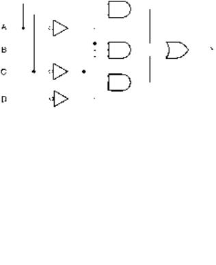
3.44The circuit in Figure 3.67 represents the maximum SOP simplification of a Boolean function.
Use a Karnaugh map to derive the circuit for the maximum POS
A |
B |
C |
D |
|
Y |
|
|
|
|
|
|
0 |
0 |
0 |
0 |
|
0 |
0 |
0 |
0 |
1 |
|
0 |
0 |
0 |
1 |
0 |
|
0 |
0 |
0 |
1 |
1 |
|
0 |
0 |
1 |
0 |
0 |
|
0 |
0 |
1 |
0 |
1 |
|
0 |
0 |
1 |
1 |
0 |
|
0 |
0 |
1 |
1 |
1 |
|
1 |
1 |
0 |
0 |
0 |
|
1 |
1 |
0 |
0 |
1 |
|
1 |
1 |
0 |
1 |
0 |
|
1 |
1 |
0 |
1 |
1 |
|
1 |
1 |
1 |
0 |
0 |
|
1 |
1 |
1 |
0 |
1 |
|
1 |
1 |
1 |
1 |
0 |
|
0 |
1 |
1 |
1 |
1 |
|
1 |
|
simplification.
FIGURE 3.67
Problem 3.44:
Logic Circuit
3.45Repeat Problem 3.44 for the circuit in Figure 3.68.
3.46 Refer to the BCD-to-2421 code converter developed in Example 3.22. Use a similar design procedure to develop
FIGURE 3.68
Problem 3.45:
Logic Circuit
the circuit of a 2421-to-BCD code converter.
3.47Excess-3 code is a decimal code that is generated by adding 0011 ( 310) to a BCD code. Table 3.18 shows

114 C H A P T E R 3 • Boolean Algebra and Combinational Logic
the relationship between a decimal digital code, natural BCD code, and Excess-3 code. Draw the circuit of a BCD-to-Excess-3 code converter, using the Karnaugh map method to simplify all Boolean expressions.
A N S W E R S T O S E C T I O N R E V I E W
3.48 Repeat Problem 3.47 for an Excess-3-to-BCD code converter.
Table 3.18 BCD and Excess-3 Code
Decimal |
|
BCD Code |
|
|
Excess-3 |
|
||
Equivalent |
D4 |
D3 |
D2 |
D1 |
E4 |
E3 |
E2 |
E1 |
|
|
|
|
|
|
|
|
|
0 |
0 |
0 |
0 |
0 |
0 |
0 |
1 |
1 |
1 |
0 |
0 |
0 |
1 |
0 |
1 |
0 |
0 |
2 |
0 |
0 |
1 |
0 |
0 |
1 |
0 |
1 |
3 |
0 |
0 |
1 |
1 |
0 |
1 |
1 |
0 |
4 |
0 |
1 |
0 |
0 |
0 |
1 |
1 |
1 |
5 |
0 |
1 |
0 |
1 |
1 |
0 |
0 |
0 |
6 |
0 |
1 |
1 |
0 |
1 |
0 |
0 |
1 |
7 |
0 |
1 |
1 |
1 |
1 |
0 |
1 |
0 |
8 |
1 |
0 |
0 |
0 |
1 |
0 |
1 |
1 |
9 |
1 |
0 |
0 |
1 |
1 |
1 |
0 |
0 |
|
|
|
|
|
|
|
|
|
P R O B L E M S
Section 3.1
3.1a Y ABC D b OUT (W X Y)Z
Section 3.2
A |
B |
C |
|
Y |
|
|
|
|
|
0 |
0 |
0 |
|
0 |
0 |
0 |
1 |
|
1 |
0 |
1 |
0 |
|
1 |
0 |
1 |
1 |
|
1 |
1 |
0 |
0 |
|
0 |
1 |
0 |
1 |
|
1 |
1 |
1 |
0 |
|
0 |
1 |
1 |
1 |
|
0 |
|
Section 3.3
3.3a SOP: Y A B C A B C
POS: Y (A B C)(A B C)(A B C) (A B C)(A B C)(A B C)
bSOP: Y A B C A B C A B C A B C
POS: Y (A B C )(A B C)(A B C ) (A B C )
Section 3.4 |
|
3.4a Y AC or Y A C |
3.4b Y AC D or |
|
Y A C D |
3.4c Y AB |
|
Section 3.5 |
|
3.5 SOP: Y AC BC |
POS: Y (A C )(B C) |
C H A P T E R 4
Introduction to PLDs and MAX PLUS II
O U T L I N E C H A P T E R O B J E C T I V E S
4.1What is a PLD? Upon successful completion of this chapter you will be able to:
4.2Programming PLDs • Describe some advantages of programmable logic over fixed-function
using MAX PLUS II |
logic. |
4.3Graphic Design File • Name some types of programmable logic devices (PLDs).
4.4 Compiling |
• Use Altera’s MAX PLUS II PLD Design Software to enter simple combi- |
MAX PLUS II Files |
national circuits using schematic capture. |
4.5Hierarchical Design • Use VHDL entity declarations, architecture bodies, and concurrent signal
4.6 |
Text Design File |
|
assignments to enter simple combinational circuits. |
|
(VHDL) |
• |
Create circuit symbols from schematic or VHDL designs and use them in |
4.7 |
Creating a Physical |
|
hierarchical designs for PLDs. |
|
Design |
• |
Assign device and pin numbers to schematic or VHDL designs and compile |
them for programming Altera MAX7000S or FLEX10K20 devices.
• Program Altera PLDs via a JTAG interface and a ByteBlaster Parallel Port Download Cable.
In the first three chapters of this book, we examined logic gates and Boolean algebra. These basic foundations of combinational circuitry, as well as the sequential logic circuits we will study in a later chapter, form the fundamental building blocks of many digi-
tal integrated circuits (ICs).
In the past, such digital ICs were fixed in their logic functions; it was not possible to change designs without changing the chips in a circuit. Programmable logic offers the digital circuit designer the possibility of changing design function even after it has been built. A programmable logic device (PLD) can be programmed, erased, and reprogrammed many times, allowing easier prototyping and design modification. (The industry marketing buzz often refers to “rapid prototyping” and “reduced time to market.”) The number of IC packages required to implement a design with one or more PLDs is often reduced, compared to a design fabricated using standard fixed-function ICs.
PLDs can be programmed from a personal computer (PC) or workstation running special software. This software is often associated with a set of programs that allow us to design circuits for various PLDs. MAX PLUS II, owned by Altera Corporation, is such a software package. MAX PLUS II allows us to enter PLD designs, either as schematics or in several hardware description languages (specialized computer languages for modeling and synthesizing digital hardware). A design can contain components that are in themselves complete digital circuits. MAX PLUS II converts the design information
115

116 C H A P T E R 4 • Introduction to PLDs and MAX+PLUS II
into a binary form that can be transferred into a PLD via a special interface connected to the parallel port of a PC. ■
4.1 What Is a PLD?
K E Y T E R M S
Programmable logic device (PLD) A digital integrated circuit that can be programmed by the user to implement any digital logic function.
Complex PLD (CPLD) A digital device consisting of several programmable sections with internal interconnections between the sections.
MAX PLUS II CPLD design and programming software owned by Altera Corporation.
Schematic capture A technique of entering CPLD design information by using a CAD (computer aided design) tool to draw a logic circuit as a schematic. The schematic can then be interpreted by design software to generate programming information for the CPLD.
Compile The process used by CPLD design software to interpret design information (such as a drawing or text file) and create required programming information for a CPLD.
One of the most far-reaching developments in digital electronics has been the introduction of programmable logic devices (PLDs). Prior to the development of PLDs, digital circuits were constructed in various scales of integrated circuit logic, such as small scale integration (SSI) and medium scale integration (MSI) devices. These devices contained logic gates and other digital circuits. The functions were determined at the time of manufacture and could not be changed. This necessitated the manufacture of a large number of device types, requiring shelves full of data books just to describe them. Also, if a designer wanted a device with a particular function that was not in a manufacturer’s list of offerings, he or she was forced to make a circuit that used multiple devices, some of which might contain functions neither wanted nor needed, thus wasting circuit board space and design time.
Programmable logic provides a solution to these problems. A PLD is supplied to the user with no logic function programmed in at all. It is up to the designer to make the PLD perform in whatever way a design requires; only those functions required by the design need be programmed. Since several functions can usually be combined in the design and programmed onto a single chip, the package count and required board space can be reduced as well. Also, if a design needs to be changed, a PLD can be reprogrammed with the new design information, often without removing it from the circuit.
PLD is a generic term. There is a wide variety of PLD types, including PAL (programmable array logic), GAL (generic array logic), EPLD (erasable PLD), CPLD (complex PLD), FPGA (field-programmable gate array), as well as several others. We will be focussing on CPLDs as a representative type of PLD. Although terminology varies somewhat throughout the industry, we will use the term CPLD to mean a device with several programmable sections that are connected internally. In effect, a CPLD is several interconnected PLDs on a single chip. This structure is not apparent to the user and doesn’t really concern us at this time, except as background information. We will look at the structure of PALs, GALs, and CPLDs in Chapter 8. We will use the term “PLD” when we are referring to a generic device and “CPLD” as a more specific type of PLD.
A complication in the use of programmable logic is that we must use specialized computer software to design and program our circuit. Initially, this might seem as though we are adding another level of work to the design, but when these computer techniques are mastered, it shortens the design process greatly and yields a level of flexibility not otherwise available.
|
|
|
|
|
|
|
|
|
|
|
|
|
|
|
|
|
|
|
|
|
|
|
|
|
|
|
|
|
4.1 • What Is a PLD? |
117 |
|||||||||||||||
|
|
|
|
|
|
Let’s look at two examples, comparing the use of SSI logic versus programmable |
|||||||||||||||||||||||||||||||||||||||
|
|
logic. |
|
|
|
|
|
|
|
|
|
|
|
|
|
|
|
|
|
|
|
|
|
|
|
|
|
||||||||||||||||||
|
|
|
|
|
|
|
|
|
|
|
|
|
|
|
|
|
|
|
|
|
|
|
|
|
|
|
|
|
|
|
|
|
|
|
|
|
|
|
|
|
|
|
|
|
|
EXAMPLE 4.1 |
|
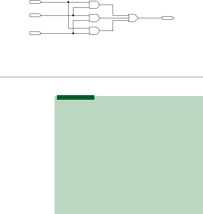
Figure 4.1 shows a majority vote circuit, as described in Problem 3.4 of Chapter 3. This cir- |
|||||||||||||||||||||||||||||||||||||||||||
|
|
cuit will produce a HIGH output when two out of three inputs are HIGH. Write the Boolean |
|||||||||||||||||||||||||||||||||||||||||||
|
|
equation for the circuit and state the minimum number and type of 74HC devices required |
|||||||||||||||||||||||||||||||||||||||||||
|
|
to build the circuit. How many packages would be required to build two such circuits? |
|
||||||||||||||||||||||||||||||||||||||||||
|
|
|
|
|
|
|
|
|
|
|
|
A |
|
|
|
|
|
|
|
|
|
|
|
|
|
|
|
|
|
|
|
|
|
|
|
|
|
|
|
|
|
|
|
|
|
|
|
|
|
|
|
|
|
|
|
|
|
|
|
|
|
|
|
|
|
|
|
|
|
|
|
|
|
|
|
|
|
|
|||||||||||||
|
|
|
|
|
|
|
|
|
|
|
|
B |
|
|
|
|
|
|
|
|
|
|
|
|
|
|
|
|
|
|
|
|
|
|
|
|
Y |
|
|||||||
|
|
|
|
|
|
|
|
|
|
|
|
|
|
|
|
|
|
|
|
|
|
|
|
|
|
|
|
|
|
|
|
|
|
|
|
|
|||||||||
|
|
|
|
|
|
|
|
|
|
|
|
|
|
|
|
|
|
|
|
|
|
|
|
|
|
|
|
|
|
|
|
|
|
|
|
|
|||||||||
|
|
|
|
|
|
|
|
|
|
|
|
|
|
|
|
|
|
|
|
|
|
|
|
|
|
||||||||||||||||||||
|
|
|
|
|
|
|
|
|
|
|
|
C |
|
|
|
|
|
|
|
|
|
|
|
|
|
|
|
|
|
|
|
|
|
|
|
|
|
||||||||
|
|
|
|
|
|
|
|
|
|
|
|
|
|
|
|
|
|
|
|
|
|
|
|
|
|
|
|
|
|
|
|
|
|
|
|
|
|
|
|
|
|
|
|
|
|
|
|
|
|
|
|
|
|
|
|
|
|
|
|
|
|
|
|
|
|
|
|
|
|
|
|
|
|
|
|
|
|
|
|
|
|
|
|
|
|
|
|
|
|
|
|
|
|
|
|
|
|
|
|
|
|
|
|
|
|
|
|
|
|
|
|
|
|
|
|
|
|
|
|
|
|
|
|
|
|
|
|
|
|
|
|
|
|
|
|
|
|
|
|
|
|
|
|
|
|
|
|
|
|
|
|
|
|
|
|
|
|
|
|
|
|
|
|
|
|
|
|
|
|
|
|
|
|
|
|
|
|
|
|
|
|
||
|
|
|
|
|
|
|
|
|
|
|
|
|
|
|
|
|
|
|
|
|
|
|
|
|
|
|
|
|
|
|
|
|
|||||||||||||
|
|
FIGURE 4.1 |
|
|
|
|
|
|
|
|
|
|
|
|
|
|
|
|
|
|
|
|
|
|
|
|
|
||||||||||||||||||
|
|
Majority Vote Circuit |
|
|
|
|
|
|
|
|
|
|
|
|
|
|
|
|
|
|
|
|
|
|
|
|
|
||||||||||||||||||
|
|
Solution |
|
|
|
|
|
|
|
|
|
|
|
|
|
|
|
|
|
|
|
|
|
|
|
|
|
||||||||||||||||||
|
|
Boolean equation: Y AB BC AC |
|
|
|
|
|
|
|
|
|
|
|
|
|
|
|
|
|
|
|
|
|
|
|
|
|
||||||||||||||||||
|
|
|
|
|
|
Figure 4.2 shows the 74HC devices required to build the majority vote circuit: one |
|||||||||||||||||||||||||||||||||||||||
|
|
74HC08A quad 2-input AND gate and one 74HC4075 triple 3-input OR gate. Figure 4.2 |
|||||||||||||||||||||||||||||||||||||||||||
|
|
also shows connections between the devices. Note that unused gate inputs are grounded |
|||||||||||||||||||||||||||||||||||||||||||
|
|
and unused outputs are left open. |
|
|
|
|
|
|
|
|
|
|
|
|
|
|
|
|
|
|
|
|
|
|
|
|
|
||||||||||||||||||
Vcc |
|
|
|
|
|
C |
|
|
|
|
|
|
|
|
|
|
|
|
|
|
|
|
|
|
|
|
|
|
|
|
|
||||||||||||||
|
|
|
|
|
|
|
|
|
|
|
|
|
|
|
|
Vcc |
|
|
|
|
|
|
|
|
|
|
|
|
|
|
|
|
|
|
|
|
|
|
|
|
|
||||
|
|
|
|
|
|
|
|
|
|
|
|
|
|
|
|
|
|
|
|
|
|
|
|
|
|
|
|
|
|
|
|
|
|
|
|
|
|
|
|
|
|||||
|
|
|
|
|
|
|
|
|
|
|
|
|
|
|
|
|
|
|
|
|
|
|
|
|
|
|
|
|
|
|
|
|
|
|
|
|
|
|
|
|
|||||
|
|
|
|
|
|
|
|
|
|
|
|
|
|
|
|
|
|
|
|
|
|
|
|
|
|
|
|
|
|
|
|
|
|
|
|
|
|
|
|
|
|
|
|
|
|
|
|
|
|
|
|
|
|
|
|
|
|
|
|
|
|
|
|
|
|
|
|
|
|
|
|
|
|
|
|
|
|
|
|
|
|
|
|
|
|
|
|
|
|
|
|
|
|
|
|
|
|
|
|
|
|
|
|
|
|
|
|
|
|
|
|
|
|
|
|
|
|
|
|
|
|
|
|
|
|
|
|
|
|
|
|
|
|
|
|
|
|
|
|
|
|
|
|
|
|
|
|
|
|
|
|
|
|
|
|
|
|
|
|
|
|
|
|
|
|
|
|
|
|
|
|
|
|
|
|
|
|
|
|
|
|
|
|
|
|
|
|
|
|
|
|
|
|
|
|
|
|
|
|
|
|
|
|
|
|
|
|
|
|
|
|
|
|
|
|
|
|
|
|
|
|
|
|
|
|
|
|
|
|
|
|
|
|
|
|
|
|
|
|
|
|
|
|
|
|
|
|
|
|
|
|
|
|
|
|
|
|
|
|
|
|
|
|
|
|
|
|
|
|
|
|
|
|
|
|
|
|
|
|
|
|
|
|
|
|
|
|
|
|
|
|
|
|
|
|
|
|
|
|
|
|
|
|
|
|
|
|
|
|
|
|
|
|
|
|
|
|
|
|
|
|
|
|
|
|
|
|
|
|
|
|
|
|
|
|
|
|
|
|
|
|
|
|
|
|
|
|
|
|
|
|
|
|
|
|
|
|
|
|
|
|
|
|
|
|
|
|
|
|
|
|
|
|
|
|
|
|
|
|
|
|
|
|
|
|
|
|
|
|
|
|
|
|
|
|
|
|
|
|
|
|
|
|
|
|
|
|
|
|
|
|
|
|
|
|
|
|
|
|
|
|
|
|
|
|
|
|
|
|
|
|
|
|
|
|
|
|
|
|
|
|
|
|
|
|
|
|
|
|
|
|
|
|
|
|
|
|
|
|
|
|
|
|
|
|
|
|
|
|
|
|
|
|
|
|
|
|
|
|
|
|
|
|
|
|
|
|
|
|
|
|
|
|
|
|
|
|
|
|
|
|
|
|
|
|
|
|
|
|
|
|
|
|
|
|
|
|
|
|
|
|
|
|
|
|
|
|
|
|
|
|
|
|
|
|
|
|
|
|
|
|
|
|
|
|
|
|
|
|
|
|
|
|
|
|
|
|
|
|
|
|
|
|
|
|
|
|
|
|
|
|
|
|
|
|
|
|
|
|
|
|
|
|
|
|
|
|
|
|
|
|
|
|
|
|
|
|
|
|
|
|
|
|
|
|
|
|
|
|
|
|
|
|
|
|
|
|
|
|
|
|
|
|
|
|
|
|
|
|
|
|
|
|
|
|
|
|
|
|
|
|
|
|
|
|
|
|
|
|
|
|
|
|
|
|
|
|
|
|
|
|
|
|
|
|
|
|
|
|
|
|
|
|
|
|
|
|
|
|
|
|
|
|
|
|
|
|
|
|
A |
B |
|
|
|
Y |
||
FIGURE 4.2 |
74HC08A |
|
|
|
|
|
74HC4075 |
|
|
|
|
|
|||
|
|
|
|
|
|||
|
|
|
|
|
|
|
|
74HC Devices Required to Build a Majority Vote Circuit |
|
|
|
|
|||
|
Two majority vote circuits would require 6 ANDs and two ORs. This requires one |
||||||
|
more 74HC08A package. |
|
|
|
|
||
|
|
||||||
EXAMPLE 4.2 |
Show how a CPLD can be programmed with a majority vote function, using a schematic |
||||||
|
capture tool. State how many CPLDs would be required to build two majority vote |
||||||
|
circuits. |
|
|
|
|
||
Solution A CPLD can be programmed by entering the schematic directly, using PLD programming software, such as Altera Corporation’s MAX PLUS II. Figure 4.3 shows the circuit as entered in a MAX PLUS II Graphic Design File.
118 C H A P T E R 4 • Introduction to PLDs and MAX+PLUS II
INPUT |
AND2 |
|
|
A |
|
|
|
INPUT |
AND2 |
OR3 |
|
OUTPUT |
|||
B |
|
||
|
|
Y
AND2
INPUT
C
FIGURE 4.3
MAX PLUS II Graphic Design File of a Majority Vote Circuit
The design can be compiled by MAX PLUS II to create the information required to program the CPLD with the majority vote circuit. If a second copy of the circuit is required, the first circuit can easily be duplicated by a Copy and Paste procedure. The two
circuits can than be compiled together and used to program a single CPLD.
4.2 Programming PLDs using MAX PLUS II
K E Y T E R M S
Design entry The process of using software tools to describe the design requirements of a PLD. Design entry can be done by entering a schematic or a text file that describes the required digital function.
Fitting Assigning internal PLD circuitry, as well as input and output pins, for a
PLD design.
Simulation Verifying design function by specifying a set of inputs and observing the resultant outputs. Simulation is generally shown as a series of input and output waveforms.
Programming Transferring design information from the computer running PLD design software to the actual PLD chip.
Download Program a PLD from a computer running PLD design and programming software.
Software tools Specialized computer programs used to perform specific functions such as design entry, compiling, fitting, and so on. (Sometimes just called “tools.”)
Suite (of software tools) A related collection of tools for performing specific tasks. MAX PLUS II is a suite of tools for designing and programming digital functions in a PLD.
Target device The specific PLD for which a digital design is intended.
Altera UP-1 board A circuit board, part ofAltera’s University Program Design
Laboratory Package, containing two CPLDs and a number of input and output devices.
In order to take a digital design from the idea stage to the programmed silicon chip, we must go through a series of steps known as the PLD Design Cycle. These include design entry, simulation, compiling, fitting, and programming. All steps require the use of PLD software, such as Altera’s MAX PLUS II, a suite of software tools, to perform the various tasks of the design cycle. Some tasks, such as design entry, require a great deal of attention; others, such as fitting a design to a specified CPLD, are done automatically during the compiling process.
We will be using MAX PLUS II as a vehicle for learning the concepts that relate to PLD design and programming. The target devices for our designs will be two Altera CPLDs, both installed on a circuit board available from Altera called the University Pro-

4.2 • Programming PLDs Using MAX+PLUS II |
119 |
gram Design Laboratory Package. We will generally refer to this board, shown in Figure 4.4, as the Altera UP-1 board.
FIGURE 4.4
Altera UP-1 Board
Figure 4.5 shows photos of the two CPLDs used in the Altera UP-1 Board. Figure 4.5a shows the CPLD from the MAX7000S family, part number EPM7128SLC84-7. Figure 4.5b shows the CPLD from Altera’s FLEX10K series, part number EPF10K20RC240-4. These part numbers are meaningful and will be discussed in detail in Chapter 8.
FIGURE 4.5
Altera MAX7000S and FLEX10K CPLDs
In the remaining part of this chapter, we will learn how to enter a design in MAX PLUS II in both graphical and text format, how to compile the design, and how to download it into either one of the CPLDs on the Altera UP-1 circuit board.
Treat this design example as a tutorial in MAX PLUS II. Follow along with all the steps on your own computer to get the maximum benefit from the chapter. If you do not have access to the Altera UP-1 board or an equivalent, you can still follow through most of the steps.