

Digital design with CPLD applications and VHDL (R. Dueck, 2000)
.pdf60 C H A P T E R 3 • Boolean Algebra and Combinational Logic
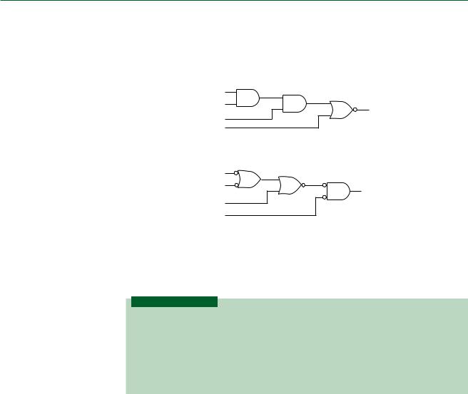
Figure 3.4 shows two logic diagrams, one whose Boolean expression requires parentheses and one that does not.
A
B
C
A
B
C
FIGURE 3.4
Order of Precedence
AB
AB AC
AC
a. No parentheses required (AND, then OR)
A B
(A B) (A B C)
A B C
b. Parentheses required (OR, then AND)
The AND functions in Figure 3.4a are evaluated first, eliminating the need for parentheses in the output expression. The expression for Figure 3.4b requires parentheses since the ORs are evaluated first.
EXAMPLE 3.3
FIGURE 3.5
Example 3.5
Order of Precedence
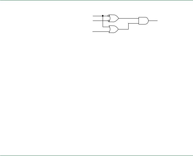
Write the Boolean expression for the logic diagrams in Figure 3.5.
A
1
B
3 Y
2
C
a.
P
1
Q
3 S
2
R
b.
Solution Examine the output of each gate and combine the resultant terms as required.
Figure 3.5a: Gate 1: A B
Gate 2: B C
Gate 3: Y Gate 1 Gate2 A B B C
Figure 3.5b: Gate 1: P Q P Q
Gate 2: Q R
Gate 3: S Gate1 Gate2 (P Q)(Q R) (P Q)(Q R)
3.1 • Boolean Expressions, Logic Diagrams and Truth Tables |
61 |
Note that when two bubbles touch, they cancel out, as in the doubly inverted P input or the connection between the outputs of gates 1 and 2 and the inputs of gate 3. In the re-
sultant Boolean expression, bars of the same length cancel; bars of unequal length do not.
SECTION 3.1A REVIEW PROBLEM
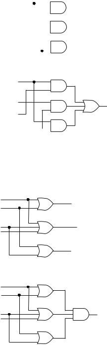
3.1Write the Boolean expression for the logic diagrams in Figure 3.6, paying attention to the rules of order of precedence.
A
B
Y
C
D
a.
W
X
OUT
Y
Z
b.
FIGURE 3.6
Section Review Problem 3.1
Logic Diagrams from Boolean Expressions
K E Y T E R M S
Levels of gating The number of gates through which a signal must pass from input to output of a logic gate network.
Double-rail inputs Boolean input variables that are available to a circuit in both
true and complement form.
Synthesis The process of creating a logic circuit from a description such as a Boolean equation or truth table.
We can derive a logic diagram from a Boolean expression by applying the order of precedence rules. We examine an expression to create the first level of gating from the circuit inputs, then combine the output functions of the first level in the second level gates, and so forth. Input inverters are often not counted as a gating level, as we usually assume that each variable is available in both true (noninverted) and complement (inverted) form. When input variables are available to a circuit in true and complement form, we refer to them as double-rail inputs.
The first level usually will be AND gates if no parentheses are present, OR gates if parentheses are used. (Not always, however; parentheses merely tell us which functions to synthesize first.) Although we will try to eliminate bars over groups of variables by use of DeMorgan’s theorems and the bubble-to-bubble convention, we should recognize that a bar over a group of variables is the same as having those variables in parentheses.
Let us examine the Boolean expression Y AC BD AD. Order of precedence tells us that we synthesize the AND functions first. This yields three 2-input AND gates, with outputs AC, BD, and AD, as shown in Figure 3.7a. In the next step, we combine these AND functions in a 3-input OR gate, as shown in Figure 3.7b.
62 |
C H A P T E R |
3 • Boolean Algebra and Combinational Logic |
||||||||
FIGURE 3.7 |
A |
|
|
|
|
|
|
AC |
||
|
|
|
|
|
|
|||||
Logic Diagram for |
|
|
|
|
|
|
|
|
|
|
Y AC BD AD |
|
|
|
|
|
|
|
|
BD |
|
|
|
B |
|
|
|
|
|
|
|
|
|
|
|
|
|
|
|
|
|
||
|
|
C |
|
|
|
|
|
|
|
|
|
|
|
|
|
|
|
|
|
AD |
|
|
|
|
|
|
|
|
|
|
||
|
|
|
|
|
|
|
|
|
||
|
|
|
|
|
|
|
|
|
|
|
|
|
|
|
|
|
|
|
|
||
|
|
D |
|
|
|
|
|
|
|
|
|
|
|
|
|
|
|
|
|||
|
|
|
a. ANDs first |
|||||||
|
|
|
|
|
||||||
A
B
Y AC BD AD
C
D
b.Combine ANDs in an OR gate
FIGURE 3.8
Logic Diagram for Y (A B) (A C D) (B C)
When the expression has OR functions in parentheses, we synthesize the ORs first, as for the expression Y (A B)(A C D)(B C). Figure 3.8 shows this process. In the first step, we synthesize three OR gates for the terms (A B), (A C D), and (B C). We then combine these terms in a 3-input AND gate.
(A B)
A
B
(A C D)
C D
(B C)
|
a. ORs first |
|
A |
|
|
B |
|
|
C |
Y (A B)(A C D)(B C) |
|
D |
||
|
|
b. Combine ORs in an AND gate |
|
|
EXAMPLE 3.4 |
Synthesize the logic diagrams for the following Boolean expressions: |
|
1. P QRS ST |
|
2. X (W Z Y)V (W V)Y |
Solution
1.Recall that a bar over two variables acts like parentheses. Thus the QRS term is synthe-
sized from a NAND, then an AND, as shown in Figure 3.9a. Also shown is the second AND term, ST.
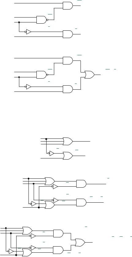
FIGURE 3.9
Example 3.4
Logic Diagram of
P QRS ST
FIGURE 3.10
Example 3.4
Logic Diagram for X
(W Z Y)V (W V)Y
3.1 • Boolean Expressions, Logic Diagrams and Truth Tables |
63 |
Figure 3.9b shows the terms combined in an OR gate.
Q |
QRS |
|
R |
RS |
|
S |
|
|
|
S |
|
|
ST |
|
T |
|
|
|
a. Combine inputs (NAND, then AND) |
|
Q |
QRS |
|
R |
RS |
P QRS ST |
S |
|
|
S
ST
T
b.First and second level gates combined in and OR
2.Figure 3.10 shows the synthesis of the second logic diagram in three stages. Figure 3.10a shows how the circuit inputs are first combined in two OR gates. We do this first because the ORs are in parentheses. In Figure 3.10b, each of these functions is combined in an AND gate, according to the normal order of precedence. The AND outputs are combined in a final OR function, as shown in Figure 3.10c.
W |
|
W Z Y |
Z |
|
|
Y |
|
|
|
W |
W V |
|
|
|
V |
|
|
|
a. ORs first (parentheses) |
|
W |
W Z Y |
Z |
|
Y |
V |
|
Y |
W |
W V |
V |
|
(W Z Y)V
(W V)Y
b. Combine with ANDs (order of precedence)
W |
W Z Y |
Z |
|
Y |
V |
|
Y |
W |
W V |
V |
|
(W Z Y)V
X (W X Y)V (W V)Y
(W V)Y
c. Find output (OR)
64 |
C H A P T E R |
3 • Boolean Algebra and Combinational Logic |
|
|
|
|
|
|
|
|
|
|
|
|
|
|
|
|
|
|
|
|
|
|
|
|
|||||||||||||||||||||||||||||||||||||
|
|
|
|
|
|
|
|
|
|
|
|
|
|
|
|
|
|
|
|
|
|
|
|
|
|
|
|
|
|
|
|
|
|
|
|
|
|
|
|
|
|
|
|
|
|
|
|
|
|
|
|
|
|
|
|
|
|
|
|
|
|||
|
EXAMPLE 3.5 |
Use DeMorgan’s theorem to modify the Boolean equation in part 1 of Example 3.4 so that |
|||||||||||||||||||||||||||||||||||||||||||||||||||||||||||||
|
|
there is no bar over any group of variables. Redraw Figure 3.9b to reflect the change. |
|||||||||||||||||||||||||||||||||||||||||||||||||||||||||||||
|
|
Solution |
|
|
|
|
|
|
|
|
|
|
|
|
|
|
|
|
|
|
|
|
|
|
|
|
|
|
|
|
|
|
|
|
|
|
|
|
|
|
|
|
|
|
|
|
|
|
|
|
|
|
|
|
|
|
|
|
|
|
|
|
|
|
|
|
|
|
|
|
|
|
P QRS ST Q(R S) ST |
||||||||||||||||||||||||||||||||||||||||||||||||||||||
|
|
Figure 3.11a shows the modified logic diagram. The levels of gating could be further |
|||||||||||||||||||||||||||||||||||||||||||||||||||||||||||||
|
|
reduced from three to two (not counting input inverters) by “multiplying through” the |
|||||||||||||||||||||||||||||||||||||||||||||||||||||||||||||
|
|
parentheses to yield the expression: |
|
|
|
|
|
|
|
|
|
|
|
|
|
|
|
|
|
|
|
|
|
|
|
|
|||||||||||||||||||||||||||||||||||||
|
|
|
|
|
|
|
|
|
|
|
|
|
P QR QS ST |
|
|
|
|
|
|
|
|
|
|
|
|
|
|
|
|
|
|
|
|
|
|
|
|
||||||||||||||||||||||||||
|
|
Figure 3.11b shows the logic diagram for this form. We will examine this simplifica- |
|||||||||||||||||||||||||||||||||||||||||||||||||||||||||||||
|
|
tion procedure more formally in a later section of this chapter. |
|||||||||||||||||||||||||||||||||||||||||||||||||||||||||||||
|
|
Q |
|
|
|
|
|
|
|
|
|
|
|
|
|
|
|
|
|
|
|
|
|
|
|
|
|
|
|
|
|
|
|
|
|
|
|
|
|
|
|
|
|
|
|
|
|
|
|
|
|
|
|
|
|
|
|
|
|
|
|
|
|
|
|
|
|
|
|
|
|
|
|
|
|
|
|
|
|
|
|
|
|
|
|
|
|
|
|
|
Q(R |
|
S) |
|
|
|
|
|
|
|
|
|
|
|
|
|
|
|
|
|
|
|
|
|
|
|
|
||||||||||
|
|
R |
|
|
|
|
|
|
|
|
|
|
|
|
|
|
|
|
|
|
|
|
|
|
|
|
|
|
|
|
|
|
|
|
|
|
|
|
|
|
|
|
|
|
|
|
|
|
|
|
|
|
|
|
|
||||||||
|
|
|
|
|
|
|
|
|
|
(R |
|
S) |
|
|
|
|
|
|
|
|
|
|
|
|
|
|
|
|
|
|
|
|
|
|
|
|
|
|
|
|
|
|
|
|
|
|
|
|
|
|
|
|
|||||||||||
|
|
|
|
|
|
|
|
|
|
|
|
|
|
|
|
|
|
|
|
|
|
|
|
|
|
|
|
|
|
|
|
|
|
|
|
|
|
|
|
|
|
|
|
|
|
|
|
|
|||||||||||||||
|
|
S |
|
|
|
|
|
|
|
|
|
|
|
|
|
|
|
|
|
|
|
|
|
|
|
|
|
|
|
|
|
|
|
|
|
|
|
|
|
|
|
|
|
|
|
|
|
|
|
|
|
|
|
|
|
|
|
|
|
|
|
|
|
|
|
|
|
|
|
|
|
|
|
|
|
|
|
|
|
|
|
|
|
|
|
|
|
|
|
|
|
|
|
|
|
|
|
|
|
|
|
|
|
|
|
|
|
|
|
|
|
|
|
|
P Q(R |
|
S) ST |
||||||||||
|
|
|
|
|
|
|
|
|
|
|
|
|
|
|
|
|
|
|
|
|
|
|
|
|
|
|
|
|
|
|
|
|
|
|
|
|
|
|
|
|
|
|
|
|
|
|
|
|
|
||||||||||||||
|
|
|
|
|
|
|
|
|
|
|
|
|
|
|
|
|
|
|
|
|
|
|
|
|
|
|
|
|
|
|
|
|
|
|
|
|
|
|
|
|
|
|
|
|
|
|
|
|
|
|
|
|
|
|
|
|
|
|
|
|
|
|
|
|
|
|
|
|
|
|
|
|
|
|
|
|
|
|
|
|
|
|
|
|
|
|
|
|
|
|
|
|
|
|
|
|
|
|
|
|
|
|
|
|
|
|
|
|
|
|
|
|
|
|
|
|
|
|
|
|
|||||||
|
|
|
|
|
|
|
|
|
|
|
|
|
|
S |
|
|
|
|
|
|
|
|
|
|
|
|
|
|
|
|
|
|
|
|
|
|
|
|
|
|
|
|
|
|
|
|
|
|
|
|
|
|
|
|
|
|
|
|
|||||
|
|
T |
|
|
|
|
|
|
|
|
|
|
|
|
|
|
|
|
|
|
|
|
|
|
|
|
ST |
|
|
|
|
|
|
|
|
|
|
|
|
|
|
|
|
|
|
|
|
|
|
|
|
|
|
|
|
|
|
|
|||||
|
|
|
|
|
|
|
|
|
|
|
|
|
|
|
|
|
|
|
|
|
|
|
|
|
|
|
|
|
|
|
|
|
|
|
|
|
|
|
|
|
|
|
|
|
|
|
|
|
|
|
|
|
|
||||||||||
|
|
|
|
|
|
|
|
|
|
|
|
|
|
|
|
|
|
|
|
|
|
|
|
|
|
|
|
|
|
|
|
|
|
|
|
|
|
|
|
|
|
|
|
|
|
|
|
|
|
|
|
|
|
|
|
|
|
|
|
|
|
|
|
|
|
|
|
|
|
|
|
|
|
|
|
|
|
|
|
|
|
|
|
|
|
|
|
|
|
|
|
|
|
|
|
|
|
|
|
|
|
|
|
|
|
|
|
|
|
|
|
|
|
|
|
|
|
|
|
|
|
|
|
|
|
|
|
|
|
|
|
|
|
|
|
|
|
|
|
|
|
|
|
|
|
|
|
|
|
|
|
|
|
|
|
|
|
|
|
|
|
|
|
|
|
|
|
|
|
|
|
|
|
|
|
|
|
|
|
|
|
|
|
|
|
|
|
|
|
|
|
|
|
|
|
|
|
|
|
|
|
|
|
|
|
|
|
|
|
|
|
|
|
|
|
|
|
|
|
|
|
|
|
||||||||||||||||||||||||||||||||
|
|
|
|
|
|
|
|
|
a. Logic diagram of P Q(R |
S) ST |
|||||||||||||||||||||||||||||||||||||||||||||||||||||
|
|
|
|
|
|
|
|
|
|
|
|
|
|
|
|
|
|
|
|
|
|
|
|
|
|
|
|
|
|
|
|
|
|
|
|
|
|
|
|
|
|
|
|
|
|
|
|
|
|
|
|
|
|||||||||||
|
|
|
Q |
|
|
|
|
|
|
|
|
|
|
|
|
|
|
|
QR |
|
|
|
|
|
|
|
|
|
|
|
|
|
|
|
|
|
|
|
|
|
|
|
|
|
|
|
|||||||||||||||||
|
|
|
|
|
|
|
|
|
|
|
|
|
|
|
|
|
|
|
|
|
|
|
|
|
|
|
|
|
|
|
|
|
|
|
|
|
|
|
|
|
|
|
|
|
|
|
|
|
|
|
|
|
|
|
|
|
|
|
|
||||
|
|
|
R |
|
|
|
|
|
|
|
|
|
|
|
|
|
|
|
|
|
|
|
|
|
|
|
|
|
|
|
|
|
|
|
|
|
|
|
|
|
|
|
|
|
|
|
|
|
|
|
|
|
|
|
|
|
|
|
|
|
|||
|
|
|
|
|
|
|
|
|
|
|
|
|
|
|
|
|
|
|
|
|
|
|
|
|
|
|
|
|
|
|
|
|
|
|
|
|
|
|
|
|
|
|
|
|
|
|
|
|
|
|
|
|
|
|
|
|
|
|
|
||||
|
|
|
|
|
|
|
|
|
|
|
|
|
|
|
|
|
|
|
|
|
|
|
|
|
|
|
|
|
|
|
|
|
|
|
|
|
|
|
|
P QR QS ST |
|||||||||||||||||||||||
|
|
|
S |
|
|
|
|
|
|
|
|
|
|
|
|
|
|
|
QS |
|
|
|
|
|
|
|
|
|
|
|
|
|
|
|
|
||||||||||||||||||||||||||||
|
|
|
|
|
|
|
|
|
|
|
|
|
|
|
|
|
|
|
|
|
|
|
|
|
|
|
|
|
|
|
|
||||||||||||||||||||||||||||||||
|
|
|
|
|
|
|
|
|
|
|
|
|
|
|
|
|
|
|
|
|
|
|
|
|
|
|
|
|
|
|
|
|
|
|
|
|
|
|
|
|
|
|
|
|
|
|
|
|
|
|
|
|
|
|
|
|
|
|
|
||||
|
|
|
|
|
|
|
|
|
|
|
|
|
|
|
|
|
|
|
|
|
|
|
|
|
|
|
|
|
|
|
|
|
|
|
|
|
|
|
|
|
|
|
|
|
|
|
|
|
|
|
|
|
|
|
|
|
|
|
|
||||
|
|
|
T |
|
|
|
|
|
|
|
|
|
|
|
|
|
|
|
|
|
|
ST |
|
|
|
|
|
|
|
|
|
|
|
|
|
|
|
|
|
|
|
|
|
|
|
|
|
|
|
|
|
|
|
|
|
|
|
|
|||||
|
|
|
|
|
|
|
|
|
|
|
|
|
|
|
|
|
|
|
|
|
|
|
|
|
|
|
|
|
|
|
|
|
|
|
|
|
|
|
|
|
|
|
|
|
|
|
|
|
|
|
|
|
|
|
|
||||||||
|
|
|
|
|
|
|
|
|
|
|
|
|
|
|
|
|
|
|
|
|
|
|
|
|
|
|
|
|
|
|
|
|
|
|
|
|
|
|
|
|
|
|
|
|
|
|
|
|
|
|
|
|
|
|
|
|
|
|
|
|
|||
|
|
|
|
|
|
|
|
|
|
|
|
|
|
|
|
|
|
|
|
|
|
|
|
|
|
|
|
|
|
|
|
|
|
|
|
|
|
|
|
|
|
|
|
|
|
|
|
|
|
|
|
|
|
|
|
|
|
|
|
|
|||
|
|
|
|
|
|
|
|
|
|
|
|
|
|
|
|
|
|
|
|
|
|
|
|
|
|
|
|
|
|
|
|
|
|
|
|
|
|
|
|
|
|
|
|
|
|
|
|
|
|
|
|
|
|
|
|
|
|
|
|
|
|||
|
|
|
|
|
|
|
|
|
|
|
|
|
|
|
|
|
|
|
|
|
|
|
|
|
|
|
|
|
|
|
|
|
|
|
|
|
|
|
|
|
|
|
|
|
|
|
|
|
|
|
|
|
|||||||||||
|
|
|
|
|
|
|
|
|
b. Logic diagram of P QR QS |
|
ST |
||||||||||||||||||||||||||||||||||||||||||||||||||||
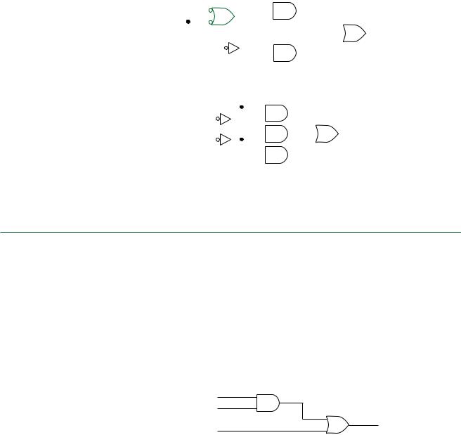
FIGURE 3.11
Example 3.5: Reworking Figure 3.9b
FIGURE 3.12
Logic Diagram for AB C
Truth Tables from Logic Diagrams or Boolean Expressions
There are two basic ways to find a truth table from a logic diagram. We can examine the output of each gate in the circuit and develop its truth table. We then use our knowledge of gate properties to combine these intermediate truth tables into the final output truth table. Alternatively, we can develop a Boolean expression for the logic diagram and by examining the expression fill in the truth table in a single step. The former method is more thorough and probably easier to understand when you are learning the technique. The latter method is more efficient, but requires some practice and experience. We will look at both.
Examine the logic diagram in Figure 3.12. Since there are three binary inputs, there will be eight ways those inputs can be combined. Thus, we start by making an 8-line truth table, as in Table 3.1.
A |
AB |
|
|
B |
|
AB C
C
3.1 • Boolean Expressions, Logic Diagrams and Truth Tables |
65 |
The OR gate output will describe the function of the whole circuit. In order to assess the OR function, we must first evaluate the AND output. We add a column to the truth table for the AND gate and look for the lines in the table where both A AND B equal logic 1 (in this case, the last two rows). For these lines, we write a 1 in the AB column. Next, we look at the values in column C and the AB column. If there is a 1 in either column, we write a 1 in the column for the final output.
Table 3.1 Truth Table for Figure 3.12
A |
B |
C |
AB |
AB C |
|
|
|
|
|
0 |
0 |
0 |
0 |
0 |
0 |
0 |
1 |
0 |
1 |
0 |
1 |
0 |
0 |
0 |
0 |
1 |
1 |
0 |
1 |
1 |
0 |
0 |
0 |
0 |
1 |
0 |
1 |
0 |
1 |
1 |
1 |
0 |
1 |
1 |
1 |
1 |
1 |
1 |
1 |
|
|
|
|
|
EXAMPLE 3.6 Derive the truth table for the logic diagram shown in Figure 3.13.
A
B
C
FIGURE 3.13
Example 3.6
Logic Diagram
Solution The Boolean equation for Figure 3.13 is (A B)(A C). We will create a column for each input variable and for each term in parentheses, as well as a column for the final output. Table 3.2 shows the result. For the lines where A OR B is 0, we write a 1 in the (A B) column. Where A OR C is 1, we write a 1 in the (A C) column. For the lines where there is a 1 in both the (A B) AND (A C) columns, we write a 1 in the final output column.
Table 3.2 Truth Table for Figure 3.13
A B C |
(A B) |
(A C) |
(A B)(A C) |
||
|
|
|
|
|
|
0 |
0 |
0 |
1 |
0 |
0 |
0 |
0 |
1 |
1 |
1 |
1 |
0 |
1 |
0 |
1 |
0 |
0 |
0 |
1 |
1 |
1 |
1 |
1 |
1 |
0 |
0 |
1 |
1 |
1 |
1 |
0 |
1 |
1 |
1 |
1 |
1 |
1 |
0 |
0 |
1 |
0 |
1 |
1 |
1 |
0 |
1 |
0 |
|
|
|
|
|
|

66 C H A P T E R 3 • Boolean Algebra and Combinational Logic
FIGURE 3.14
Logic Diagram
Another approach to finding a truth table involves analysis of the Boolean expression of a logic diagram. The logic diagram in Figure 3.14 can be described by the Boolean expression Y ABC A C B D.
A
B
C
Y
D
We can examine the Boolean expression to determine that the final output of the circuit will be HIGH under one of the following conditions:
1.A 0 AND B 1 AND C 1;
2.A 0 AND C 0;
3.B 0 AND D 0.
All we have to do is look for these conditions in the truth table and write a 1 in the output column whenever a condition is satisfied. Table 3.3 shows the result of this analysis with each line indicating which term, or terms, contribute to the HIGH output.
Table 3.3 Truth Table for Figure 3.14
A |
B |
C |
D |
Y |
terms |
|
|
|
|
|
|
0 |
0 |
0 |
0 |
1 |
A C, B D |
0 |
0 |
0 |
1 |
1 |
A C |
0 |
0 |
1 |
0 |
1 |
B D |
0 |
0 |
1 |
1 |
0 |
|
0 |
1 |
0 |
0 |
1 |
A C |
0 |
1 |
0 |
1 |
1 |
A C |
0 |
1 |
1 |
0 |
1 |
ABC |
0 |
1 |
1 |
1 |
1 |
ABC |
1 |
0 |
0 |
0 |
1 |
B D |
1 |
0 |
0 |
1 |
0 |
|
1 |
0 |
1 |
0 |
1 |
B D |
1 |
0 |
1 |
1 |
0 |
|
1 |
1 |
0 |
0 |
0 |
|
1 |
1 |
0 |
1 |
0 |
|
1 |
1 |
1 |
0 |
0 |
|
1 |
1 |
1 |
1 |
0 |
|
|
|
|
|
|
|
SECTION 3.16 REVIEW PROBLEM
3.2 Find the truth table for the logic diagram shown in Figure 3.15.
A
B 

 Y
Y
C
FIGURE 3.15
Section Review Problem 3.2
3.2 • Sum-of-Products and Product-of-Sums Forms |
67 |
3.2 Sum-of-Products and Product-of-Sums Forms
K E Y T E R M S
Product term A term in a Boolean expression where one or more true or complement variables are ANDed (e.g., A C).
Minterm A product term in a Boolean expression where all possible variables appear once in true or complement form (e.g., A B C; A B C).
Sum term A term in a Boolean expression where one or more true or complement variables are ORed (e.g., A B D).
Maxterm A sum term in a Boolean expression where all possible variables ap-
pear once, in true or complement form (e.g., (A B C); (A B C)).
Sum-of-products (SOP) A type of Boolean expression where several product terms are summed (ORed) together (e.g., A B C A B C A B C).
Product-of-sums (POS) A type of Boolean expression where several sum terms are multiplied (ANDed) together (e.g., (A B C)(A B C)(A B C)).
Bus form A way of drawing a logic diagram so that each true and complement input variable is available along a continuous conductor called a bus.
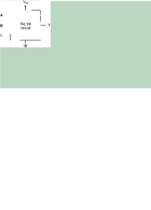
Suppose we have an unknown digital circuit, represented by the block in Figure 3.16. All we know is which terminals are inputs, which are outputs, and how to connect the power supply. Given only that information, we can find the Boolean expression of the output.
The first thing to do is find the truth table by applying all possible input combinations in binary order and reading the output for each one. Suppose the unknown circuit in Figure 3.16 yields the truth table shown in Table 3.4.
The truth table output is HIGH for three conditions:
1.When A AND B AND C are all LOW, OR
2.When A is LOW AND B AND C are HIGH, OR
3.When A is HIGH AND B AND C are LOW.
FIGURE 3.16 |
Table 3.4 |
Truth |
|
||
Digital Circuit with |
Table for Figure 3.19 |
||||
Unknown Function |
|
|
|
|
|
A |
B |
C |
|
Y |
|
|
|
||||
|
|
|
|
|
|
|
0 |
0 |
0 |
|
1 |
|
0 |
0 |
1 |
|
0 |
|
0 |
1 |
0 |
|
0 |
|
0 |
1 |
1 |
|
1 |
|
1 |
0 |
0 |
|
1 |
|
1 |
0 |
1 |
|
0 |
|
1 |
1 |
0 |
|
0 |
|
1 |
1 |
1 |
|
0 |
|
|
|
|
|
|
Each of those conditions represents a minterm in the output Boolean expression. (A minterm is a product term (AND term) that includes all variables (A, B, C) in true or complement form.) The minterms are:
1.A B C
2.A B C
3.A B C
68 C H A P T E R 3 • Boolean Algebra and Combinational Logic
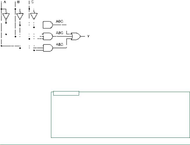
Since condition 1 OR condition 2 OR condition 3 produces a HIGH output from the circuit, the Boolean function Y consists of all three minterms summed (ORed) together, as follows:
Y A B C A B C A B C
This expression is in a standard form called sum-of-products (SOP) form. Figure 3.17 shows the equivalent logic circuit.
FIGURE 3.17
Logic Circuit for Y A B C ABC A B C
The inputs A, B, and C and their complements are shown in bus form. Each variable is available, in true or complement form, at any point along a conductor. This is a useful, uncluttered notation for circuits that require several of the input variables more than once.
N O T E
We can derive an SOP expression from a truth table as follows:
1.Every line on the truth table that has a HIGH output corresponds to a minterm in the truth table’s Boolean expression.
2.Write all truth table variables for every minterm in true or complement form. If a variable is 0, write it in complement form (with a bar over it); if it is 1, write it in true form (no bar).
3.Combine all minterms in an OR function.
EXAMPLE 3.7 |
Tables 3.5 and 3.6 show the truth tables for the Exclusive OR and the Exclusive NOR func- |
|||||||||
|
tions. Derive the sum-of-products expression for each of these functions and draw the logic |
|||||||||
|
diagram for each one. |
|
|
|
|
|
||||
|
Table 3.5 |
XOR |
Table 3.6 |
XNOR |
||||||
|
Truth Table |
|
|
Truth Table |
|
|
||||
|
|
|
|
|
|
|
|
|
|
|
|
A |
B |
|
A B |
A |
B |
|
|
|
|
|
A B |
|||||||||
|
|
|
|
|
|
|
|
|
|
|
|
0 |
0 |
|
0 |
|
0 |
0 |
|
1 |
|
|
0 |
1 |
|
1 |
|
0 |
1 |
|
0 |
|
|
1 |
0 |
|
1 |
|
1 |
0 |
|
0 |
|
|
1 |
1 |
|
0 |
|
1 |
1 |
|
1 |
|
|
|
|
|
|
|
|
|
|
|
|
3.2 • Sum-of-Products and Product-of-Sums Forms |
69 |
Solution
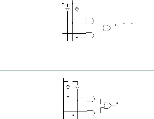
XOR: The truth table yields two product terms: AB and AB. Thus, the SOP form of the XOR function is A B AB AB. Figure 3.18 shows the logic diagram for this equation.
A B
A B AB AB
FIGURE 3.18
Example 3.7
SOP Form of XOR Function
XNOR: The product terms for this function are: A B and AB. The SOP form of the XNOR function is A B A B AB. The logic diagram in Figure 3.19 represents the XNOR
function. |
|
|
A B
A B AB AB
FIGURE 3.19
Example 3.7
SOP Form of XNOR Function
We can also find the Boolean function of a truth table in product-of-sums (POS) form. The product-of-sums form of a Boolean expression consists of a number of maxterms (i.e., sum terms (OR terms) containing all variables in true or complement form) that are ANDed together. To find the POS form of Y, we will find the SOP expression for Y and apply DeMorgan’s theorems.
Recall DeMorgan’s theorems:
x y z x y zx y z x y z
When the theorems were introduced, they were presented as two-variable theorems, but in fact they are valid for any number of variables.