

Digital design with CPLD applications and VHDL (R. Dueck, 2000)
.pdf150 C H A P T E R 4 • Introduction to PLDs and MAX+PLUS II
‘-’ — — Don’t care
25.STD_LOGIC is defined in a library called ieee. To use STD LOGIC, include the following two statements at the beginning of a file
LIBRARY ieee;
USE ieee.std_logic_1164.ALL;
26.A port in VHDL is an input or output. A signal is an internal connection, like a wire. A variable is a piece of working memory reserved by the VHDL file.
27.The simplest way to relate inputs and outputs in a VHDL design is with a concurrent signal assignment statement, which
has the form: x <= (a and b) or c; The port or signal on the left side is assigned the value of the logic expression on the right side. (Variables are assigned with a different operator.)
28.A port, signal, or variable can have a multiple-bit construction of type BIT_VECTOR or STD_LOGIC_VECTOR.
These structures are called vectors and can be referred to a separate elements (e.g., y(3) <= d(1) and d(0);) or as a group (e.g., y <= “1000”).
29.A selected signal assignment statement can act as a truth table in VHDL. It assigns alternative values to one or more outputs, depending on the alternative values on one or more inputs.
30.VHDL constructs and statements can be selected in generic form from a template menu in MAX PLUS II.
31.VHDL designs can be embedded in a gdf as default symbols.
32.Pin numbers must be assigned to a design before it can be downloaded to a CPLD. Pins can be assigned in the Pin/ Location/Chip dialog box (accessed by highlighting a pin symbol and right-clicking) or by editing the project’s Assignment and Configuration File (acf).
33.An Altera CPLD can be programmed directly from a PC parallel port via a ByteBlaster cable.
34.The ByteBlaster cable implements a programming interface specified by a standard (IEEE Std. 1149.1) of the Joint Test Action Group (JTAG).
35.A JTAG port is a 4-wire interface for loading test and programming information into one or more JTAG-compliant devices. It consists of an input (TDI), output (TDO), mode select (TMS), and clock (TCK).
Bit string literal A group of bits assigned to the elements of a vector, enclosed in double quotes (e.g., “001011”).
ByteBlaster An Altera ribbon cable and connector used to program or configure Altera CPLDs via the parallel port (LPT port) of an IBM PC or compatible.
Comment Explanatory text in a VHDL (or other computer language) file that is ignored by the computer at compile time.
Compile The process used by CPLD design software to interpret design information (such as a drawing or text file) and create required programming information for a CPLD.
Complex PLD (CPLD) A digital device consisting of several programmable sections with internal interconnections between the sections.
Concurrent Simultaneous.
Concurrent signal assignment A relationship between an input and output port or signal in which the output is changed as soon as there is a change in input. If the file has more than one concurrent signal assignment, they are all evaluated simultaneously.
Default symbol A graphical symbol that represents a PLD design as a block, showing only the design’s inputs and outputs. The symbol can be used as a component in any Graphic Design File.
Design entry The process of using software tools to describe the design requirements of a PLD. Design entry can be done by entering a schematic or a text file that describes the required digital function.
Download Program a PLD from a computer running PLD design and programming software.
Entity A VHDL structure that defines the inputs and outputs of a design.
Fitting Assigning internal PLD circuitry, as well as input and output pins, for a PLD design.
Graphic Design File (gdf) A PLD design file in which the digital design is entered as a schematic.
Hardware description language A computer language used to design digital circuits by entering text-based descriptions of the circuits.
G L O S S A R Y
AHDL (Altera Hardware Description Language) Altera’s proprietary text-entry design tool for PLDs.
Altera UP-1 Board A circuit board, part of Altera’s University Program Design Laboratory Package, containing two CPLDs and a number of input and output devices.
Architecture A VHDL structure than defines the relationship between input, output, and internal signals or variables in a design.
ASICs (application specific integrated circuits) Integrated circuits that are constructed for a specific design purpose. The term could refer to a PLD, although it usually means a customdesigned fixed function device.
Assignment and Configuration File (acf) A MAX PLUS II file that contains information about the configuration options for a project, including assigned device and pin numbers.
Hierarchical design A PLD design that is ordered in layers or levels. The highest level of design contains components that are themselves complete designs. These components may, in turn, have lower-level designs embedded within them.
ICR In-circuit reconfigurability. The ability of a PLD (such as a FLEX10K) to be configured without removing it from a circuit board.
IEEE Standard 1164 The standard which defines a variety of VHDL types and operations, including the STD_LOGIC and STD_LOGIC_VECTOR types.
ISP In-system programmability. The ability of a PLD (such as a MAX7000S) to be programmed without removing it from a circuit board.
JTAG Joint Test Action Group. A standards body that developed the format (called IEEE Std. 1149.1) for testing and programming devices while they are installed in a system.

Problems 151
JTAG Chain Multiple JTAG-compliant devices whose TDI and TDO ports form a continuous chain connection. Such a chain allows multi-device programming.
Library A collection of VHDL design units that have been previously compiled.
MAX PLUS II CPLD design and programming software owned by Altera Corporation.
Mode (of a port) The kind of port, such as input or output.
Nonvolatile Able to retain stored information after power is removed.
Package A group of VHDL design elements that can be used by more than one VHDL file.
Port A name assigned to an input or output of a VHDL design entity.
Programmable logic device (PLD) A digital integrated circuit that can be programmed by the user to implement any digital logic function.
Programmer Object File (pof) Binary file used to program a PLD of the Altera MAX series.
Programming Transferring design information from the computer running PLD design software to the actual PLD chip.
Project A set of MAX PLUS II files associated with a particular PLD design.
Schematic capture A technique of entering CPLD design information by using a CAD (computer aided design) tool to draw a logic circuit as a schematic. The schematic can then be interpreted by design software to generate programming information for the CPLD.
Selected signal assignment statement A concurrent signal assignment in VHDL in which a value is assigned to a signal, depending on the alternative values of another signal or variable.
Signal A name given to an internal connection in a VHDL architecture.
Simulation Verifying design function by specifying a set of inputs and observing the resultant outputs. Simulation is generally shown as a series of input and output waveforms.
S0
S1
D0
D1
Y
D2
D3
FIGURE 4.48
Problem 4.4
4-to-1 Multiplexer
Software tools Specialized computer programs used to perform specific functions such as design entry, compiling, fitting, and so on. (Sometimes just called “tools”.)
SRAM Object File (sof) Binary file used to configure a PLD of the Altera FLEX series.
Suite (of software tools) A related collection of tools for performing specific tasks. MAX PLUS II is a suite of tools for de-
signing and programming digital functions in a PLD.
Syntax The “grammar” of a computer language (i.e., the rules of construction of language statements).
Target device The specific PLD for which a digital design is intended.
TCK Test Clock. The JTAG signal that drives the JTAG downloading process from one state to the next.
Table 4.3 Pin Assignments for
Multiplexer Circuit
Function |
Pin |
|
|
S1 |
12 |
S0 |
16 |
D0 |
15 |
D1 |
17 |
D2 |
21 |
D3 |
25 |
Y |
4 |
|
|
TDI Test Data In. In a JTAG port, the serial input data to a device.
TDO Test Data Out. The JTAG signal, the serial output data from a device.
S0 |
|
S1 |
|
D |
Y0 |
|
|
|
Y1 |
|
Y2 |
|
Y3 |
FIGURE 4.49
Problem 4.9
4-channel Demultiplexer
152 C H A P T E R 4 • Introduction to PLDs and MAX+PLUS II
TMS Test Mode Select. The JTAG signal that controls the downloading of test or programming data.
Top level (of a hierarchy) The file in a hierarchy that contains components specified in other design files and is not itself a component of a higher-level file.
Table 4.4 Pin Assignments for Demultiplexer Circuit
Function |
Pin |
|
|
S1 |
12 |
S0 |
16 |
D |
15 |
Y0 |
4 |
Y1 |
6 |
Y2 |
8 |
Y3 |
10 |
|
|
Table 4.5 Pin Assignments for Equality Comparator
Function |
Pin |
|
|
A1 |
12 |
A2 |
16 |
B1 |
15 |
B2 |
17 |
AEQB |
4 |
|
|
a gdf file.
Variable A block of working memory used for internal calculation or storage in a VHDL architecture.
Vector A group of digital signals or variables, usually related numerically, that can be treated as a single multi-bit variable.
VHDL (VHSIC Hardware Description Language) An in-
Type A set of characteristics associated with a VHDL port name, signal, or variable that determines the allowable values of the port, signal, or variable.
User library A folder containing symbols that can be used in
A
SUM
B
CARRY
|
|
|
|
|
|
|
|
|
|
FIGURE 4.51 |
||||
A1 |
|
|
|
|
|
|
|
|
|
Problem 4.11 |
||||
|
|
|
Half Adder |
|||||||||||
B1 |
|
|
|
|
|
|
|
|
|
|||||
|
|
|
|
|
|
|
|
|
AEQB |
|||||
A2 |
|
|
|
|
|
|
|
|
|
|||||
|
|
|
|
|
|
|
|
|
|
|
|
|||
B2 |
|
|
|
|
|
|
|
|
dustry-standard computer language used to model digital circuits |
|||||
|
|
|
|
|||||||||||
|
|
|
|
|
|
|
|
|
|
|||||
FIGURE 4.50 |
|
and produce programming data for PLDs. |
||||||||||||
Problem 4.10 |
|
VHSIC Very high speed integrated circuit |
||||||||||||
2-bit Equality Comparator |
|
Volatile A device is volatile if it does not retain its stored in- |
||||||||||||
|
|
|
|
|
|
|
|
|
|
|||||
|
|
|
|
|
|
|
|
A |
|
|
|
|
|
|
|
|
|
|
|
|
|
|
B |
|
|
|
|
|
SUM |
|
|
|
|
|
|
|
|
|
|
|
|
|
||
|
|
|
|
|
|
|
|
|
|
|
|
|
||
|
|
|
|
|
|
|
|
|
|
|
|
|
|
|
CARRY
IN CARRY OUT
FIGURE 4.52
Problem 4.12
Full Adder
formation after the power to the device is removed.
P R O B L E M S
Table 4.6 Pin Assignments for
Full Adder
Function Pin
A12
B15
CARRY IN |
33 |
SUM |
6 |
CARRY OUT |
4 |
Section 4.1 What Is a PLD?
4.1List some of the advantages of programmable logic over fixed-function logic.
4.2What does CPLD stand for? How is it different from the term PLD?
4.3List some types of PLDs other than CPLDs.
4.4Figure 4.48 shows a 4-to-1 multiplexer circuit. (The circuit switches one of four digital inputs to a single output, depending on the states of two “select inputs.”) State the number of 74HC type devices required to make this circuit. You may use the following devices: 74HC04 hex inverter; 74HC11 triple 3-input AND gate; 74HC4002 dual 4-input NOR gate (there are no 4-input OR devices available in the 74HC family). State how many devices are required to make two multiplexers.
Section 4.3 Graphic Design File
Section 4.4 Compiling MAX PLUS II Files
4.5Briefly describe the difference between a design file and a project in MAX PLUS II.
4.6State two ways to set the MAX PLUS II project to the current file.
4.7State the definitions of the following terms:
Problems 153
a.primitives
b.instance
4.8Use MAX PLUS II to create a Graphic Design File for the multiplexer circuit shown in Figure 4.48. Save the file as drive:\max2work\chapt4\problems\4to1mux.gdf. Assign pins as in Table 4.3. Set the project to the current file and compile.
4.9Figure 4.49 shows the circuit for a 4-channel demultiplexer, which switches a digital input to one of four outputs, depending in the states of two “select inputs.” Figure 4.49
Use MAX PLUS II to create a Graphic Design File for the demultiplexer circuit. Save the file as drive:\max2work\chapt4\problems\4ch_dmux.gdf. Assign pins as in Table 4.4. Set the project to the current file and compile.
4.10Repeat Problem 4.9 for the 2-bit equality comparator in Figure 4.50. This circuit generates a HIGH output when
the two 2-bit numbers A2A1 and B2B1 are equal. Save the file as drive:\max2work\chapt4\problems\eq_comp. gdf. Use the pin assignments in Table 4.5.
4.11Use MAX PLUS II to create a Graphic Design File for the half-adder circuit shown in Figure 4.51. The halfadder adds 2 bits to generate a sum and a carry output. Save the file as drive:\max2work\chapt4\problems\ halfadd.gdf. Create a default symbol for the file and compile, after setting the project to the current file. Do not assign pin numbers at this time.
4.12Use MAX PLUS II to create a Graphic Design File for the full adder circuit shown in Figure 4.52. The full adder combines two bits A and B, plus an input carry from a previous stage to generate a sum and a carry output.
Save the file as drive:\max2work\chapt4\problems\fulladd.gdf. Assign pin numbers as shown in Table 4.6. Set the project to the current file and compile.
4.13Examine the half adder circuit in Figure 4.51 and the full adder circuit in Figure 4.52. You should find two half adders in the full adder circuit. Use the half adder symbol you created in Problem 4.11 to create a full adder as a hierarchical design, consisting of two half adders and other logic. Save the file as drive:\max2work\chapt4\
C H A P T E R 5
Combinational Logic Functions
O U T L I N E
5.1Decoders
5.2Encoders
5.3Multiplexers
5.4Demultiplexers
5.5Magnitude Comparators
5.6Parity Generators and Checkers
C H A P T E R O B J E C T I V E S
Upon successful completion of this chapter you will be able to:
•Design binary decoders using logic gates.
•Create decoder designs in MAX PLUS II, using Graphic Design Files or VHDL.
•Create MAX PLUS II simulation files to verify the operation of combinational circuits.
•Design BCD-to-seven-segment and hexadecimal-to-seven-segment decoders, including special features such as ripple blanking, using VHDL and Graphic Design Files in MAX PLUS II.
•Use MAX PLUS II Graphic Design Files and VHDL to generate the design for a 3-bit binary and a BCD priority encoder.
•Describe the circuit and operation of a simple multiplexer and program these functions in VHDL.
•Draw logic circuits for multiplexer applications, such as single-channel data selection, multibit data selection, waveform generation, and timedivision multiplexing (TDM).
•Describe demultiplexer circuits and program them using VHDL.
•Define the operation of a CMOS analog switch and its use in multiplexers and demultiplexers.
•Define the operation of a magnitude comparator and program its function in VHDL.
•Explain the use of parity as an error-checking system and draw simple parity-generation and checking circuits..
Anumber of standard combinational logic functions have been developed for digital circuits that represent many of the useful tasks that can be performed with digital
circuits.
Decoders detect the presence of particular binary states and can activate other circuits based on their input values or can convert an input code to a different output code. Encoders generate a binary or binary coded decimal (BCD) code corresponding to an active input.
Multiplexers and demultiplexers are used for data routing. They select a transmission path for incoming or outgoing data, based on a selection made by a set of binary-related inputs.
155

156 C H A P T E R 5 • Combinational Logic Functions
Magnitude comparators determine whether one binary number is less than, greater than, or equal to another binary number.
Parity generators and checkers are used to implement a system of checking for errors in groups of data.
5.1 Decoders
K E Y T E R M S
Decoder A digital circuit designed to detect the presence of a particular digital
state.
The general function of a decoder is to activate one or more circuit outputs upon detection of a particular digital state. The simplest decoder is a single logic gate, such as a NAND or AND, whose output activates when all its inputs are HIGH. When combined with one or more inverters, a NAND or AND can detect any unique combination of binary input values.
An extension of this type of decoder is a device containing several such gates, each of which responds to a different input state. Usually, for an n-bit input, there are 2n logic gates, each of which decodes a different combination of input variables. A variation is a BCD device with 4 input variables and 10 outputs, each of which activates for a different BCD input.
Some types of decoders translate binary inputs to other forms, such as the decoders that drive seven-segment numerical displays, those familiar figure-8 arrangements of LED or LCD outputs (“segments”). The decoder has one output for every segment in the display. These segments illuminate in unique combinations for each input code.
Single-Gate Decoders
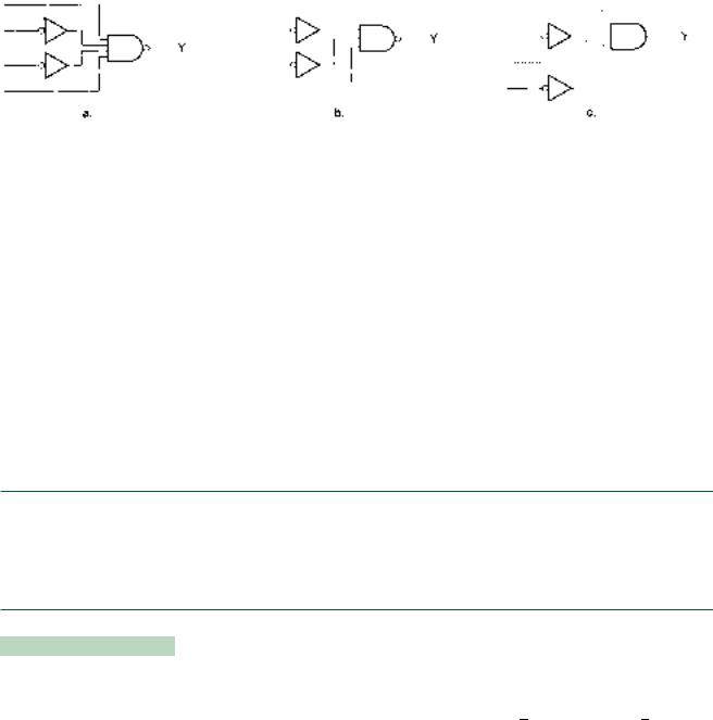
The simplest decoder is a single gate, sometimes in combination with one or more inverters, used to detect the presence of one particular binary value. Figure 5.1 shows two such decoders, both of which detect an input D3D2D1D0 1111.
D3 |
|
|
|
D2 |
|
|
|
Y D3D2D1D0 |
|||
D1 |
|||
|
|
||
D0 |
|
|
|
FIGURE 5.1
Single-Gate Decoders
The decoder in Figure 5.1a generates a logic HIGH when its input is 1111. The decoder in Figure 5.1b responds to the same input, but makes the output LOW instead.
In Figure 5.1, we designate D3 as the most significant bit of the input and D0 the least
|
significant bit. We will continue this convention for multi-bit inputs. |
|
In Boolean expressions, we will indicate the active levels of inputs and outputs sepa- |
|
rately. For example, in Figure 5.1, the inputs to both gates are the same, so we write |
|
D3D2D1D0 for the inputs of both gates. The gates in Figures 5.1a and b have outputs with |
|
opposite active levels, so we write the output variables as complements (Y and Y ). |
|
|
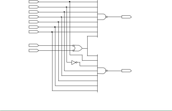
EXAMPLE 5.1 |
Figure 5.2 shows three single-gate decoders. For each one, state the output active level and |
|
the input code that activates the decoder. Also write the Boolean expression of each output. |
5.1 • Decoders |
157 |
D3
D2
D1
D0
FIGURE 5.2
Example 5.1
Single-Gate Decoders
Solution Each decoder is a NAND or AND gate. For each of these gates, the output is active when all inputs are HIGH. Because of the inverters, each circuit has a different code that fulfils this requirement.
Figure 5.2a: Output: Active LOW
Input code: D3D2D1D0 1001
Y D3D2D1D0
Figure 5.2b: Output: Active LOW
Input code: D2D1D0 001
Y D2D1D0 |
|
Figure 5.2c: Output: Active HIGH |
|
Input code: D3D2D1D0 1010 |
|
Y D3D2D1D0 |
|
|
Single-gate decoders are often used to activate other digital circuits under various operating conditions, particularly if there is a choice of circuits to activate. For example, single-gate decoders are used to enable peripheral devices in a personal computer (PC). A combination of binary values, called the address, specifies a unique set of conditions to enable a particular peripheral device.
EXAMPLE 5.2
Application
A PC has two serial port cards called COM1 and COM2. Each card is activated when either one of two control inputs called IOR (Input/Output Read) and IOW (Input/Output Write) are active and a unique 10-bit address is present. IOR and IOW are active-LOW. The address is specified by bits A9 A8 A7 A6 A5 A4 A3 A2 A1 A0, which can be represented by three hexadecimal digits. The decoder outputs, COM1 Enable and COM2 Enable are both active-LOW.
The card for COM1 activates when (IOR OR IOW is LOW) AND the address is between 3F8H and 3FFH.
The card for COM2 activates when (IOR OR IOW is LOW) AND the address is between 2F8H and 2FFH.
Create a Graphic Design File in MAX PLUS II that implements the specified decoder.
Solution The lowest address that activates COM1 is
A9 A8 A7 A6 A5 A4 A3 A2 A1 A0 3F8H 11 1111 1000
The highest COM1 address is
A9 A8 A7 A6 A5 A4 A3 A2 A1 A0 3FFH 11 1111 1111
158 C H A P T E R 5 • Combinational Logic Functions
A9
A8
A7
A6
A5
A4
A3
IOW
IOR
Since any address in this range is valid, we can represent the last three bits, A2 A1A0, as don’t care states. Thus, for COM1, we should decode the address:
A9 A8 A7 A6 A5 A4 A3 A2 A1 A0 11 1111 1XXX
Similarly, for COM2:
Low address: A9 A8 A7 A6 A5 A4 A3 A2 A1 A0 2F8H 10 1111 1000 High address: A9 A8 A7 A6 A5 A4 A3 A2 A1 A0 2FFH 10 1111 1111 Decode: A9 A8 A7 A6 A5 A4 A3 A2 A1 A0 10 1111 1XXX
Figure 5.3 shows the gdf representation of the decoder circuit, including inputs for the control signals IOR and IOW.
NAND8
INPUT
INPUT
INPUT
INPUT
INPUT
INPUT
INPUT
INPUT |
BOR2 |
INPUT |
|
NAND8 |
NOT |
OUTPUT
COM1_Enable
OUTPUT
COM2_enable
FIGURE 5.3
Example 5.2
COM Port Decoders
SECTION 5.1A REVIEW PROBLEM
5.1Draw a single-gate decoder that detects the input state D3D2D1D0 1100
a.with active-HIGH indication
b.with active-LOW indication
Multiple-Output Decoders
Decoder circuits often are constructed with multiple outputs. In effect, such a device is a collection of decoding gates controlled by the same inputs. A decoder circuit with n inputs can activate up to m 2n load circuits. Such a decoder is usually described an n-line-to-m- line decoder.
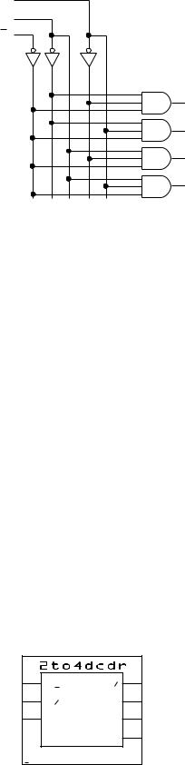
5.1 • Decoders |
159 |
D0
D1
G
Y0
Y1
Y2
Y3
FIGURE 5.4
2-line-to-4-line Decoder with Enable
Figure 5.4 shows the logic circuit of a 2-line-to-4-line decoder. The circuit detects the presence of a particular state of the 2-bit input D1D0, as shown by the truth table in Table 5.1. One and only one output is HIGH for any input combination, provided the enable input G is LOW. The active input of each line is shown in boldface. The subscript of the active output is the same as the value of the 2-bit input. For example, if D1D0 10, output Y2 is active since 10 (binary) 2 (decimal).
Table 5.1 Truth Table of a 2-to-4 Decoder with Enable
G |
D1 |
D0 |
Y0 |
Y1 |
Y2 |
Y3 |
|
|
|
|
|
|
|
0 |
0 |
0 |
1 |
0 |
0 |
0 |
0 |
0 |
1 |
0 |
1 |
0 |
0 |
0 |
1 |
0 |
0 |
0 |
1 |
0 |
0 |
1 |
1 |
0 |
0 |
0 |
1 |
1 |
X |
X |
0 |
0 |
0 |
0 |
|
|
|
|
|
|
|
If we are using the decoder to activate one of four output loads, it is possible that there are situations where we want no output to be active. In such a case, we can deactivate all outputs (make them all LOW) by setting G HIGH.
We can create the 2-line-to-4-line decoder of Figure 5.4 as a graphic or text file in MAX PLUS II and create a symbol for it that can be used in higher-level graphic files. Figure 5.5 shows the symbol for the decoder.
FIGURE 5.5
MAX PLUS II Graphic Symbol for a 2-to-4 Decoder with Enable
D1 |
Y0 |
D0 |
Y1 |
G |
Y2 |
|
Y3 |
1 |
|