

Digital design with CPLD applications and VHDL (R. Dueck, 2000)
.pdf170 C H A P T E R 5 • Combinational Logic Functions
decode4g.vhd
PORT( |
|
|
d |
: IN |
INTEGER RANGE 0 to 3; |
g |
: IN |
STD_LOGIC; |
y |
: OUT |
STD_LOGIC_VECTOR (0 to 3)); |
END decode4g;
ARCHITECTURE a OF decode4g IS
BEGIN
y <=
END a;
MAX PLUS II Report File
In the Altera Golden Rules, we are told to choose a selected signal assignment over a conditional signal assignment because it uses the CPLD resources more efficiently. How do we check this assertion? Is it always true? This information is stored in a MAX PLUS II report file (rpt), which is created at compile time.
The compile process of MAX PLUS II goes on behind the scenes; until now we have not enquired about the result of this process. One of many functions of the compiler is to reduce the design information in a graphic or text file to a series of Boolean equations that can be programmed into a PLD.
For example, the report file decode3a.rpt, for the file that uses the selected signal assignment, gives us the following information under the EQUATIONS heading.
|
|
** EQUATIONS ** |
|
|
||
|
d0 |
: INPUT; |
|
|
||
|
decode3a.rpt |
|
|
|||
|
|
d1 |
: INPUT; |
|
|
|
|
|
g |
: INPUT; |
|
|
|
|
|
—— Node name is ‘y0’ |
|
|||
|
|
—— Equation name is ‘y0’, location is LC117, type is output. |
||||
|
|
y0 |
= |
LCELL( _EQ001 $ |
GND); |
|
|
|
_EQ001 = |
!d0 & !d1 & !g; |
|
||
|
|
—— Node name is ‘y1’ |
|
|||
|
|
—— Equation name is ‘y1’, location is LC115, type is output. |
||||
|
|
y1 |
= |
LCELL( _EQ002 $ |
GND); |
|
|
|
_EQ002 = |
d0 & !d1 & !g; |
|
||
|
|
—— Node name is ‘y2’ |
|
|||
|
|
—— Equation name is ‘y2’, location is LC118, type is output. |
||||
|
|
y2 |
= |
LCELL( |
_EQ003 $ |
GND); |
|
|
_EQ003 = !d0 & |
d1 & !g; |
|
||
|
|
—— Node name is ‘y3’ |
|
|||
|
|
—— Equation name is ‘y3’, location is LC120, type is output. |
||||
|
|
y3 |
= |
LCELL( |
_EQ004 $ |
GND); |
|
|
_EQ004 = |
d0 & |
d1 & !g; |
|
|
Each output is designated as a node. Let us examine the equation of one node in detail so that we will know how to interpret the others.

5.1 • Decoders |
171 |
The Boolean format in the report file uses different operators than VHDL. They are as follows:
! = NOT
& = AND
# = OR
$ = XOR
Thus, the equation given as _EQ001 = !d0 & !d1 & !g is equivalent to the Boolean expression _EQ001 d0 d1 g.
In the expression (y0 = LCELL ( _EQ001 $ GND);), equation _EQ001 is XORed with GND (logic 0) and applied to an LCELL (logic cell) primitive to yield y0. The LCELL represents one output of the CPLD. The XOR function is a way to either invert or not invert a logic function by setting one XOR input to GND (noninverting) or VCC (inverting). Thus _EQ001 is applied to a CPLD output without inversion.
A comment in the report file indicates that y0 is assigned to logic cell LC117 (out of 128), which corresponds to pin 75 (out of 84) on the CPLD. Other equations are assigned to other LCELLs with other Boolean functions, as appropriate. Every pin number on the CPLD package is permanently connected to a specific LCELL. The compiler chooses the LCELL/pin assignments automatically; if we desire specific pin number assignments, we must assign them explicitly before compiling.
decode4g.rpt
decoder with enable, the two statement forms are easy enough for the compiler to interpret both in the most efficient way.
|
a |
||
f |
|
b |
|
g |
|||
|
|
||
e |
|
c |
|
|
|
|
|
d
FIGURE 5.22
Seven-segment Numerical
Display
Seven-Segment Decoders
K E Y T E R M S
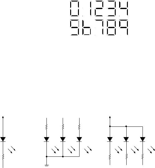
Seven-segment display An array of seven independently controlled light-emit- ting diode (LED) or liquid crystal display (LCD) elements, shaped like a figure-8, which can be used to display decimal digits and other characters by turning on the appropriate elements.
Common anode display A seven-segment LED display where the anodes of all
the LEDs are connected to the circuit supply voltage. Each segment is illuminated by a logic LOW at its cathode.
Common cathode display A seven-segment display in which the cathodes of all LEDs are connected together and grounded. A logic HIGH illuminates a segment when applied to its anode.
Display
The seven-segment display, shown in Figure 5.22, is a numerical display device used to show digital circuit outputs as decimal digits (and sometimes hexadecimal digits or other alphabetic characters). It is called a seven-segment display because it consists of seven luminous segments, usually LEDs or liquid crystals, arranged in a figure-8. We can display any decimal digit by turning on the appropriate elements, designated by lowercase letters, a through g. It is conventional to designate the top segment as a and progress clockwise around the display, ending with g as the center element.
Figure 5.23 shows the usual convention for decimal digit display. Some variation from this convention is possible. For example, we could have drawn the digits 6 and 9 with “tails” (i.e., with segment a illuminated for 6 or segment d for 9). By convention, we
172 C H A P T E R 5 • Combinational Logic Functions
FIGURE 5.23
Convention for Displaying Decimal Digits
display digit 1 by illuminating segments b and c, although segments e and f would also work.
The electrical requirements for an LED circuit are simple. Since an LED is a diode, it conducts when its anode is positive with respect to its cathode, as shown in Figure 5.24a. A decoder/driver for an LED display will illuminate an element by completing this circuit, either by supplying VCC or ground. A series resistor limits the current to prevent the diode from burning out and to regulate its brightness. If the anode is 5 volts with respect to cathode, the resistor value should be in the range of 220 to 470 .
Vcc |
a |
b |
c |
Vcc |
|
|
|
|
|
|
|
|
a |
b |
c |
|
|
|
|
|
|
|
||||
|
|
|
|
|
|
|
||||
|
|
|
|
|
|
|
||||
a. Circuit requirements for |
|
b. Common cathode |
b. Common anode |
|||||||
an illuminated LED |
|
|
|
|
||||||
FIGURE 5.24
Electrical Requirements for LED Displays
Seven-segment displays are configured as common anode or common cathode, as shown in Figures 5.24b and c. In a common cathode display, the cathodes of all LEDs are connected together and brought out to one or more pin connections on the display package. The cathode pins are wired externally to the circuit ground. We illuminate the segments by applying logic HIGHs to individual anodes.
Similarly, the common anode display has the anodes of the segments brought out to one or more common pins. These pins must be tied to the circuit power supply (VCC). The segments illuminate when a decoder/driver makes their individual cathodes LOW. Figure 5.25 shows how the diodes could be physically laid out in a common anode display.
The two types of displays allow the use of either active HIGH or active LOW circuits to drive the LEDs, thus giving the designer some flexibility. However, it should be noted that the majority of seven-segment decoders are for common-anode displays.
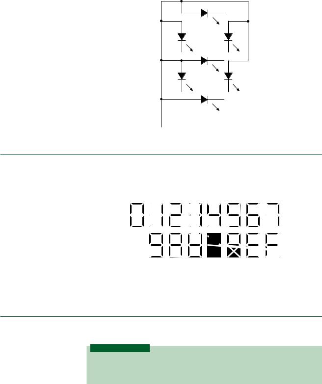
FIGURE 5.25
Physical Placement of LEDs in a
Common Anode Display
5.1 • Decoders |
173 |
|
a |
f |
b |
|
g |
e |
c |
|
d |
Vcc
EXAMPLE 5.4 |
Sketch the segment patterns required |
|
segment display. What changes from |
display all 16 hexadecimal digits on a sevenpatterns in Figure 5.23 need to be made?
Solution The segment patterns are |
in Figure 5.26. |
||
|
|
|
|
|
|
|
|
Hex digits B and D must be displayed as lowercase letters, b and d, to avoid confusion between B and 8 and between D and 0. To make 6 distinct from b, 6 must be given a tail
(segment a) and to make 6 and 9 symmetrical, 9 should also have a tail (segment d ). |
|
|
Decoder
K E Y T E R M S
BCD Binary coded decimal. A code in which each individual digit of a decimal number is represented by a 4-bit binary number (e.g., 905 (decimal) 1001 0000 0101 (BCD)).
A BCD-to-seven-segment decoder is a circuit with a 4-bit input for a BCD digit and seven outputs for segment selection. To display a number, the decoder must translate the input bits to a combination of active outputs. For example, the input digit D3D2D1D0 0000 must illuminate segments a, b, c, d, e, and f to display the digit 0. We can make a truth

174 C H A P T E R 5 • Combinational Logic Functions
table for each of the outputs, showing which must be active for every digit we wish to display. The truth table for a common-anode decoder (active LOW outputs) is given in Table 5.3.
Table 5.3 Truth Table for Common Anode BCD-to-Seven-Segment Decoder
Digit |
D3 |
D2 |
D1 |
D0 |
a |
b |
c |
d |
e |
f |
g |
|
|
|
|
|
|
|
|
|
|
|
|
0 |
0 |
0 |
0 |
0 |
0 |
0 |
0 |
0 |
0 |
0 |
1 |
1 |
0 |
0 |
0 |
1 |
1 |
0 |
0 |
1 |
1 |
1 |
1 |
2 |
0 |
0 |
1 |
0 |
0 |
0 |
1 |
0 |
0 |
1 |
0 |
3 |
0 |
0 |
1 |
1 |
0 |
0 |
0 |
0 |
1 |
1 |
0 |
4 |
0 |
1 |
0 |
0 |
1 |
0 |
0 |
1 |
1 |
0 |
0 |
5 |
0 |
1 |
0 |
1 |
0 |
1 |
0 |
0 |
1 |
0 |
0 |
6 |
0 |
1 |
1 |
0 |
1 |
1 |
0 |
0 |
0 |
0 |
0 |
7 |
0 |
1 |
1 |
1 |
0 |
0 |
0 |
1 |
1 |
1 |
1 |
8 |
1 |
0 |
0 |
0 |
0 |
0 |
0 |
0 |
0 |
0 |
0 |
9 |
1 |
0 |
0 |
1 |
0 |
0 |
0 |
1 |
1 |
0 |
0 |
|
|
|
|
|
|
||||||
|
1 |
0 |
1 |
0 |
X X X X X X X |
||||||
|
1 |
0 |
1 |
1 |
X X X X X X X |
||||||
Invalid Range |
1 |
1 |
0 |
0 |
X |
X |
X |
X |
X |
X |
X |
|
1 |
1 |
0 |
1 |
X X X X X X X |
||||||
|
1 |
1 |
1 |
0 |
X X X X X X X |
||||||
|
1 |
1 |
1 |
1 |
X X X X X X X |
||||||
|
|
|
|
|
|
|
|
|
|
|
|
The illumination of each segment is determined by a Boolean function of the input variables, D3D2D1D0. From the truth table, the function for segment a is
a D3D2D1D0 D3D2D1D0 D3D2D1D0
(Since the display is active-LOW, this means segment a is OFF for digits 1, 4, and 6.)
If we assume that inputs 1010 to 1111 are never going to be used (“don’t care states”, symbolized by X), we can make any of these states produce HIGH or LOW outputs, depending on which is most convenient for simplifying the segment functions. Figure 5.27a shows a Karnaugh map simplification for segment a. The resultant function is
a D3D2D1D0 D2D0
The corresponding partial decoder is shown in Figure 5.27b.
We could do a similar analysis for each of the other segments, but if we are programming the decoder function into a CPLD, it is just as simple to write the truth table directly into a selected signal assignment statement, as shown in the VHDL code that follows.
——bcd_7seg.vhd
——BCD-to-seven-segment decoder
ENTITY bcd_7seg IS |
|
|
|
PORT( |
|
|
|
d3, d2, d1, |
d0 |
: IN |
BIT; |
a, b, c, d, |
e, f, g |
: OUT |
BIT); |
bcd_7seg.vhd
SIGNAL input : BIT_VECTOR (3 downto 0); SIGNAL output: BIT_VECTOR (6 DOWNTO 0); BEGIN
input <= d3 & d2 & d1 & d0; WITH input SELECT
output <= “0000001” WHEN “0000”, “1001111” WHEN “0001”,
FIGURE 5.27
Decoding Segment a
5.1 • Decoders |
175 |
“0010010” WHEN “0010”, “0000110” WHEN “0011”,
“1001100” WHEN “0100”, “0100100” WHEN “0101”, “1100000” WHEN “0110”, “0001111” WHEN “0111”,
“0000000” WHEN “1000”, “0001100” WHEN “1001”, “1111111” WHEN others;
—— Separate the output vector to make individual pin outputs.
a<= output(6);
b<= output(5);
c<= output(4);
d<= output(3);
e<= output(2);
f<= output(1);
g<= output(0);
END seven_segment;
|
|
D1D0 |
|
|
|
|
|
|
|
|
|
|
|
|
|
|
|
D3D2 |
00 |
01 |
11 |
|
10 |
|
|
|
|
|
|
|
|
||||
00 |
|
0 |
1 |
0 |
|
0 |
|
|
|
|
|
|
|
|
|||
01 |
|
1 |
0 |
0 |
|
1 |
|
|
|
|
|
|
|
|
|||
11 |
|
X |
X |
X |
|
X |
|||||||||||
10 |
|
0 |
0 |
X |
|
X |
|||||||||||
|
|
|
|
|
Segment a |
|
|
|
|
|
|
|
|
|
|
||
|
|
|
|
|
a. K map |
|
|
|
|
|
|
|
|
|
|
||
D3 |
|
|
|
|
|
|
|
|
|
|
|
|
|
|
|
|
|
|
|
|
|
|
|
|
|
|
|
|
|
|
|
|
|
||
D2 |
|
|
|
|
|
|
|
|
|
|
|
|
|
|
|
|
|
|
|
|
|
|
|
|
|
|
|
|
|
|
|
|
|
|
|
D1 |
|
|
|
|
|
|
|
|
|
|
|
|
|
|
|
a |
|
|
|
|
|
|
|
|
|
|
|
|
|
|
|
|
|||
|
|
|
|
|
|
|
|
|
|
|
|
|
|
|
|||
D0 |
|
|
|
|
|
|
|
|
|
|
|
|
|
|
|
|
|
|
|
|
|
|
|
|
|
|
|
|
|
|
|
|
|
|
|
|
|
|
|
|
|
|
|
|
|
|
|
|
|
|
|
|
|
|
|
|
|
|
|
|
|
|
|
|
|
|
|
|
|
|
|
b. Decoder for segment a (common anode)
The inputs D3D2D1D0 are defined separately, then concatenated (linked in sequence) by the & operator to make a BIT_VECTOR called input. This is equivalent to the following four concurrent signal assignments:
input (3) <= d3; input (2) <= d2; input (1) <= d1; input (0) <= d0;

176 C H A P T E R 5 • Combinational Logic Functions
Why not simply define d as a vector? If we wish to create a graphic symbol for the seven-segment decoder, the above method creates a symbol shown with four separate inputs, rather than a single thick line for a 4-bit bus input. The design will work either way.
For each value of input, a signal assignment defines the output vector, each bit of which represents the value of one segment. For example, the first clause (“0000001” WHEN “0000”) sets all segments ON except segment g, thus displaying the digit “0”.
As a variation, we could define a signal called d_inputs of type INTEGER with RANGE 0 to 9. The WHEN clauses would evaluate the integer values 0 to 9, as follows.
WITH d_inputs SELECT
output <= “0000001” WHEN 0, “1001111” WHEN 1, “0010010” WHEN 2, “0000110” WHEN 3,
“1001100” WHEN 4, “0100100” WHEN 5, “0100000” WHEN 6, “0001111” WHEN 7,
“0000000” WHEN 8,
“0000100” WHEN 9,
“1111111” WHEN others; —— blank
Ripple Blanking
K E Y T E R M S
Ripple blanking A technique used in a multiple-digit numerical display that suppresses leading or trailing zeros in the display, but allows internal zeros to be displayed.
RBI Ripple blanking input
RBO Ripple blanking output
PROCESS A VHDL construct that contains statements that are executed if there is a change in a signal in its sensitivity list.
Sensitivity list A list of signals in a PROCESS statement that are monitored to determine whether the PROCESS should be executed.
CASE statement A VHDL construct in which there is a choice of statements to be executed, depending on the value of a signal or variable.
IF statement A VHDL construct within a process that executes a series of statements, if a Boolean test condition is true.
A feature often included in seven-segment decoders is ripple blanking. The ripple blanking feature allows for suppression of leading or trailing zeros in a multiple digit display, while allowing zeros to be displayed in the middle of a number.
Each display decoder has a ripple blanking input (RBI) and a ripple blanking output (RBO), which are connected in cascade, as shown in Figure 5.28. If the decoder input D3D2D1D0 is 0000, it displays digit 0 if RBI 1 and shows a blank if RBI 0.
If RBI 1 OR D3D2D1D0 is (NOT 0000), then RBO 1. When we cascade two or more displays, these conditions suppress leading or trailing zeros (but not both) and still display internal zeros.
To suppress leading zeros in a display, ground the RBI of the most significant digit decoder and connect the RBO of each decoder to the RBI of the next least significant digit. Any zeros preceding the first nonzero digit (9 in this case) will be blanked, as RBI 0 AND D3D2D1D0 0000 for each of these decoders. The 0 inside the number 904 is displayed since its RBI 1.

|
5.1 • Decoders |
177 |
|
|
|
|
|
|
FIGURE 5.28
Zero Suppression in Seven-segment Displays
Trailing zeros are suppressed by reversing the order of RBI and RBO from the above example. RBI is grounded for the least significant digit and the RBO for each decodercascades to the RBI of the next most significant digit.
We can implement the ripple blanking feature in a VHDL file by modifying the file for a standard BCDor hexadecimal-to-seven-segment decoder to include a CASE statement within a PROCESS. A PROCESS is a construct containing statements that are executed if a signal in the sensitivity list of the PROCESS changes. The general form of a PROCESS is:
PROCESS (sensitivity list)
BEGIN
statements;
END PROCESS;
A CASE statement can be one of the constructs used inside a process if we want to select among several alternatives. It takes the following form:

178C H A P T E R 5 • Combinational Logic Functions
——CASE statement within a PROCESS
PROCESS (__signal_name, __signal_name, __signal_name)
BEGIN
CASE __expression IS
WHEN __constant_value => __statement; __statement;
WHEN __constant_value => __statement; __statement;
WHEN OTHERS => __statement; __statement;
END CASE;
END PROCESS;
Whether the digit “0” is displayed or suppressed is conditional upon the value of RBI. This can be tested by an IF statement within the PROCESS. An IF statement executes one or more VHDL statements, depending on the state of a test condition. It has the following syntax.
IF __expression THEN __statement; __statement;
ELSIF __expression THEN
__statement; __statement;
ELSE
__statement; __statement;
END IF;
The following VHDL code demonstrates the ripple blanking function.
–– sevsegrb.vhd
sevsegrb.vhd |
|
nRBI, d3, d2, d1, d0 |
: IN BIT; |
a, b, c, d, e, f, g, nRBO : OUT BIT); END sevsegrb;
ARCHITECTURE seven_segment OF sevsegrb IS
SIGNAL input: BIT_VECTOR (3 DOWNTO 0);
SIGNAL output: BIT_VECTOR (6 DOWNTO 0);
BEGIN
input <= d3 & d2 & d1 & d0; —— Process Statement PROCESS (input, nRBI)
BEGIN
IF (input = “0000” and nRBI =‘0’) THEN
— — 0 suppressed
output |
<= |
“1111111”; |
nRBO |
<= |
‘0’; |
ELSIF (input = “0000” and nRBI = ‘1’) THEN
— — 0 displayed
output |
<= |
“0000001”; |
nRBO |
<= |
‘1’; |
ELSE
CASE input IS
WHEN “0001” => output <= “1001111”; —— 1

|
|
|
5.2 • Encoders |
179 |
|
|
WHEN “0010” |
=> output <= “0010010”; —— 2 |
|
|
|
WHEN “0011” |
=> output <= “0000110”; —— 3 |
|
|
|
WHEN “0100” |
=> output <= “1001100”; —— 4 |
|
|
|
WHEN “0101” |
=> output <= “0100100”; —— 5 |
|
|
|
WHEN “0110” |
=> output <= “0100000”; —— 6 |
|
|
|
WHEN “0111” |
=> output <= “0001111”; —— 7 |
|
|
|
WHEN “1000” |
=> output <= “0000000”; —— 8 |
|
|
|
WHEN “1001” |
=> output <= “0000100”; —— 9 |
|
|
|
WHEN others |
=> output <= “1111111”; —— blank |
|
|
END |
CASE; |
|
|
|
nRBO |
<= ‘1’; |
|
|
END IF; |
|
|
|
|
–— Separate the output vector to make individual pin outputs. |
|
|||
a |
<= |
output(6); |
|
|
b |
<= |
output(5); |
|
|
c |
<= |
output(4); |
|
|
d |
<= |
output(3); |
|
|
e |
<= |
output(2); |
|
|
f |
<= |
output(1); |
|
|
g |
<= |
output(0); |
|
|
END PROCESS;
END seven_segment;
SECTION 5.1C REVIEW PROBLEM
5.3When would it be logical to suppress trailing zeros in a multiple-digit display and when should trailing zeros be displayed?
5.2Encoders
K E Y T E R M S
Encoder A circuit that generates a binary code at its outputs in response to one or more active input lines.
Priority encoder An encoder that generates a binary or BCD output corresponding to the subscript of the active input having the highest priority. This is usually defined as the input with the largest subscript value.
The function of a digital encoder is complementary to that of a digital decoder. A decoder activates a specified output for a unique digital input code. An encoder operates in the reverse direction, producing a particular digital code (e.g., a binary or BCD number) at its outputs when a specific input is activated.
Figure 5.29 shows an 3-bit binary encoder. The circuit generates a unique 3-bit binary output for every active input provided only one input is active at a time.
The encoder has only 8 permitted input states out of a possible 256. Table 5.4 shows the allowable input states, which yield the Boolean equations used to design the encoder. These Boolean equations are:
Q2 D7 D6 D5 D4
Q1 D7 D6 D3 D2
Q0 D7 D5 D3 D1
The D0 input is not connected to any of the encoding gates, since all outputs are in their LOW (inactive) state when the 000 code is selected.