

Digital design with CPLD applications and VHDL (R. Dueck, 2000)
.pdf140 C H A P T E R 4 • Introduction to PLDs and MAX+PLUS II
since the STD_LOGIC_VECTOR type contains values other than ‘0’ and ‘1’.
The multibit values assigned to the vectors, called bit string literals, must be enclosed
in double quotes. |
|
|
VHDL Templates in MAX PLUS II
MAX PLUS II offers a shortcut to creating VHDL structure in a Template Menu. Figure 4.32 shows this menu, which is available in the MAX PLUS II Text Editor window. To choose a template, select the one desired from the VHDL Template dialog box, shown in Figure 4.33.
Choosing the Entity Declaration template results in the following text:
ENTITY __entity_name IS |
|
|
GENERIC (__parameter_name : string |
: __default_value; |
|
__parameter_name : integer: __default_value); |
||
PORT ( |
|
|
__input_name, __input_name |
: IN |
STD_LOGIC; |
__input_vector_name : IN |
STD_LOGIC_VECTOR (__high |
|
downto __low); |
|
|
__bidir_name, __bidir_name |
: INOUT |
STD_LOGIC; |
__output_name, __output_name : OUT |
STD_LOGIC); |
|
END __entity_name; |
|
|
To convert this into a valid entity for our use, we delete the lines we do not need and substitute input and output names into the template. For our majority vote circuit, we had inputs called A, B, and C and an output called Y. Thus, we can modify the template to yield the entity declaration:
|
|
|
ENTITY maj_vot2 IS |
|
|
|
|
|
|
|
||
|
|
|
|
PORT ( |
|
|
|
|
|
|
|
|
|
|
|
|
|
a, b, c |
: IN STD_LOGIC; |
||||||
|
|
|
INPUT |
|
maj_vote |
|
|
|
|
|
|
|
|
|
|
|
|
|
|
|
|
|
|
|
|
A1 |
|
|
A |
|
|
|
|
|
|
|
||
INPUT |
|
|
|
|
|
|
|
|
||||
|
|
|
|
|
|
|
|
|
|
|
|
|
B1 |
|
|
|
B |
Y |
|
|
|
|
|
|
|
|
INPUT |
|
|
AND2 |
||||||||
C1 |
|
|
|
C |
|
|
||||||
|
|
|
|
|
||||||||
|
|
|
|
|
||||||||
|
|
|
|
|
|
|
|
|
|
|
OUTPUT |
|
|
|
|
|
|
|
|
|
|
|
|
||
|
|
|
INPUT |
|
MAJ_VOT2 |
|
|
|
|
|
|
Y |
|
|
|
|
|
|
|
|
|
|
|||
|
|
|
|
|
|
|
|
|
|
|
||
|
|
|
|
|
|
|
|
|
|
|
|
|
A2 |
|
|
a |
|
|
|
|
|
|
|
||
INPUT |
|
y |
|
|
|
|
|
|
||||
|
|
|
|
|
|
|
|
|
|
|
||
B2 |
|
|
|
b |
|
|
|
|
|
|
||
|
INPUT |
|
|
|
|
|
|
|
||||
C2 |
|
|
|
c |
|
|
|
|
|
|
|
|
|
|
|
|
|
|
|
|
|
|
|||
|
|
|
|
|
|
|
|
|
|
|||
|
|
|
|
|
|
|
|
|
|
|
|
|
FIGURE 4.34
GDF Containing Symbols from Other GDF and VHDL Files
y : OUT STD_LOGIC);
END maj_vot2;
Integrating VHDL and Graphical Design Components
We can create a default symbol for the VHDL majority vote function, much as we did for the same function in the Graphic Design File. In the Text Editor File menu, select Create

4.7 • Creating a Physical Design |
141 |
Default Symbol. We can integrate this new symbol into a two-level majority vote circuit, as shown in Figure 4.34. This circuit contains primitives (AND gate, input pins, and output pin), a gdf symbol (maj_vote), and a symbol created from a VHDL file (MAJ_VOT2). Double-clicking on either symbol will bring forward its original design file.
4.7 Creating a Physical Design
K E Y T E R M S
Assignment and Configuration File (acf) A MAX PLUS II file that contains information about the configuration options for a project, including assigned device and pin numbers.
FIGURE 4.35
Pop-up Menu for Pin Assignments
The previous sections have concentrated on the design aspects of a project. Of course, the ultimate goal of this procedure is to create a physical version of the design. Before we can program our majority vote circuit into hardware, we must assign the input and output pin numbers on the target CPLD. At that point we can recompile the design file and program the CPLD.
Assigning Pin Numbers
Before proceeding with this step, make sure that you have assigned a device part number to the design. Save the file and set the project to the current file.
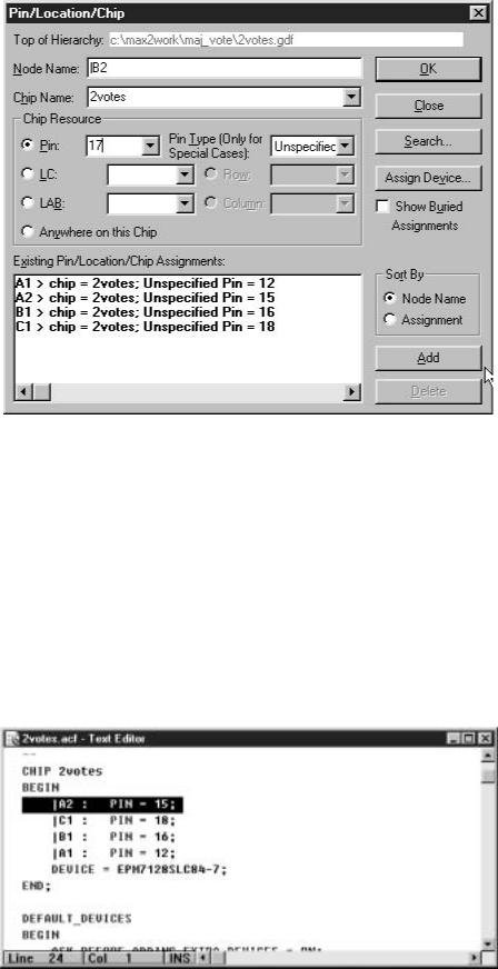
To assign a pin number, click on the pin to highlight it, then right-click to see the popup menu in Figure 4.35. Choose Assign, then Pin/Location/Chip. You could also do this from the Assign menu at the top of the screen.
142 C H A P T E R 4 • Introduction to PLDs and MAX+PLUS II
FIGURE 4.36
Pin/Location/Chip Assignment
Dialog Box
Table 4.2 Pin Assignment for a Majority Vote Circuit
Pin Name |
Pin Number |
|
|
A1 |
12 |
B1 |
16 |
C1 |
18 |
A2 |
15 |
B2 |
17 |
C2 |
21 |
Y |
4 |
|
|
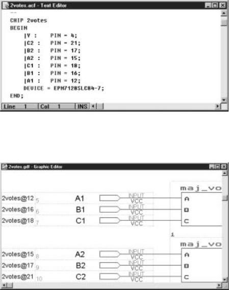
FIGURE 4.37
Pin Assignments in ACF (Before
Copying)
4.7 • Creating a Physical Design |
143 |
FIGURE 4.38
Pin Assignments in ACF (After Copying)
FIGURE 4.39
Pin Assignments as Seen in gdf File
We can assign pin numbers in the dialog box in Figure 4.36.
Type A1 in the Node Name box, 12 in the Pin box and click Add. Type B1 in the Node Name box, assign this name to pin 16, and click Add. Repeat this procedure until all names are assigned, as in Table 4.2. When all assignments are complete, click OK.
We can also assign pin numbers by editing the Assignment and Configuration File (acf), as shown in Figures 4.37 and 4.38. This technique works especially well if you need to assign pin numbers to a sequence of numerically related inputs and outputs.
Figure 4.37 shows the acf with four pin assignments made. We can add the others easily by using a copy-and-paste procedure. Highlight the line you wish to copy and copy it to the Windows clipboard (use Copy in the File menu or the Copy icon on the toolbar or Ctrl-C). Paste three copies into the acf and modify them so that they represent the remaining required pin assignments, as shown in Figure 4.38.
Figure 4.39 shows the input pin assignments as they appear in the gdf file.
144 C H A P T E R 4 • Introduction to PLDs and MAX+PLUS II
Programming CPLDs on the Altera UP-1 Circuit Board
K E Y T E R M S
ByteBlaster An Altera ribbon cable and connector used to program or configure
Altera CPLDs via the parallel port (LPT port) of an IBM PC or compatible.
JTAG Joint Test Action Group. A standards body that developed the format (called IEEE Std. 1149.1) for testing and programming devices while they are installed in a system.
ISP In-system programmability. The ability of a PLD (such as a MAX7000S) to be programmed without removing it from a circuit board.
ICR In-circuit reconfigurability. The ability of a PLD (such as a FLEX10K) to be configured without removing it from a circuit board.
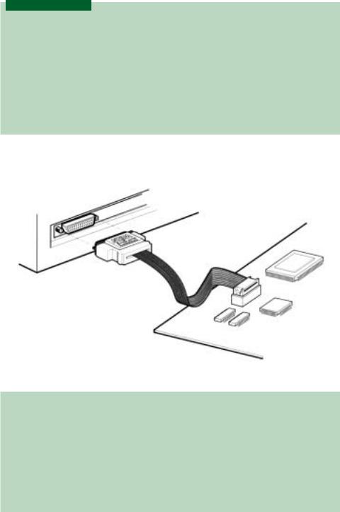
FIGURE 4.40
ByteBlaster Parallel Port Download Cable (By Permission of Altera Corporation)
TDI Test Data In. In a JTAG port, the serial input data to a device.
TDO Test Data Out. The JTAG signal, the serial output data from a device.
TMS Test Mode Select. The JTAG signal that controls the downloading of test or programming data.
TCK Test Clock. The JTAG signal that drives the JTAG downloading process from one state to the next.
JTAG Chain Multiple JTAG-compliant devices whose TDI and TDO ports form a continuous chain connection. Such a chain allows multi-device programming.
The CPLDs on the Altera UP-1 circuit board are programmed via the programming software in MAX PLUS II and a ribbon cable called the ByteBlaster. The ByteBlaster, shown in Figure 4.40, connects to the parallel port of a PC running MAX PLUS II to a 10-pin male socket that complies with the JTAG standard. This standard specifies a fourwire interface, originally developed for testing chips without removing them from a circuit board, but can also be used to program or configure PLDs.
4.7 • Creating a Physical Design |
145 |
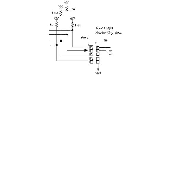
FIGURE 4.41
MAX9000, MAX7000S, and MAX7000A Programming with the ByteBlaster Cable (By Permission of Altera Corporation)
FIGURE 4.42
JTAG Chain Device Programming and Configuration with the ByteBlaster Cable (By Permission of Altera Corporation)
PLDs that can be programmed or configured while installed on a circuit board are called in-system programmable (ISP) or in-circuit reconfigurable (ICR). ISP is used to refer to nonvolatile devices, such as MAX7000S; ICR refers to volatile devices, such as FLEX10K.
The JTAG interface has four wires, as well as power and ground connections, as shown in Figure 4.41. Data are sent to a device from a JTAG controller (i.e., the PC) via the TDI (Test Data In) line. Data return from the device via TDO (Test Data Out). The data transfer is controlled by TMS (Test Mode Select). The process is driven from one step to the next by TCK (Test Clock).
Multiple devices can be programmed in a JTAG Chain, as shown in Figure 4.42. This connection allows both CPLDs on the Altera UP-1 Board to be programmed at the same time. The UP-1 board also has a female 10-pin socket labeled JTAG out, which allows two or more boards to be chained together. The choice of programming one or more CPLDs, or
146 C H A P T E R 4 • Introduction to PLDs and MAX+PLUS II
the CPLDs on one or more UP-1 boards, is determined by the placement of four on-board jumpers. These jumper positions are explained in the Altera University Program Design Laboratory Package User Guide. A copy of the User Guide is included in Appendix A for reference and is available at Altera’s Web site.
The operation of the JTAG port is controlled automatically by MAX PLUS II, so further details are not necessary at this time. For further information on the JTAG interface, refer to Altera Application Note 39, JTAG Boundary-Scan Testing in Altera Devices, in-
FIGURE 4.43
Hardware Setup Dialog Box
cluded in the Altera Documentation folder on the accompanying CD.
MAX PLUS II Programmer
To program a device on the Altera UP-1 board, set the jumpers to program the EPM7128S or configure the EPF10K20, as shown in the Altera University Program Design Laboratory Package User Guide. Connect the ByteBlaster cable from the parallel port of the PC running MAX PLUS II to the 10-pin JTAG header. (You may have to run a 25-wire cable
FIGURE 4.44
Programmer Dialog Box
(MAX7000S Device)
4.7 • Creating a Physical Design |
147 |
(male-D-connector-to-female-D-connector) to make it reach.) Plug an AC adapter (9-volt dc output) into the power jack of the UP-1 board.
Open the top-level file of the project you wish to download to the UP-1 board (e.g., maj_vote.gdf). Set the project to the current file. Invoke the MAX PLUS II Programmer from the MAX PLUS II menu or click the Programmer button (the icon showing the blue ribbon cable) on the MAX PLUS II toolbar.
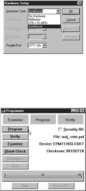
If you have never programmed a device with your copy of MAX PLUS II, you will need to set up the hardware configuration. Click Hardware Setup in the Options menu to
FIGURE 4.45
JTAG Menu
FIGURE 4.46
Multi-Device JTAG Chain Setup
get the dialog box in Figure 4.43.
Select ByteBlaster in the Hardware Type box. Ensure that Parallel Port is the same as the port the ByteBlaster is plugged into (usually LPT1:). Click OK. (If you have a choice, configure your parallel port as an Enhanced Communications Port (ECP) in your computer’s CMOS setup. For most users this step is not necessary, as the port is already configured this way.)
148 C H A P T E R 4 • Introduction to PLDs and MAX+PLUS II
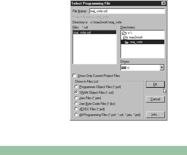
FIGURE 4.47
Select Programming File Dialog Box
If the current project was compiled with the MAX7000S device selected, the pof file
for the project will automatically be available. The Programmer dialog box will appear as in Figure 4.44. To download, click Program.
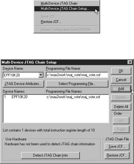
If the project was compiled for the FLEX10K device and the device is to be configured via a ByteBlaster, it must be configured via the
Multi-Device JTAG Chain available in the JTAG menu. Select the JTAG menu, shown in Figure 4.45, and choose
Multi-Device JTAG
Chain Setup.
In the Multi-Device JTAG Chain Setup window, shown in Figure 4.46, select the pulldown menu for the device name. Select
EPF10K20. Choose
Delete All to clear the box of any previous programming file names. Choose the Select Programming File button.
The Select Programming File dialog box will appear, as in Figure 4.47. Find and se-
lect |
the |
file |
drive:\max2work\maj_v

ote\maj_vote.sof. Click
OK. Choose the Add button in the JTAG setup box to add the SRAM Object File (sof) to the list. Choose the Detect JTAG Chain Info button to set up the hardware for programming. Choose
OK. Click the Configure button in the Programmer dialog box to download the binary information to the FLEX10K CPLD on the UP-1
board.
S U M M A R Y
1.A programmable logic device (PLD) is a digital device that is shipped blank and whose function is determined by the end user.
2.PLDs offer design flexibility, reduce board space and package count, and can be used to develop digital designs more quickly than fixed-function logic.
3.Some types of PLDs include PAL (programmable array logic), GAL (generic array logic), EPLD (erasable PLD), CPLD (complex PLD), FPGA (field-programmable gate array).
4.Complex PLDs (CPLDs) are devices with several programmable sections that are interconnected inside the chip.
5.PLD design and programming requires special software, such as Altera’s MAX PLUS II.
6.PLD designs can be entered by schematic capture (Graphic Design Files) or text-based languages, such as Altera Hardware Description Language (AHDL) and VHSIC Hardware Description Language (VHDL).
7.MAX PLUS II organizes PLD design files in a project. Since many operations in MAX PLUS II are performed on a project, you should set the project to the current file (File menu) whenever you change windows and make a modification to a design file.
8.Save your work every time you pause for thought.
9.A MAX PLUS II Graphic Design File (gdf) consists of graphical symbols of components that are interconnected by lines drawn between inputs and outputs of the components.
10.Circuit inputs and outputs in a gdf have special symbols. The input and output pins must be named, but need not be numbered in the first stages of a design.
ship between the inputs and outputs.
22.The entity declaration defines ports (inputs and outputs) and the type of each port (the range of values each port can have).
23.Some common types are BIT (0 or 1), STD_LOGIC (ninevalued standard logic), and INTEGER (whole numbers).
24.The STD_LOGIC type can take on any of the following values:
‘U’,— — Uninitialized
Glossary 149
11.The MAX PLUS II compiler translates the design information from a gdf or text file into binary data that can be downloaded into a PLD. For a MAX7000S, the compiler generates a Programmer Object File (pof) to program the device. For a FLEX10K, an SRAM Object File (sof) is generated to configure the device.
12.MAX7000S devices are nonvolatile; they stay programmed when the power is removed from the chip. FLEX10K devices are volatile; they lose their programming data when power is removed.
13.If a CPLD part number is not specified, the MAX PLUS II compiler will automatically select one. It is good practice to assign the part number of the device before compiling, as this can affect the accuracy of certain parts of the design process, such as simulation. The CPLDs on the Altera UP-1 board are EPM7128SLC84-7 and EPF10K20RC240-4.
14.Some useful compiler options are: Design Doctor (checks for good design practice), Timing SNF Extractor (compiles data required for timing simulations), and Smart Recompile (allows part of the compile process to be skipped if only part of a design has changed).
15.Compiler messages can be in green text (Info), blue text (Warning; possible problems, but not fatal), or red text (Error; fatal, compiling stops).
16.MAX PLUS II files can be arranged in a design hierarchy. That is, a MAX PLUS II file can contain components that are complete MAX PLUS II designs in and of themselves.
17.A file that contains other designs, but is not part of a higherlevel design, is called the top level of a hierarchy.
18.If the top level of a hierarchy is a gdf, lower-level designs are embedded in the gdf as default symbols that are created from the original design files of the components.
19.MAX PLUS II looks for default symbols in the present working directory, then in the directories specified as user libraries.
20.VHDL (VHSIC Hardware Description Language) is a textbased programming language used to model and program digital circuits.
21.Every VHDL file requires an entity declaration, which describes the external aspects of the design (inputs and outputs), and an architecture body, which describes the relation-
‘X’,— — Forcing |
Unknown |
|
‘0’,— — |
Forcing |
0 |
‘1’,— — |
Forcing |
1 |
‘Z’,— — High |
Impedance |
|
‘W’,— — Weak |
Unknown |
|
‘L’,— — |
Weak |
0 |
‘H’,— — |
Weak |
1 |