

Digital design with CPLD applications and VHDL (R. Dueck, 2000)
.pdf30 C H A P T E R 2 • Logic Functions and Gates
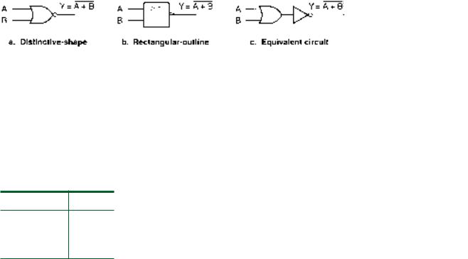
FIGURE 2.8
Example 2.1
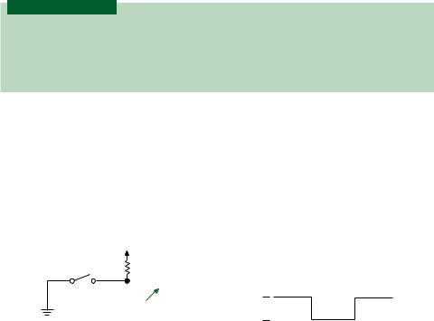
2.One or more switches closed will turn on the lamp. This OR function is shown in Figure 2.8b.
3.Two switches are required to activate a punch press, as shown in Figure 2.8c. This is an AND function.
Key switch |
Key switch |
|
(manager) |
(employee) |
|
DC |
Electronic |
|
voltage |
||
lock |
||
source |
||
|
a. Two keys to open a safe (AND)
|
Door switch A |
AC |
|
voltage |
Lamp |
source |
Door switch B |
|
b. One or more switches turn on a lamp (OR)
Hand |
Hand |
|
switch A |
switch B |
|
AC |
Solenoid |
|
voltage |
||
(punch) |
||
source |
||
|
c. Two switches are required to activate a punch press (AND)
Active Levels
K E Y T E R M S
Active level A logic level defined as the “ON” state for a particular circuit input or output. The active level can be either HIGH or LOW.
Active HIGH An active-HIGH terminal is considered “ON” when it is in the logic HIGH state. Indicated by the absence of a bubble at the terminal in distinc- tive-shape symbols.
Active LOW An active-LOW terminal is considered “ON” when it is in the logic LOW state. Indicated by a bubble at the terminal in distinctive-shape symbols.
An active level of a gate input or output is the logic level, either HIGH or LOW, of the terminal when it is performing its designated function. An active LOW is shown by a bubble or an arrow symbol on the affected terminal. If there is no bubble or arrow, we assume the terminal is active HIGH.
2.2 • Logic Switches and LED Indicators |
31 |
The AND function has active-HIGH inputs and an active-HIGH output. To make the output HIGH, inputs A AND B must both be HIGH. The gate performs its designated function only when all inputs are HIGH.
The OR gate requires input A OR input B to be HIGH for its output to be HIGH. The HIGH active levels are shown by the absence of bubbles or arrows on the terminals.
SECTION REVIEW PROBLEM FOR SECTION 2.1
A 4-input gate has input variables A, B, C, and D and output Y. Write a descriptive sentence for the active output state(s) if the gate is
2.1AND;
2.2OR.
2.2Logic Switches and LED Indicators
Before continuing on, we should examine a few simple circuits that can be used for input or output in a digital circuit. Single-pole single-throw (SPST) and pushbutton switches can be used, in combination with resistors, to generate logic voltages for circuit inputs. Light emitting diodes (LEDs) can be used to monitor outputs of circuits.
Logic Switches
K E Y T E R M S
VCC The power supply voltage in a transistor-based electronic circuit. The term often refers to the power supply of digital circuits.
Pull-up resistor A resistor connected from a point in an electronic circuit to the power supply of that circuit.
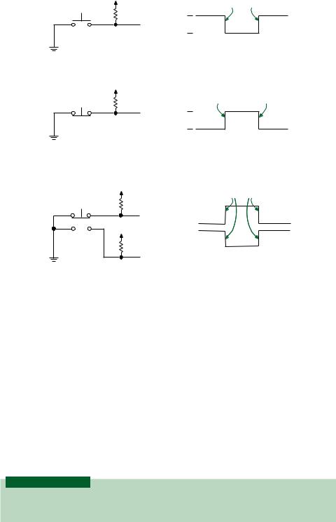
Figure 2.9a shows a single-pole single-throw (SPST) switch connected as a logic switch. An important premise of this circuit is that the input of the digital circuit to which it is connected has a very high resistance to current. When the switch is open, the current flowing through the pull-up resistor from VCC to the digital circuit is very small. Since the current is small, Ohm’s law states that very little voltage drops across the pull-up resistor; the voltage is about the same at one end as at the other. Therefore, an open switch generates a logic HIGH at point X.
Vcc
|
|
|
X |
Digital |
|
High |
|
circuit |
1 |
||
|
|
||||
|
|
|
|||
|
|
|
|||
input |
|
|
Open Closed Open |
||
resistance |
|
0 |
|||
a. Circuit |
|
|
b. Logic levels |
||
FIGURE 2.9
SPST Logic Switch
When the switch is closed, the majority of current flows to ground, limited only by the value of the pull-up resistor. (Since a pull-up resistor is typically between 1 k and 10 k , the LOW-state current in the resistor is about 0.5 mA to 5 mA.) Point X is approximately at ground potential, or logic LOW. Thus the switch generates a HIGH when open and a LOW when closed. The pull-up resistor provides a connection to VCC in the HIGH state
32 C H A P T E R 2 • Logic Functions and Gates
and limits power supply current in the LOW state. Figure 2.9b shows the voltage levels when the switch is closed and when it is open.
Figure 2.10 shows how pushbuttons can be used as logic inputs. Figure 2.10a shows a normally open pushbutton and a pull-up resistor. The pushbutton has a spring-loaded plunger that makes a connection between two internal contacts when pressed. When released, the spring returns the plunger to the “normal” (open) state. The logic voltage at X is normally HIGH, but LOW when the button is pressed.
Vcc
Press Release
1
X
0
a. Normally open pushbutton
Press Release
X 1
0
b. Normally closed pushbutton
Vcc
Press Release
COM |
N.C. |
X |
X
N.O. Vcc
Y
Y
c. Two-pole pushbutton
FIGURE 2.10
Pushbuttons as Logic Switches
Figure 2.10b shows a normally closed pushbutton. The internal spring holds the plunger so that the connection is normally made between the two contacts. When the button is pressed, the connection is broken and the resistor pulls up the voltage at X to a logic HIGH. At rest, X is grounded and the voltage at X is LOW.
It is sometimes desirable to have normally HIGH and normally LOW levels available from the same switch. The two-pole pushbutton in Figure 2.10c provides such a function. The switch has a normally open and a normally closed contact. One contact of each switch is connected to the other, in an internal COMMON connection, allowing the switch to have three terminals rather than four. The circuit has two pull-up resistors, one for X and one for Y. X is normally HIGH and goes LOW when the switch is pressed. Y is opposite.
LED Indicators
K E Y T E R M S
LED Light-emitting diode. An electronic device that conducts current in one di-
rection only and illuminates when it is conducting.
2.2 • Logic Switches and LED Indicators |
33 |
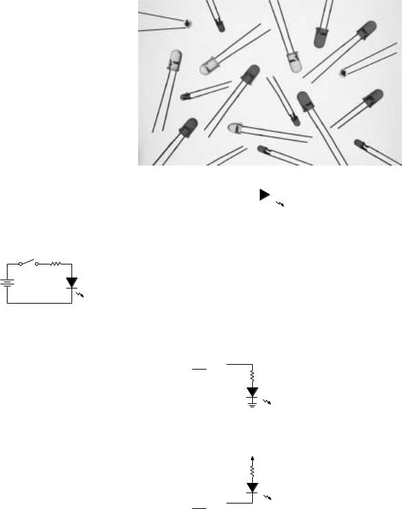
A device used to indicate the status of a digital output is the light-emitting diode or LED. This is sometimes pronounced as a word (“led”) and sometimes said as separate initials (“ell ee dee”). This device comes in a variety of shapes, sizes, and colors, some of which are shown in the photo of Figure 2.11. The circuit symbol, shown in Figure 2.12, has two terminals, called the anode (positive) and cathode (negative). The arrow coming from the symbol indicates emitted light.
FIGURE 2.11
LEDs
470
Vcc
FIGURE 2.13
Condition for LED Illumination
FIGURE 2.14
AND Gate Driving an LED
Anode |
Cathode |
||
|
|
|
|
|
|
|
|
FIGURE 2.12
Light-Emitting Diode (LED)
The electrical requirements for the LED are simple: current flows through the LED if the anode is more positive than the cathode by more than a specified value (about 1.5 volts). If enough current flows, the LED illuminates. If more current flows, the illumination is brighter. (If too much flows, the LED burns out, so a series resistor is used to keep the current in the required range.) Figure 2.13 shows a circuit in which an LED illuminates when a switch is closed.
Figure 2.14 shows an AND gate driving an LED. In Figure 2.14a, the LED is on when Y is HIGH (5 volts), since the anode of the LED is more positive than the cathode.
A  Y
Y
B
470
a. LED on when Y is HIGH
Vcc
470
A  Y
Y
B
b. LED on when Y is LOW
34 C H A P T E R 2 • Logic Functions and Gates
Vcc
Vcc
470
1k
S1
FIGURE 2.15
LED Indicates Status of Switch
In Figure 2.14b, the LED turns on when Y is LOW (0 volts), again since the anode is more positive than the cathode.
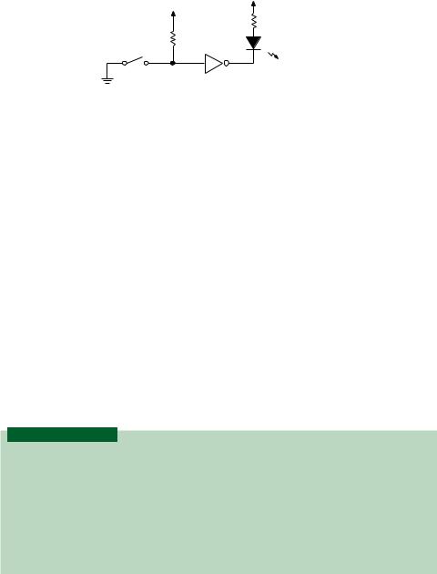
Figure 2.15 shows a circuit in which an LED indicates the status of a logic switch. When the switch is open, the 1 k pull-up applies a HIGH to the inverter input. The inverter output is LOW, turning on the LED (anode is more positive than cathode). When the switch is closed, the inverter input is LOW. The inverter output is HIGH (same value as VCC), making anode and cathode voltages equal. No current flows through the LED, and it is therefore off. Thus, the LED is on for a HIGH state at the switch and off for a LOW. Note, however, that the LED is on when the inverter output is LOW.
SECTION 2.2 REVIEW PROBLEM
2.3A single-pole single-throw switch is connected such that one end is grounded and one end is connected to a 1 k pull-up resistor. The other end of the resistor connects to
the circuit power supply, VCC. What logic level does the switch provide when it is open? When it is closed?
2.3Derived Logic Functions
K E Y T E R M S
NAND gate A logic circuit whose output is LOW when all inputs are HIGH.
NOR gate A logic circuit whose output is LOW when at least one input is HIGH.
Exclusive OR gate A 2-input logic circuit whose output is HIGH when one input (but not both) is HIGH.
Exclusive NOR gate A 2-input logic circuit whose output is the complement of an Exclusive OR gate.
Coincidence gate An Exclusive NOR gate.
The basic logic functions, AND, OR, and NOT, can be combined to make any other logic function. Special logic gates exist for several of the most common of these derived functions. In fact, for reasons we will discover later, two of these derived-function gates, NAND and NOR, are the most common of all gates, and each can be used to create any logic function.
NAND and NOR Functions
The names NAND and NOR are contractions of NOT AND and NOT OR, respectively.
The NAND is generated by inverting the output of an AND function. The symbols for the
NAND gate and its equivalent circuit are shown in Figure 2.16.
The algebraic expression for the NAND function is:
Y A B
2.3 • Derived Logic Functions |
35 |
FIGURE 2.16
NAND Gate Symbols
Table 2.6 NAND Function
Truth Table
A |
B |
Y |
|
|
|
0 |
0 |
1 |
0 |
1 |
1 |
1 |
0 |
1 |
1 |
1 |
0 |
|
|
|
Table 2.7 NOR Function
Truth Table
A B Y
0 0 1
0 1 0
1 0 0
1 1 0
The entire function is inverted because the bubble is on the NAND gate output. Table 2.6 shows the NAND gate truth table. The output is LOW when A AND B are
HIGH.
We can generate the NOR function by inverting the output of an OR gate. The NOR function truth table is shown in Table 2.7. The truth table tells us that the output is LOW when A OR B is HIGH.
Figure 2.17 shows the logic symbols for the NOR gate.
FIGURE 2.17
NOR Gate Symbols
The algebraic expression for the NOR function is:
Y A B
The entire function is inverted because the bubble is on the gate output.
We know that the outputs of both gates are active LOW because of the bubbles on the output terminals. The inputs are active HIGH because there are no bubbles on the input terminals.
Multiple-Input NAND and NOR Gates
Table 2.8 shows the truth tables of the 3-input NAND and NOR functions. The logic circuit symbols for these gates are shown in Figure 2.18.
Table 2.8 3-input NAND and NOR Function Truth Tables
A |
B |
C |
A B C |
A B C |
|
|
|
|
|
0 |
0 |
0 |
1 |
1 |
0 |
0 |
1 |
1 |
0 |
0 |
1 |
0 |
1 |
0 |
0 |
1 |
1 |
1 |
0 |
1 |
0 |
0 |
1 |
0 |
1 |
0 |
1 |
1 |
0 |
1 |
1 |
0 |
1 |
0 |
1 |
1 |
1 |
0 |
0 |
|
|
|
|
|
The truth tables of these gates can be generated by understanding the active levels of the gate inputs and outputs. The NAND output is LOW when A AND B AND C are HIGH. This is shown in the last line of the NAND truth table. The NOR output is LOW if one or more of A OR B OR C is HIGH. This describes all lines of the NOR truth table except the first.
36 C H A P T E R 2 • Logic Functions and Gates
FIGURE 2.18
3-Input NAND and NOR Gates
Exclusive OR and Exclusive NOR Functions
The Exclusive OR function (abbreviated XOR) is a special case of the OR function. The output of a 2-input XOR gate is HIGH when one and only one of the inputs is HIGH. (Multiple-input XOR circuits do not expand as simply as other functions. As we will see in a later chapter, an XOR output is HIGH when an odd number of inputs is HIGH.)
Unlike the OR gate, which is sometimes called an Inclusive OR, a HIGH at both inputs makes the output LOW. (We could say that the case in which both inputs are HIGH is excluded.)
The gate symbol for the Exclusive OR gate is shown in Figure 2.19.
Table 2.9 Exclusive OR
Function Truth Table
A B Y
0 0 0
0 1 1
1 0 1
1 1 0
FIGURE 2.19
Exclusive OR Gate
Table 2.9 shows the truth table for the XOR function.
Another way of looking at the Exclusive OR gate is that its output is HIGH when the inputs are different and LOW when they are the same. This is a useful property in some applications, such as error detection in digital communication systems. (Transmitted data can be compared with received data. If they are the same, no error has been detected.)
The XOR function is expressed algebraically as:
Y A B
The Exclusive NOR function is the complement of the Exclusive OR function and shares some of the same properties. The symbol, shown in Figure 2.20, is an XOR gate
FIGURE 2.20
Exclusive NOR Gate
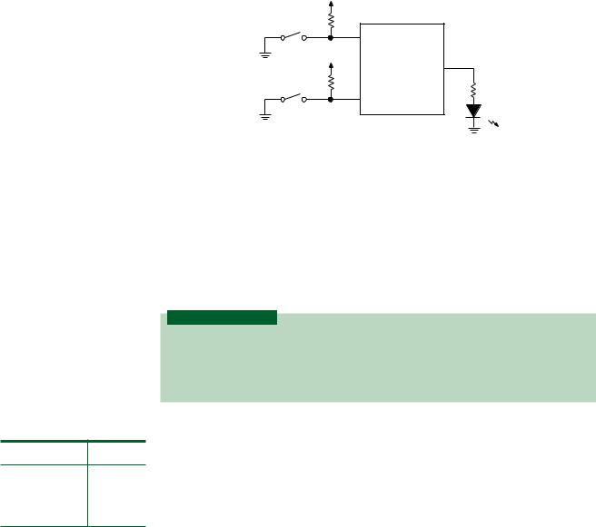
Table 2.10 Exclusive NOR
Function Truth Table
A |
B |
Y |
|
|
|
0 |
0 |
1 |
0 |
1 |
0 |
1 |
0 |
0 |
1 |
1 |
1 |
|
|
|
2.4 • DeMorgan’s Theorems and Gate Equivalence |
37 |
with a bubble on the output, implying that the entire function is inverted. Table 2.10 shows the Exclusive NOR truth table.
The algebraic expression for the Exclusive NOR function is:
Y A B
The output of the Exclusive NOR gate is HIGH when the inputs are the same and LOW when they are different. For this reason, the XNOR gate is also called a coincidence gate. This same/different property is similar to that of the Exclusive OR gate, only opposite in sense. Many of the applications that make use of this property can use either the XOR or the XNOR gate.
SECTION 2.3 REVIEW PROBLEMS
The output of a logic gate turns on an LED when it is HIGH. The gate has two inputs, each of which is connected to a logic switch, as shown in Figure 2.21.
Vcc
A
Vcc
Logic gate Y
B
FIGURE 2.21
Section Review Problems: Logic Gate Properties
2.4What type of gate will turn on the light when the switches are in opposite positions?
2.5Which gate will turn off the light only when both switches are HIGH?
2.6What type of gate turns on the light only when both switches are LOW?
2.7Which gate turns on the light when the switches are in the same position?
2.4DeMorgan’s Theorems and Gate Equivalence
K E Y T E R M S
Table 2.11 NAND Truth
Table
A B Y
0 0 1
0 1 1
1 0 1
1 1 0
DeMorgan’s theorems Two theorems in Boolean algebra that allow us to transform any gate from an AND-shaped to an OR-shaped gate and vice versa.
DeMorgan equivalent forms Two gate symbols, one AND-shaped and one ORshaped, that are equivalent according to DeMorgan’s theorems.
Recall the truth table (repeated in Table 2.11) and description of a 2-input NAND gate. “Output Y is LOW if inputs A AND B are HIGH.” Or, “Output Y is LOW if all inputs are HIGH.” The condition of this sentence is satisfied in the last line of Table 2.11.
We could also describe the gate function by saying, “Output Y is HIGH if A OR B (OR both) are LOW,” or, “The output is HIGH if at least one input is LOW.” These conditions are satisfied by the first three lines of Table 2.11.
The gates in Figure 2.22 represent positiveand negative-logic forms of a NAND gate. Figure 2.23 shows the logic equivalents of these gates. In the first case, we combine the in-
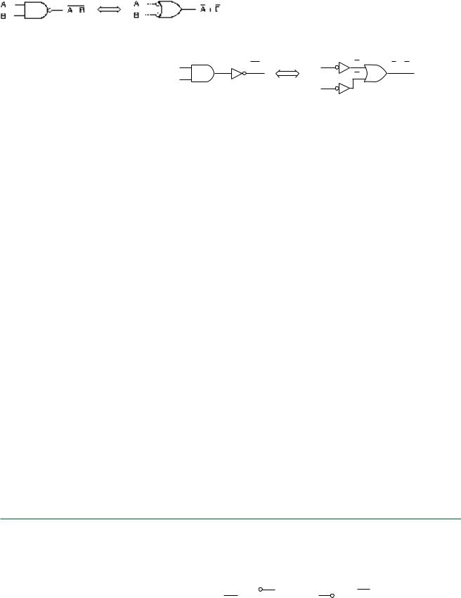
38 C H A P T E R 2 • Logic Functions and Gates
FIGURE 2.22
NAND Gate and DeMorgan Equivalent
A |
AB |
AB |
A |
A B |
|
|
A |
|
|
B |
|
|
B |
|
|
|
|
B |
|
|
a. AND then invert |
|
b. Invert then OR |
|
FIGURE 2.23
Logic Equivalents of Positive and Negative NAND Gates
puts in an AND function, then invert the result. In the second case, we invert the variables, then combine the inverted inputs in an OR function.
The Boolean function for the AND-shaped gate is given by:
Y A B
The Boolean expression for the OR-shaped gate is:
Y A B
The gates shown in Figure 2.22 are called DeMorgan equivalent forms. Both gates have the same truth table, but represent different aspects or ways of looking at the NAND function. We can extend this observation to state that any gate (except XOR and XNOR) has two equivalent forms, one AND, one OR.
A gate can be categorized by examining three attributes: shape, input, and output. A question arises from each attribute:
1.What is its shape (AND/OR)? AND: all
OR: at least one
2.What active level is at the gate inputs (HIGH/LOW)?
3.What active level is at the gate output (HIGH/LOW)?
The answers to these questions characterize any gate and allow us to write a descriptive sentence and a truth table for that gate. The DeMorgan equivalent forms of the gate will yield opposite answers to each of the above questions.
Thus the gates in Figure 2.22 have the following complementary attributes:
|
Basic Gate |
DeMorgan Equivalent |
Boolean Expression |
A B |
A B |
Shape |
AND |
OR |
Input Active Level |
HIGH |
LOW |
Output Active Level |
LOW |
HIGH |
EXAMPLE 2.2
FIGURE 2.24
Example 2.2 Logic Gates
Analyze the shape, input, and output of the gates shown in Figure 2.24 and write a Boolean expression, a descriptive sentence, and a truth table of each one. Write an asterisk beside the active output level on each truth table. Describe how these gates relate to each other.
A  Y A
Y A 
 Y
Y
B B
a. |
b. |

2.4 • DeMorgan’s Theorems and Gate Equivalence |
39 |
SOLUTION
a.Boolean expression: Y A B
Shape: OR (at least one)
Input: HIGH Output: LOW
Descriptive sentence: Output Y is LOW if A OR B is HIGH.
Truth table: |
Table 2.12 |
Truth Table |
|
|
of Gate in Figure 2.24a. |
||
|
|
|
|
|
A |
B |
Y |
|
|
|
|
|
0 |
0 |
1 |
|
0 |
1 |
0* |
|
1 |
0 |
0* |
|
1 |
1 |
0* |
|
|
|
|
b.Boolean expression: Y A B
Shape: AND (all)
Input: LOW Output: HIGH
Descriptive sentence: Output Y is HIGH if A AND B are LOW.
Truth table: |
Table 2.13 |
Truth Table |
|
|
of Gate in Figure 2.124b. |
||
|
|
|
|
|
A |
B |
Y |
|
|
|
|
|
0 |
0 |
1* |
|
0 |
1 |
0 |
|
1 |
0 |
0 |
|
1 |
1 |
0 |
|
|
|
|
Both gates in this example yield the same truth table. Therefore they are DeMorgan
equivalents of one another (positiveand negative-NOR gates). |
|
|
The gates in Figures 2.22 and 2.24 yield the following algebraic equivalencies:
A B A BA B A B
These equivalencies are known as DeMorgan’s theorems. (You can remember how to use DeMorgan’s theorems by a simple rhyme: “Break the line and change the sign.”)
It is tempting to compare the first gate in Figure 2.22 and the second in Figure 2.24 and declare them equivalent. Both gates are AND-shaped, both have inversions. However, the comparison is false. The gates have different truth tables, as we have found in Tables 2.11 and 2.13. Therefore they have different logic functions and are not equivalent. The same is true of the OR-shaped gates in Figures 2.22 and 2.24. The gates may look similar, but since they have different truth tables, they have different logic functions and are therefore not equivalent.
The confusion arises when, after changing the logic input and output levels, you forget to change the shape of the gate. This is a common, but serious, error. These inequalities can be expressed as follows:
A B A BA B A B