

Digital design with CPLD applications and VHDL (R. Dueck, 2000)
.pdf20 C H A P T E R 1 • Basic Principles of Digital Systems
Pulse width: 50% of leading edge to 50% of trailing edge. |
|
tw 25 s 5 s 20 s |
|
Rise time: 10% of rising edge to 90% of rising edge. |
|
tr 8 s 2 s 6 s |
|
Fall time: 90% of falling edge to 10% of falling edge. |
|
tf 30 s 20 s 10 s |
|
|
SECTION 1.5 REVIEW PROBLEMS
A digital circuit produces a waveform that can be described by the following periodic bit pattern: 0011001100110011.
1.12What is the duty cycle of the waveform?
1.13Write the bit pattern of a waveform with the same duty cycle and twice the frequency of the original.
1.14Write the bit pattern of a waveform having the same frequency as the original and a duty cycle of 75%.
S U M M A R Y
1.The two basic areas of electronics are analog and digital electronics. Analog electronics deals with continuously variable quantities; digital electronics represents the world in discrete steps.
2.Digital logic uses defined voltage levels, called logic levels, to represent binary numbers within an electronic system.
3.The higher voltage in a digital system represents the binary digit 1 and is called a logic HIGH or logic 1. The lower voltage in a system represents the binary digit 0 and is called a logic LOW or logic 0.
4.The logic levels of multiple locations in a digital circuit can be combined to represent a multibit binary number.
5.Binary is a positional number system (base 2) with two digits, 0 and 1, and positional multipliers that are powers of 2.
6.The bit with the largest positional weight in a binary number is called the most significant bit (MSB); the bit with the smallest positional weight is called the least significant bit (LSB). The MSB is also the leftmost bit in the number; the LSB is the rightmost bit.
7.A decimal number can be converted to binary by sum of powers of 2 (add place values to get a total) or repeated division by 2 (divide by 2 until quotient is 0; remainders are the binary value).
8.The hexadecimal number system is based on 16. It uses 16 digits, from 0–9 and A–F, with power-of-16 multipliers.
9.Each hexadecimal digit uniquely corresponds to a 4-bit binary value. Hex digits can thus be used as shorthand for binary.
10.A digital waveform is a sequence of bits over time. A waveform can be periodic (repetitive), aperiodic (nonrepetitive), or pulsed (a single variation and return between logic levels.)
11.Periodic waveforms are measured by period (T: time for one
cycle), time HIGH (th), time LOW (tl), frequency ( f: number of cycles per second), and duty cycle (DC or %DC: fraction of cycle in HIGH state).
12.Pulse waveforms are measured by pulse width (tw: time from 50% of leading edge of 50% of trailing edge), rise time (tr: time from 10% to 90% of rising edge) and fall time (tf: time from 90% to 10% of falling edge).
G L O S S A R Y
Amplitude The instantaneous voltage of a waveform. Often used to mean maximum amplitude, or peak voltage, of a pulse.
Analog A way of representing some physical quantity, such as temperature or velocity, by a proportional continuous voltage or current. An analog voltage or current can have any value within a defined range.
Aperiodic waveform A time-varying sequence of logic HIGHs and LOWs that does not repeat.
Binary number system A number system used extensively in digital systems, based on the number 2. It uses two digits to write any number.
Bit Binary digit. A 0 or a 1.

Problems 21
Continuous Smoothly connected. An unbroken series of consecutive values with no instantaneous changes.
Digital A way of representing a physical quantity by a series of binary numbers. A digital representation can have only specific discrete values.
Digital waveform A series of logic 1s and 0s plotted as a function of time.
Discrete Separated into distinct segments or pieces. A series of discontinous values.
Duty cycle (DC) Fraction of the total period that a digital waveform is in the HIGH state. DC th/T (often expressed as a percentage: %DC th/T 100%).
Edge The part of the pulse that represents the transition from one logic level to the other.
Fall time (tf) Elapsed time from the 90% point to the 10% point of the falling edge of a pulse.
Falling edge The part of a pulse where the logic level is in transition from a HIGH to a LOW.
Frequency ( f ) Number of times per second that a periodic waveform repeats. f 1/T Unit: Hertz (Hz).
Hexadecimal number system Base-16 number system. Hexadecimal numbers are written with sixteen digits, 0–9 and A–F, with power-of-16 positional multipliers.
Leading edge The edge of a pulse that occurs earliest in time.
Least significant bit (LSB) The rightmost bit of a binary number. This bit has the number’s smallest positional multiplier.
Logic HIGH The higher of two voltages in a digital system with two logic levels.
Logic level A voltage level that represents a defined digital state in an electronic circuit.
Logic LOW The lower of two voltages in a digital system with two logic levels.
Most significant bit (MSB) The leftmost bit in a binary number. This bit has the number’s largest positional multiplier.
Negative logic A system in which logic LOW represents binary digit 1 and logic HIGH represents binary digit 0.
Period (T) Time required for a period waveform to repeat. Unit: seconds (s).
Periodic waveform A time-varying sequence of logic HIGHs and LOWs that repeats over a specified period of time.
Positional notation A system of writing numbers in which the value of a digit depends not only on the digit, but also on its placement within a number.
Positive logic A system in which logic LOW represents binary digit 0 and logic HIGH represents binary digit 1.
Pulse A momentary variation of voltage from one logic level to the opposite level and back again.
Pulse width (tw) Elapsed time from the 50% point of the leading edge of a pulse to the 50% point of the trailing edge.
Radix point The generalized form of a decimal point. In any positional number system, the radix point marks the dividing line between positional multipliers that are positive and negative powers of the system’s number base.
Rise time (tr) Elapsed time from the 10% point to the 90% point of the rising edge of a pulse.
Rising edge The part of a pulse where the logic level is in transition from a LOW to a HIGH.
Time HIGH (th) Time during one period that a waveform is in the HIGH state. Unit: seconds (s).
Time LOW (tl ) Time during one period that a waveform is in the LOW state. Unit: seconds (s).
Trailing edge The edge of a pulse that occurs latest in time.
P R O B L E M S
Problem numbers set in color indicate more difficult problems: those with underlines indicate most difficult problems.
Section 1.1 Digital Versus Analog Electronics
1.1Which of the following quantities is analog in nature and which digital? Explain your answers.
a.Water temperature at the beach
b.Weight of a bucket of sand
c.Grains of sand in a bucket
d.Waves hitting the beach in one hour
e.Height of a wave
f.People in a square mile
Section 1.2 Digital Logic Levels
1.2A digital logic system is defined by the voltages 3.3 volts and 0 volts. For a positive logic system, state which voltage corresponds to a logic 0 and which to a logic 1.
Section 1.3 The Binary Number System
1.3Calculate the decimal values of each of the following binary numbers:
a. |
100 |
f. |
11101 |
b. |
1000 |
g. |
111011 |
c. |
11001 |
h. |
1011101 |
d. |
110 |
i. |
100001 |
e. |
10101 |
j. |
10111001 |
1.4Translate each of the following combinations of HIGH
(H) and LOW (L) logic levels to binary numbers using positive logic:
a. H H L H |
d. L L L H |
b. L H L H |
e. H L L L |
c. H L H L |
|

22 |
C H A P T E R 1 • Basic Principles of Digital Systems |
1.5List the sequence of binary numbers from 101 to 1000.
1.6List the sequence of binary numbers from 10000 to 11111.
1.7What is the decimal value of the most significant bit for the numbers in Problem 1.6
1.8Convert the following decimal numbers to binary. Use the sum-of-powers-of-2 method for parts a, c, e, and g. Use the repeated-division-by-2 method for parts b, d, f, and h.
a. |
7510 |
e. |
6310 |
b. |
8310 |
f. |
6410 |
c. |
23710 |
g. |
408710 |
d. |
19810 |
h. |
819310 |
1.9Convert the following fractional binary numbers to their decimal equivalents.
a.0.101
b.0.011
c.0.1101
1.10Convert the following fractional binary numbers to their decimal equivalents.
a. |
0.01 |
c. |
0.010101 |
b. |
0.0101 |
d. |
0.01010101 |
1.11The numbers in Problem 1.10 are converging to a closer and closer binary approximation of a simple fraction that can be expressed by decimal integers a/b. What is the fraction?
1.12What is the simple decimal fraction (a/b) represented by the repeating binary number 0.101010 . . . ?
1.13Convert the following decimal numbers to their binary equivalents. If a number has an integer part larger than 0, calculate the integer and fractional parts separately.
a. |
0.7510 |
e. |
1.7510 |
b. |
0.62510 |
f. |
3.9510 |
c. |
0.187510 |
g. |
67.8410 |
d. |
0.6510 |
|
|
mal equivalents.
a.70910
b.188910
c.409510
d.409610
e.1012810
f.3200010
g.3276810
1.18Convert the following hexadecimal numbers to their binary equivalents.
a.F3C8H
b.D3B4H
c.8037H
d.FABDH
e.30ACH
f.3E7B6H
g.743DCFH
1.19Convert the following binary numbers to their hexadecimal equivalents.
a.1011110100001102
b.1011011010102
c.1100010110112
d.1101011110001002
e.101010111100001012
f.110011000101101112
g.1010000000000000002
Section 1.5 Digital Waveforms
1.20Calculate the time LOW, time HIGH, period, frequency, and percent duty cycle for the waveforms shown in Figure 1.12. How are the waveforms similar? How do they differ?
1.21Which of the waveforms in Figure 1.13 are periodic and which are aperiodic? Explain your answers.
Section 1.4 Hexadecimal Numbers
1.14Write all the hexadecimal numbers in sequence from 308H to 321H inclusive.
1.15Write all the hexadecimal numbers in sequence from 9F7H to A03H inclusive.
1.16Convert the following hexadecimal numbers to their decimal equivalents.
a. |
1A0H |
e. |
F3C8H |
b. |
10AH |
f. |
D3B4H |
c. |
FFFH |
g. |
C000H |
d. |
1000H |
h. |
30BAFH |
1.17Convert the following decimal numbers to their hexadeci-
1.22Sketch the pulse waveforms represented by the following strings of 0s and 1s. State which waveforms are periodic and which are aperiodic.
a.11001111001110110000000110110101
b.111000111000111000111000111000111
c.11111111000000001111111111111111
d.01100110011001100110011001100110
e.011101101001101001011010011101110
1.23Calculate the pulse width, rise time, and fall time of the pulse shown in Figure 1.14.
1.24Repeat Problem 1.23 for the pulse shown in Figure 1.15.

Answers To Section Review Problems |
23 |
FIGURE 1.12
Problem 1.20: Periodic
Waveforms
FIGURE 1.13
Problem 1.21: Aperiodic and
Periodic Waveforms
|
|
|
|
FIGURE 1.14 |
FIGURE 1.15 |
||
Problem 1.23: Pulse |
Problem 1.24: Pulse |
||
A N S W E R S T O S E C T I O N R E V I E W P R O B L E M S
Section 1.1
1.1 An analog audio system makes a direct copy of the recorded sound waves. A digital system stores the sound as a series of binary numbers.
Section 1.3
1.2 |
64; |
1.3. 128; |
1.4. 1010000, 1010001, 1010010, |
|
1010011, 1010100, 1010101, 1010110, 1010111; |
1.5. 80, |
|||
81, 82, 83, 84, 85, 86, 87. |
|
|
||
Section 1.4a |
|
|
||
1.6 |
FA9, FAA, FAB, FAC, FAD, FAE, FAF, FB0, |
1.7 1F9, |
||
1FA, 1FB, 1FC, 1FD, 1FE, 1FF, 200.
Section 1.4b
1.8 4174310.
Section 1.4c
1.9 1FC9.
Section 1.4d
1.10 1001001101001011. 1.11 C8349.
Section 1.5
1.12 50%; 1.13 0101010101010101;
1.14 0111011101110111.
C H A P T E R 2
Logic Functions and Gates
O U T L I N E
2.1Basic Logic Functions
2.2Logic Switches and LED Indicators
2.3Derived Logic Functions
2.4DeMorgan’s Theorems and Gate Equivalence
2.5Enable and Inhibit Properties of Logic Gates
2.6Integrated Circuit Logic Gates
C H A P T E R O B J E C T I V E S
Upon successful completion of this chapter, you will be able to:
•Describe the basic logic functions: AND, OR, and NOT
•Draw simple switch circuits to represent AND, OR and Exclusive OR functions.
•Draw simple logic switch circuits for single-pole single-throw (SPST) and normally open and normally closed pushbutton switches.
•Describe the use of light-emitting diodes (LEDs) as indicators of logic HIGH and LOW states.
•Describe those logic functions derived from the basic ones: NAND, NOR, Exclusive OR, and Exclusive NOR.
•Explain the concept of active levels and identify active LOW and HIGH terminals of logic gates.
•Choose appropriate logic functions to solve simple design problems.
•Draw the truth table of any logic gate.
•Draw any logic gate, given its truth table.
•Draw the DeMorgan equivalent form of any logic gate.
•Determine when a logic gate will pass a digital waveform and when it will block the signal.
•Describe several types of integrated circuit packaging for digital logic gates.
All digital logic functions can be synthesized by various combinations of the three basic logic functions: AND, OR, and NOT. These so-called Boolean functions are the basis for all further study of combinational logic circuitry. (Combinational logic circuits are digital circuits whose outputs are functions of their inputs, regardless of the order the inputs are applied.) Standard circuits, called logic gates, have been developed for these and
for more complex digital logic functions.
Logic gates can be represented in various forms. A standard set of distinctive-shape symbols has evolved as a universally understandable means of representing the various functions in a circuit. A useful pair of mathematical theorems, called DeMorgan’s theorems, enables us to draw these gate symbols in different ways to represent different aspects of the same function. A newer way of representing standard logic gates is outlined in IEEE/ANSI Standard 91-1984, a standard copublished by the Institute of Electrical and
25

26 C H A P T E R 2 • Logic Functions and Gates
Electronic Engineers and the American National Standards Institute. It uses a set of symbols called rectangular-outline symbols.
Logic gates can be used as electronic switches to block or allow passage of digital waveforms. Each logic gate has a different set of properties for enabling (passing) or inhibiting (blocking) digital waveforms. ■
2.1 Basic Logic Functions
K E Y T E R M S
Boolean variable A variable having only two possible values, such as
HIGH/LOW, 1/0, On/Off, or True/False.
Boolean algebra A system of algebra that operates on Boolean variables. The binary (two-state) nature of Boolean algebra makes it useful for analysis, simplification, and design of combinational logic circuits.
Boolean expression An algebraic expression made up of Boolean variables and operators, such as AND, OR, or NOT. Also referred to as a Boolean function or a logic function.
Logic gate An electronic circuit that performs a Boolean algebraic function.
At its simplest level, a digital circuit works by accepting logic 1s and 0s at one or more inputs and producing 1s or 0s at one or more outputs. A branch of mathematics known as Boolean algebra (named after 19th-century mathematician George Boole) describes the relation between inputs and outputs of a digital circuit. We call these input and output values Boolean variables and the functions Boolean expressions, logic functions, or
Boolean functions. The distinguishing characteristic of these functions is that they are made up of variables and constants that can have only two possible values: 0 or 1.
All possible operations in Boolean algebra can be created from three basic logic functions: AND, OR, and NOT.1 Electronic circuits that perform these logic functions are called logic gates. When we are analyzing or designing a digital circuit, we usually don’t concern ourselves with the actual circuitry of the logic gates, but treat them as black boxes that perform specified logic functions. We can think of each variable in a logic function as a circuit input and the whole function as a circuit output.
In addition to gates for the three basic functions, there are also gates for compound functions that are derived from the basic ones. NAND gates combine the NOT and AND functions in a single circuit. Similarly, NOR gates combine the NOT and OR functions. Gates for more complex functions, such as Exclusive OR and Exclusive NOR, also exist. We will examine all these devices later in the chapter.
NOT, AND, and OR Functions
K E Y T E R M S
Truth table A list of all possible input values to a digital circuit, listed in ascending binary order, and the output response for each input combination.
Inverter Also called a NOT gate or an inverting buffer. A logic gate that changes its input logic level to the opposite state.
Bubble A small circle indicating logical inversion on a circuit symbol.
1Words in uppercase letters represent either logic functions (AND, OR, NOT) or logic levels (HIGH, LOW). The same words in lowercase letters represent their conventional nontechnical meanings.
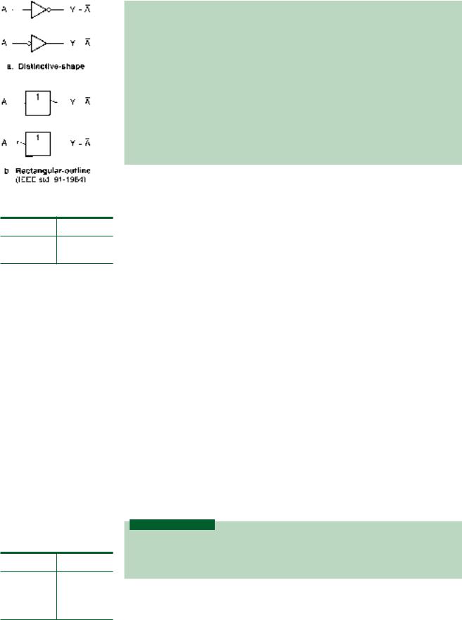
Table 2.1 NOT Function
Truth Table
A Y
0 1
1 0
FIGURE 2.1
Inverter Symbols
Table 2.2 2-input AND
Function Truth Table
A B Y
0 0 0
0 1 0
1 0 0
1 1 1
2.1 • Basic Logic Functions |
27 |
Distinctive-shape symbols Graphic symbols for logic circuits that show the function of each type of gate by a special shape.
IEEE/ANSI Standard 91-1984 A standard format for drawing logic circuit symbols as rectangles with logic functions shown by a standard notation inside the rectangle for each device.
Rectangular-outline symbols Rectangular logic gate symbols that conform to
IEEE/ANSI Standard 91-1984.
Qualifying symbol A symbol in IEEE/ANSI logic circuit notation, placed in the top center of a rectangular symbol, that shows the function of a logic gate. Some of the qualifying symbols include: 1 “buffer”; & “AND”; 1 “OR”
Buffer An amplifier that acts as a logic circuit. Its output can be inverting or noninverting.
NOT Function
The NOT function, the simplest logic function, has one input and one output. The input can be either HIGH or LOW (1 or 0), and the output is always the opposite logic level. We can show these values in a truth table, a list of all possible input values and the output resulting from each one. Table 2.1 shows a truth table for a NOT function, where A is the input variable and Y is the output.
The NOT function is represented algebraically by the Boolean expression:
Y A
This is pronounced “Y equals NOT A” or “Y equals A bar.” We can also say “Y is the complement of A.”
The circuit that produces the NOT function is called the NOT gate or, more usually, the inverter. Several possible symbols for the inverter, all performing the same logic function, are shown in Figure 2.1.
The symbols shown in Figure 2.1a are the standard distinctive-shape symbols for the inverter. The triangle represents an amplifier circuit, and the bubble (the small circle on the input or output) represents inversion. There are two symbols because sometimes it is convenient to show the inversion at the input and sometimes it is convenient to show it at the output.
Figure 2.1b shows the rectangular-outline inverter symbol specified by IEEE/ANSI Standard 91-1984. This standard is most useful for specifying the symbols for more complex digital devices. We will show the basic gates in both distinctive-shape and rectangu- lar-outline symbols, although most examples will use the distinctive-shape symbols.
The “1” in the top center of the IEEE symbol is a qualifying symbol, indicating the logic gate function. In this case, it shows that the circuit is a buffer, an amplifying circuit used as a digital logic element. The arrows at the input and output of the two IEEE symbols show inversion, like the bubbles in the distinctive-shape symbols.
AND Function
K E Y T E R M S
AND gate A logic circuit whose output is HIGH when all inputs (e.g., A AND B AND C) are HIGH.
Logical product AND function.
The AND function combines two or more input variables so that the output is HIGH only if all the inputs are HIGH. The truth table for a 2-input AND function is shown in Table 2.2.
28 C H A P T E R 2 • Logic Functions and Gates
Algebraically, this is written:
Y A B
FIGURE 2.2
2-Input AND Gate Symbols
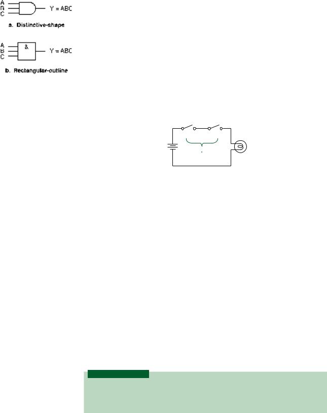
Pronounce this expression “Y equals A AND B.” The AND function is similar to multiplication in linear algebra and thus is sometimes called the logical product. The dot between variables may or may not be written, so it is equally correct to write Y AB. The logic circuit symbol for an AND gate is shown in Figure 2.2 in both distinctive-shape and IEEE/ANSI rectangular-outline form. The qualifying symbol in IEEE/ANSI notation is the ampersand (&).
We can also represent the AND function as a set of switches in series, as shown in Figure 2.3. The circuit consists of a voltage source, a lamp, and two series switches. The lamp turns on when switches A AND B are both closed. For any other condition of the switches, the lamp is off.
Table 2.3 3-input AND
Function Truth Table
A |
B |
C |
Y |
|
|
|
|
0 |
0 |
0 |
0 |
0 |
0 |
1 |
0 |
0 |
1 |
0 |
0 |
0 |
1 |
1 |
0 |
1 |
0 |
0 |
0 |
1 |
0 |
1 |
0 |
1 |
1 |
0 |
0 |
1 |
1 |
1 |
1 |
|
|
|
|
Table 2.4 |
2-input OR |
||
Function Truth Table |
|
||
|
|
|
|
A |
B |
|
Y |
|
|
|
|
0 |
0 |
|
0 |
0 |
1 |
|
1 |
1 |
0 |
|
1 |
1 |
1 |
|
1 |
|
|
|
|
|
A |
B |
|
Voltage |
|
Lamp |
|
source |
|
||
A |
B |
||
|
FIGURE 2.3
AND Function Represented by Switches
Table 2.3 shows the truth table for a 3-input AND function. Each of the three inputs can have two different values, which means the inputs can be combined in 23 8 different ways. In general, n binary (i.e., two-valued) variables can be combined in 2n ways.
Figure 2.4 shows the logic symbols for the device. The output is HIGH only when all inputs are HIGH.
FIGURE 2.4
3-Input AND Gate Symbols
OR Function
K E Y T E R M S
OR gate A logic circuit whose output is HIGH when at least one input (e.g., A OR B OR C) is HIGH.
Logical sum OR function.
The OR function combines two or more input variables in such a way as to make the output variable HIGH if at least one input is HIGH. Table 2.4 gives the truth table for the 2-in- put OR function.
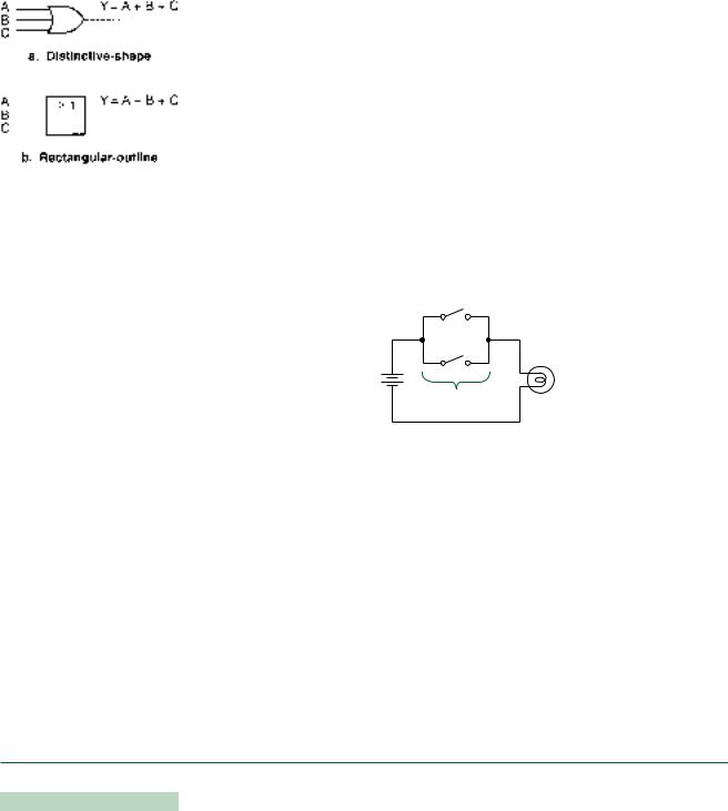
FIGURE 2.5
2-Input OR Gate Symbols
Table 2.5 |
3-input OR |
|
||
Function Truth Table |
|
|||
|
|
|
|
|
A |
B |
C |
|
Y |
|
|
|
|
|
0 |
0 |
0 |
|
0 |
0 |
0 |
1 |
|
1 |
0 |
1 |
0 |
|
1 |
0 |
1 |
1 |
|
1 |
1 |
0 |
0 |
|
1 |
1 |
0 |
1 |
|
1 |
1 |
1 |
0 |
|
1 |
1 |
1 |
1 |
|
1 |
|
|
|
|
|
2.1 • Basic Logic Functions |
29 |
The algebraic expression for the OR function is:
Y A B
which is pronounced “Y equals A OR B.” This is similar to the arithmetic addition function, but it is not the same. The last line of the truth table tells us that 1 1 1 (pronounced “1 OR 1 equals 1”), which is not what we would expect in standard arithmetic. The similarity to the addition function leads to the name logical sum. (This is different from the “arithmetic sum,” where, of course, 1 1 does not equal 1.)
Figure 2.5 shows the logic circuit symbols for an OR gate. The qualifying symbol for the OR function in IEEE/ANSI notation is “ 1,” which tells us that one or more inputs must be HIGH to make the output HIGH.
The OR function can be represented by a set of switches connected in parallel, as in Figure 2.6. The lamp is on when either switch A OR switch B is closed. (Note that the lamp is also on if both A and B are closed. This property distinguishes the OR function from the Exclusive OR function, which we will study later in this chapter.)
|
A |
|
|
B |
|
Voltage |
Lamp |
|
source |
||
|
||
|
A B |
FIGURE 2.6
OR Function Represented by Switches
Like AND gates, OR gates can have several inputs, such as the 3-input OR gates shown in Figure 2.7. Table 2.5 shows the truth table for this gate. Again, three inputs can be combined in eight different ways. The output is HIGH when at least one input is HIGH.
FIGURE 2.7
3-Input OR Gate Symbols
EXAMPLE 2.1
Application
State which logic function is most suitable for the following operations. Draw a set of switches to represent each function.
1.A manager and one other employee both need a key to open a safe.
2.A light comes on in a storeroom when either (or both) of two doors is open. (Assume the switch closes when the door opens.)
3.For safety, a punch press requires two-handed operation.
SOLUTION
1.Both keys are required, so this is an AND function. Figure 2.8a shows a switch representation of the function.