Digital design with CPLD applications and VHDL (R. Dueck, 2000)
.pdf210 C H A P T E R 5 • Combinational Logic Functions
Table 5.12 Exclusive
OR Truth Table
A |
B |
A B |
|
|
|
0 |
0 |
0 |
0 |
1 |
1 |
1 |
0 |
1 |
1 |
1 |
0 |
|
|
|
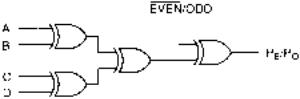
FIGURE 5.65
Even Parity Generation
FIGURE 5.66
Even Parity Checking
|
Figure 5.66 shows a parity checker for the parity generator in Figure 5.65. Data are re- |
|
ceived serially, but read in parallel. The parity bit is re-created from the received values of |
|
A and B, and then compared to the received value of P to give an error indication, P . If P |
|
and A B are the same, then P 0 and the transmission is correct. If P and A B are |
|
different, then P 1 and there has been an error in transmission. |
|
|
EXAMPLE 5.17 |
The following data and parity bits are transmitted four times: ABP 101. |
|
1. State the type of parity used. |
|
2. The transmission line over which the data are transmitted is particularly noisy and the |
|
data arrive differently each time as follows: |
|
a. ABP 101 |
|
b. ABP 100 |
|
c. ABP 111 |
|
d. ABP 110 |
|
Indicate the output P of the parity checker in Figure 5.66 for each case and state what |
|
the output means. |
Solution
1.The system is using EVEN parity.
2.The parity checker produces the following responses:
a.ABP 101
A B 1 0 1
P (A B ) P 1 1 0 Data received correctly.
b.ABP 100
A B 1 0 1
P (A B) P 1 0 1 Transmission error. (Parity bit incorrect.)
c.ABP 111

212 |
C H A P T E R 5 • Combinational Logic Functions |
|
|
|
|
|
|
Generator: |
|
|
|
|
|
|
Data: AB 11 |
Parity: P A B 1 |
1 1 |
|
|
|
|
|
|
|
|
|
|
|
Checker: |
|
|
|
|
|
|
Received data: AB 01 |
|
|
|
|
|
|
P (A B) P (0 1) 1 0 |
1 |
1 |
(Incorrect transmission) |
|
|
Parity generators and checkers can be expanded to any number of bits by using an XOR gate for each pair of bits and combining the gate outputs in further stages of 2-input XOR gates. The true form of the generated parity bit is PE, the EVEN parity bit. The complement form of the bit is PO, the ODD parity bit.
Table 5.13 shows the XOR truth table for 4 data bits and the ODD and EVEN parity bits. The EVEN parity bit PE is given by (A B) (C D). The ODD parity bit
Table 5.13 Even and Odd Parity Bits for 4-bit Data
A B C D |
A B C D |
PE |
PO |
||||
|
|
|
|
|
|
|
|
0 |
0 |
0 |
0 |
0 |
0 |
0 |
1 |
0 |
0 |
0 |
1 |
0 |
1 |
1 |
0 |
0 |
0 |
1 |
0 |
0 |
1 |
1 |
0 |
0 |
0 |
1 |
1 |
0 |
0 |
0 |
1 |
0 |
1 |
0 |
0 |
1 |
0 |
1 |
0 |
0 |
1 |
0 |
1 |
1 |
1 |
0 |
1 |
0 |
1 |
1 |
0 |
1 |
1 |
0 |
1 |
0 |
1 |
1 |
1 |
1 |
0 |
1 |
0 |
1 |
0 |
0 |
0 |
1 |
0 |
1 |
0 |
1 |
0 |
0 |
1 |
1 |
1 |
0 |
1 |
1 |
0 |
1 |
0 |
1 |
1 |
0 |
1 |
1 |
0 |
1 |
1 |
1 |
0 |
1 |
0 |
1 |
1 |
0 |
0 |
0 |
0 |
0 |
1 |
1 |
1 |
0 |
1 |
0 |
1 |
1 |
0 |
1 |
1 |
1 |
0 |
0 |
1 |
1 |
0 |
1 |
1 |
1 |
1 |
0 |
0 |
0 |
1 |
|
|
|
|
|
|
|
|
|
|
|
|
|
PO is given by PE (A B) |
(C |
D). For every line in Table 5.13, the bit com- |
|
bination ABCDPE has an even number of 1s and the group ABCDPO has an odd num- |
||
|
ber of 1s. |
|
|
|
|
||
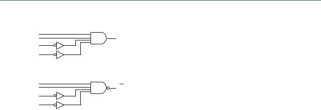
EXAMPLE 5.19 |
Use Table 5.13 to draw a 4-bit parity generator and a 4-bit parity checker that can generate |
||
|
and check either EVEN or ODD parity, depending on the state of one select input. |
||
FIGURE 5.68
Example 5.19
4-bit Parity Generator
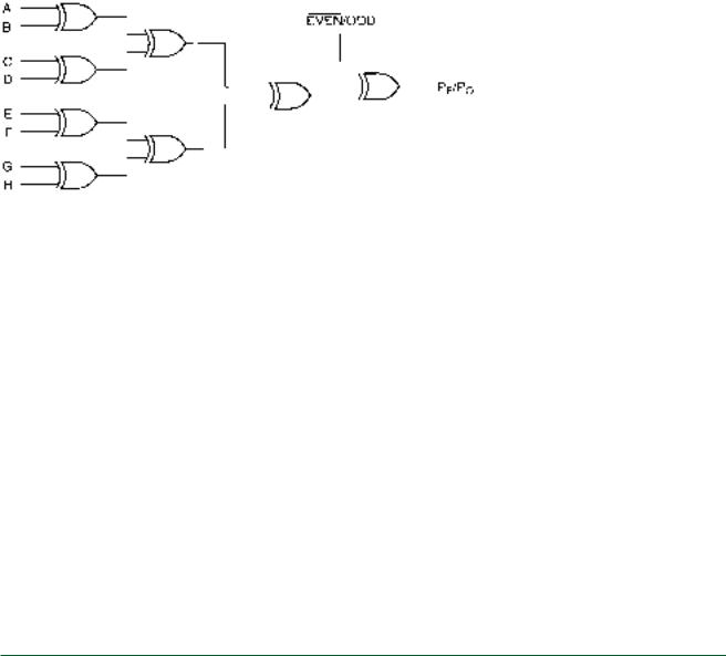
5.6 • Parity Generators and Checkers |
213 |
Solution Figure 5.68 shows the circuit for a 4-bit parity generator. The XOR gate at the output is configured as a programmable inverter to give PE or PO. When EVEN/ODD 0, the parity output is not inverted and the circuit generates PE. When EVEN/ODD 1, the
|
FIGURE 5.69 |
|
Example 5.19 |
|
4-bit Parity Checker |
|
|
EXAMPLE 5.20 |
Draw the circuit for an 8-bit EVEN/ODD parity generator. |
|
Solution An 8-bit parity generator is an expanded version of the 4-bit generator in the |
|
previous example. The circuit is shown in Figure 5.70. |
FIGURE 5.70
Example 5.20
8-bit Parity Generator
SECTION 5.6 REVIEW PROBLEM
5.6Data (including a parity bit) are detected at a receiver configured for checking ODD parity. Which of the following data do we know are incorrect? Could there be errors in the remaining data? Explain.
a.010010
b.011010
c.1110111
d.1010111
e.1000101