

Digital design with CPLD applications and VHDL (R. Dueck, 2000)
.pdf120 C H A P T E R 4 • Introduction to PLDs and MAX+PLUS II
N O T E
Although the examples in this book are created with the Altera UP-1 board in mind, they will easily adapt to other circuit boards carrying an Altera EPM7128S or other similar CPLD. One such board is available from Intectra Inc. For further information, contact Intectra at:
Intectra, Inc
2629 Terminal Blvd
Mountain View, CA 94043 U.S.A. Ph 650-967-8818 Fx 650-967-8836 intectra@best.com
www.intectra.com (Web site in Spanish only)
4.3 Graphic Design File
K E Y T E R M S
Graphic Design File (gdf) A PLD design file in which the digital design is entered as a schematic.
Project A set of MAX PLUS II files associated with a particular PLD design.
One way of entering PLD designs is to create a Graphic Design File. This type of file contains a representation of a digital circuit, such as in Figure 4.3, showing components and their interconnections, as well as specifying the inputs and output names of the circuit.
MAX PLUS II automatically generates a number of other files to keep track of the PLD programming information represented by the Graphic Design File. These files, taken together, represent a project in MAX PLUS II. All operations required to create a programming file for a CPLD are performed on a project, not a file. Thus, it is important during the design process to keep track of what the current project is. The MAX PLUS II toolbar, shown in Figure 4.6, makes this fairly easy.
Hierarchy |
Timing |
Project Save |
Project Save |
Search |
Display |
Simulator |
Programmer and Check |
and Simulate |
for Text |
Create |
Open |
Save |
Undo |
Compiler Timing |
Set Project |
Project |
Text |
New |
File |
File |
Last |
Analyzer |
to Current |
Save and |
Search |
File |
|
|
Action |
|
File |
Compile |
and |
|
|
|
|
|
|
|
Replace |
FIGURE 4.6
MAX PLUS II Toolbar
The toolbar has a number of buttons that pertain to the current project of a PLD design. The operations performed by these buttons can all be done through the regular menus of MAX PLUS II, but the toolbar offers a quick way to access many available functions. Not all buttons on the toolbar in Figure 4.6 are labeled, just the ones that you will find particularly convenient at this time. You can find out the function of any button by placing the cursor on the button and reading a description at the bottom of the window.
4.3 • Graphic Design File |
121 |
In particular, notice the buttons that create, open, and save files (standard Windows icons) and the button that sets the project to the current file. When creating a new file, make it standard practice to first Save the file, then Set Project to Current File. If you do this as a habit, you (and MAX PLUS II) will always know what the current project is. If you don’t, you will find that you are saving or compiling some other project and wondering why your last set of changes didn’t work.
Another good practice is to create a new Windows folder for each new design that you enter. Since MAX PLUS II creates many files in the design process, the folders would become unmanageable if designs were not kept in separate folders.
MAX PLUS II installs a folder for working with design files called max2work. The examples in this text will be created in a subfolder of max2work. If you are working in a situation where many people share a computer and you have access to a network drive of your own, you may wish to keep your working files in a max2work folder on the network drive. Avoid storing your working files on a local hard drive unless you are the only one with regular access to the computer. Examples in this book will not specify a drive letter, but will indicate drive:\max2work\folder.
Most of these examples are also available on the accompanying CD in the folder called Student Files. A special icon, shown in the margin, will indicate the example filename.
In the following sections, we will go through the process of creating a file in detail, using the majority vote circuit of Figure 4.3 as an example. The example assumes that MAX PLUS II is properly installed on your computer and running. For installation instructions, see the file SE_READ on the accompanying CD or the MAX PLUS II Installation section of MAX PLUS II Getting Started, available from Altera.
Entering Components
K E Y T E R M S
Primitives Basic functional blocks, such as logic gates, used in PLD design files.
Instance A single copy of a component in a PLD design file.
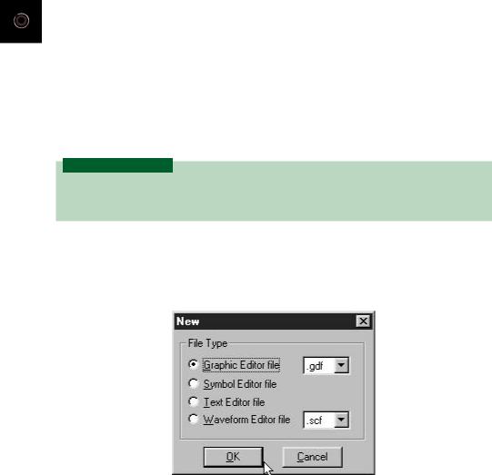
To create a Graphic Design File, click the New File icon on the tool bar or choose New on the MAX PLUS II File menu. The dialog box, shown in Figure 4.7 appears. Select Graphic Editor file and choose OK.
FIGURE 4.7
New Dialog Box
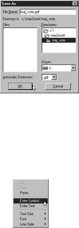
Maximize the window and click the Save icon or choose Save As or Save from the File menu. In the dialog box shown in Figure 4.8, save the file in a new folder (e.g., drive:\max2work\maj_vote\maj_vote.gdf) and choose OK. (If you have not created the new folder, just type the complete path name in the File Name box. MAX PLUS II will
122 C H A P T E R 4 • Introduction to PLDs and MAX+PLUS II
FIGURE 4.8
Save As Dialog Box
create a new folder.) Click the icon to Set Project to Current File or choose this action from the File, Project menu.
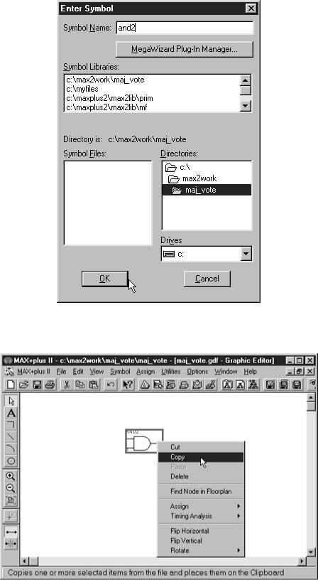
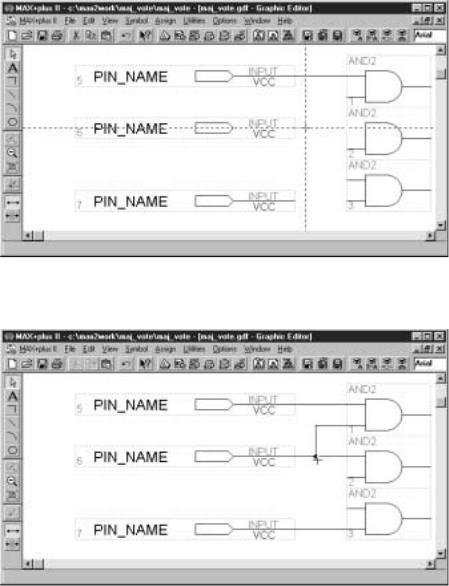
The first design step is to lay out and align the required components. We require three 2-input AND gates, a 3-input OR gate, three input pins, and one output pin. These basic components are referred to as primitives. Let us start by entering three copies of the AND gate primitive, called and2.
Click the left mouse button to place the cursor (a flashing square) somewhere in the middle of the active window. Right-click to get a pop-up menu, shown in Figure 4.9, and choose Enter Symbol. The dialog box in Figure 4.10 appears. Type and2 in the Symbol Name box and choose OK. A copy or instance of the and2 primitive appears in the active window.
FIGURE 4.9
Enter Symbol Pop-up Menu
You can repeat the above procedure to get two more instances of the and2 primitive, or you can use the Copy and Paste commands. These are the same icons and File commands as for other Windows programs. Highlight the and2 symbol by clicking it. Right-click the symbol to get the pop-up menu shown in Figure 4.11 and choose Copy. You can also click the Copy icon on the toolbar or use the Copy command in the File menu.
4.3 • Graphic Design File |
123 |
FIGURE 4.10
Enter Symbol Dialog Box
FIGURE 4.11
Copying a Component
124 C H A P T E R 4 • Introduction to PLDs and MAX+PLUS II
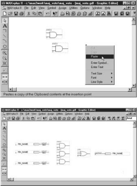
Paste an instance of the primitive by clicking to place the cursor, then right-clicking to bring up the menu shown in Figure 4.12. Choose Paste. The component will appear at the cursor location, marked in Figure 4.12 by the square at the top left corner of the pop-up menu.
Enter the remaining components by following the Enter Symbol procedure outlined above. The primitives are called or3, input, and output. When all components are entered we can align them, as in Figure 4.13 by highlighting, then dragging each one to a desired location.
FIGURE 4.12
Pasting a Component
FIGURE 4.13
Aligned Components
Connecting Components
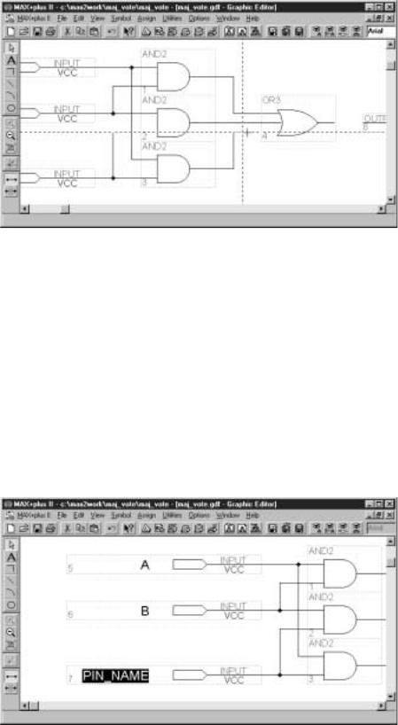
To connect components, click over one end of one component and drag a line to one end of a second component. When you drag the line, a horizontal and a vertical broken line mark the cursor position, as shown in Figure 4.14. These lines help you align connections properly.
4.3 • Graphic Design File |
125 |
FIGURE 4.14
Dragging a Line to Connect Components
FIGURE 4.15
Making a 90-degree Bend and a Connection
A line will automatically make a connection to a perpendicular line, as shown in Figure 4.15.
A line can have one 90-degree bend, as at the inputs of the AND gates. If a line requires two bends, such as shown at the AND outputs in Figure 4.16, you must draw two separate lines.
Assigning Pin Names
Before a design can be compiled, its inputs and outputs must be assigned names. We could also specify pin numbers, if we wished to make the design conform to a particular CPLD, but it is not necessary to do so at this stage. It may not even be desirable to assign pin numbers, since the design we enter can be used as a component or subdesign of a larger circuit. We may also wish MAX PLUS II to assign pins to make the best use of the CPLD’s internal resources. At any rate, we will leave this step out for now.
126 C H A P T E R 4 • Introduction to PLDs and MAX+PLUS II
FIGURE 4.16
Line with Two 90-degree Bends
Figure 4.17 shows the naming procedure. Pins A and B have already been assigned names. Highlight a pin by clicking on it. Right-click the highlighted pin and choose Edit Pin Name from the pop-up menu. You could also double-click the pin name to highlight it. Type in the new name.
If there are several pins that are spaced one above the other, you can highlight the top pin name, as described above, then highlight successive pin names by using the
Enter key.
FIGURE 4.17
Assigning Pin Names
4.4 • Compiling MAX+PLUS II Files |
127 |
4.4 Compiling MAX PLUS II Files
K E Y T E R M S
Programmer Object File (pof) Binary file used to program a PLD of the Altera MAX series.
SRAM Object File (sof) Binary file used to configure a PLD of the Altera FLEX series.
Volatile A device is volatile if it does not retain its stored information after the power to the device is removed.
Nonvolatile Able to retain stored information after power is removed.
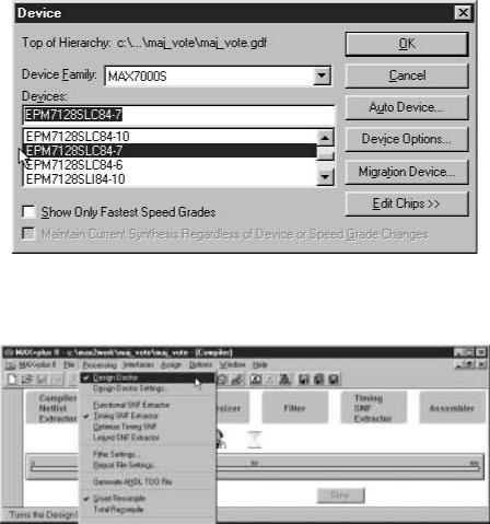
The MAX PLUS II compiler converts design entry information into binary files that can be used to program a PLD. Before compiling, we should assign a target device to the design.
From the Assign menu, shown in Figure 4.18, select Device. From the dialog box in Figure 4.19, select the target device. For the Altera UP-1 board, this would be either the EPM7128SLC84-7 (shown) or the FLEX10K20RC240-4. The device family for the EPM7128S device is MAX7000S.
FIGURE 4.18
Assign Menu
N O T E
To see the EPM7128SLC84-7 device, the box that says Show Only Fastest Speed Grades must be unchecked.
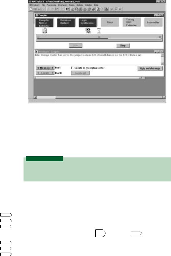
The compiler has a number of settings that can be chosen prior to the actual compile process. Figure 4.20 shows some of the settings that should be selected from the Processing menu of the Compiler window. You can open the Compiler window from the MAX PLUS II menu or by clicking the Compiler button on the toolbar at the top of the screen.
128 C H A P T E R 4 • Introduction to PLDs and MAX+PLUS II
FIGURE 4.19
Device Dialog Box
FIGURE 4.20
MAX PLUS II Compiler Settings
Design Doctor is a utility that checks for adherence to good design practice and will warn you of any bad design choices. (Design Doctor will not stop the design from compiling, but will suggest potential problems that could result from a particular design.) The Timing SNF Extractor creates a Simulation Netlist File, which is required to perform a timing simulation of the design. We will perform this step in later MAX PLUS II designs. (If you are not able to select the Timing SNF Extractor, then uncheck the Functional SNF Extractor option.) Smart Recompile allows the compiler to use previously compiled portions of the design to which no changes have been made. This allows the compiler to avoid having to compile the entire design each time a change is made to one part of the design.
To start the compile process, click Start in the Compiler window. While in progress, the window will look something like Figure 4.21. Message of three types may appear during the compile process. Info messages (green text) are for information only. Warning messages (blue text) tell you of potential, but nonfatal, problems with the design. Error messages (red text) inform you of design flaws that render the design unusable. A PLD can still be programmed if the compiler generates info or warning messages, but not if it generates an error.
Depending on the device chosen, the compiler generates either a Programmer Object File (pof) or SRAM Object File (sof). The pof is used to program a MAX-series PLD. The sof is used to configure a FLEX-series PLD. The difference is that the MAX de-
4.5 • Hierarchial Design |
129 |
FIGURE 4.21
MAX PLUS II Compiler Operation
vice is nonvolatile, that is, it retains its programming information after the power has been removed. The FLEX-series device is volatile, meaning that its programming information must be loaded each time the device powers up.
4.5 Hierarchical Design
K E Y T E R M S
Hierarchical design A PLD design that is ordered in layers or levels. The highest level of design contains components that are themselves complete designs. These components may, in turn, have lower level designs embedded within them.
A MAX PLUS II Graphical Design File can be used as part of a hierarchical design. That is, it can be represented as a component in a higher-level design. Figure 4.22 shows a gdf that is constructed as a hierarchical design. It contains two majority vote circuits whose
|
|
|
INPUT |
|
maj_vote |
||||||
|
|
|
|
|
|
|
|
|
|
|
|
A1 |
|
A |
|
|
|
|
|
|
|
||
INPUT |
|
|
|
|
|
|
|
||||
|
|
|
|
|
|
|
|
|
|
|
|
B1 |
|
|
B |
Y |
|
|
|
||||
C1 |
|
|
INPUT |
C |
|
|
AND2 |
||||
|
|
|
|
||||||||
|
|
|
|
||||||||
|
|
|
|
|
|
|
|
|
|
OUTPUT |
|
|
|
|
|
|
|
|
|
|
|
||
|
|
|
INPUT |
|
maj_vote |
|
|
|
|
Y |
|
|
|
|
|
|
|
|
|
||||
|
|
|
|
|
|
|
|
|
|||
|
|
|
|
|
|
|
|
|
|
|
|
A2 |
|
A |
|
|
|
|
|
|
|
||
INPUT |
|
|
|
|
|
|
|
||||
|
|
|
|
|
|
|
|
|
|
|
|
B2 |
|
|
B |
Y |
|
|
|
|
|
|
|
|
INPUT |
|
|
|
|
|
|
||||
C2 |
|
|
C |
|
|
|
|
|
|
|
|
|
|
|
|
|
|
|
|
|
|||
|
|
|
|
|
|
|
|
|
|||
|
|
|
|
|
|
|
|
|
|
|
|
FIGURE 4.22
Two-level Majority Vote Circuit (2votes.gdf)