

Digital design with CPLD applications and VHDL (R. Dueck, 2000)
.pdf160 |
C H A P T E R 5 |
• Combinational Logic Functions |
|
|
||
FIGURE 5.6 |
D2 |
|
|
|
||
|
|
|
||||
3-line-to-8-line Decoder with |
D1 |
|
|
|
||
|
|
|
||||
Enable |
|
D0 |
|
|
|
|
|
|
|
|
|
||
G
Y0
Y1
Y2
Y3
Y4
Y5
Y6
Y7
Figure 5.6 shows the circuit for a 3-line-to-8-line decoder, again with an active-LOW enable, G. In this case, the decoder outputs are active LOW. One and only one output is active for any given combination of D2D1D0. Table 5.2 shows the truth table for this decoder. Again if the enable line is HIGH, no output is active.
Table 5.2 Truth Table of a 3-to-8 Decoder with Enable
G |
D2 |
D1 |
D0 |
Y0 |
Y1 |
Y2 |
Y3 |
Y4 |
Y5 |
Y6 |
Y7 |
|
|
|
|
|
|
|
|
|
|
|
|
0 |
0 |
0 |
0 |
0 |
1 |
1 |
1 |
1 |
1 |
1 |
1 |
0 |
0 |
0 |
1 |
1 |
0 |
1 |
1 |
1 |
1 |
1 |
1 |
0 |
0 |
1 |
0 |
1 |
1 |
0 |
1 |
1 |
1 |
1 |
1 |
0 |
0 |
1 |
1 |
1 |
1 |
1 |
0 |
1 |
1 |
1 |
1 |
0 |
1 |
0 |
0 |
1 |
1 |
1 |
1 |
0 |
1 |
1 |
1 |
0 |
1 |
0 |
1 |
1 |
1 |
1 |
1 |
1 |
0 |
1 |
1 |
0 |
1 |
1 |
0 |
1 |
1 |
1 |
1 |
1 |
1 |
0 |
1 |
0 |
1 |
1 |
1 |
1 |
1 |
1 |
1 |
1 |
1 |
1 |
0 |
1 |
X |
X |
X |
1 |
1 |
1 |
1 |
1 |
1 |
1 |
1 |
|
|
|
|
|
|
|
|
|
|
|
|
EXAMPLE 5.3
Application
Figure 5.7 shows a partial Graphic Design File, created in MAX PLUS II, that shows how a 3-line-to-8-line decoder, such as the one shown in Figure 5.6, can be used in a microcomputer memory system as an address decoder. Each block labeled 8k_sram is a memory chip capable of holding 8192 (8K) bytes of data. Since there are eight such devices, the

|
|
|
|
|
|
|
|
|
|
|
|
|
|
5.1 • |
Decoders |
161 |
||||
|
|
|
|
|
|
|
ADDR[12..0] |
8k_sram |
|
dq0 |
ADDR[12..0] |
8k_sram |
dq4 |
|||||||
|
|
|
|
|
|
|
addr |
dq |
|
addr |
dq |
|||||||||
|
|
|
|
|
|
|
|
y0 |
|
|
|
|
|
y4 |
|
|
||||
|
|
|
|
|
|
|
|
g |
|
|
|
|
|
|
g |
|
|
|
||
|
|
|
|
|
|
|
|
|
|
|
|
|
|
|
|
|
|
|
||
|
|
|
|
|
|
|
|
|
|
|
|
|
|
|
|
|
|
|
||
|
|
|
|
|
|
|
ADDR[12..0] |
8k_sram |
|
dq1 |
ADDR[12..0] |
8k_sram |
dq5 |
|||||||
|
|
|
|
|
|
|
addr |
dq |
|
addr |
dq |
|||||||||
|
|
|
|
|
|
|
|
y1 |
|
|
|
|
|
y5 |
|
|
||||
|
|
|
|
|
|
|
|
g |
|
|
|
|
|
|
g |
|
|
|
||
|
|
|
|
|
|
|
|
|
|
|
|
|
|
|
|
|
|
|
||
|
|
|
|
|
|
|
|
|
|
|
|
|
|
|
|
|
|
|
|
|
|
|
INPUT |
|
|
|
|
y[0..7] |
|
|
|
|
|
|
|
|
|
|
|
|
|
ADDR[15..13] |
|
|
d[2..0] |
y[0..7] |
|
|
|
|
|
|
|
|
|
|
|
|
||||
|
INPUT |
|
|
|
|
|
|
|
|
|
|
|
|
|
|
|
||||
MEM_SELECT |
|
g |
|
|
|
8k_sram |
|
|
|
|
|
|
8k_sram |
|
|
|||||
|
|
|
ADDR[12..0] |
|
dq2 |
ADDR[12..0] |
dq6 |
|||||||||||||
|
|
|
|
|
|
|
|
|
|
|
|
|||||||||
|
|
|
|
|
|
|
addr |
dq |
|
addr |
dq |
|||||||||
|
|
|
|
|
|
|
|
y2 |
|
|
|
|
|
y6 |
|
|
||||
|
|
|
|
|
|
|
|
g |
|
|
|
|
|
|
g |
|
|
|
||
ADDR[12..0] |
INPUT |
ADDR[12..0] |
|
|
|
|
|
|
|
|
|
|
|
|
|
|||||
|
|
|
|
|
|
|
|
|
|
|
|
|
|
|
||||||
|
|
|
|
|
|
|
|
|
|
|
|
|
|
|
||||||
|
|
|
|
|
ADDR[12..0] |
8k_sram |
|
dq3 |
ADDR[12..0] |
8k_sram |
dq7 |
|||||||||
|
|
|
|
|
|
|
|
|||||||||||||
|
|
|
|
|
|
|
addr |
dq |
|
addr |
dq |
|||||||||
|
|
|
|
|
|
|
|
|
|
|
|
|
|
|
|
y7 |
|
|
|
|
|
|
|
|
|
|
|
|
y3 |
g |
|
|
|
|
|
|
g |
|
|
|
|
|
|
|
|
|
|
|
|
|
|
|
|
|
|
|
|
|
|
|
||
|
|
|
|
|
|
|
|
|
|
|
|
|
|
|
|
|
|
|
|
|
|
|
|
|
|
|
|
|
|
dq[0..7] |
|
OUTPUT |
|
|
dq[0..7] |
|
|
|
|||
|
|
|
|
|
|
|
|
|
|
|
|
|
|
|
|
|
|
|
||
FIGURE 5.7
Example 5.3
Address Decoder for a Memory System
whole system can hold 8 8192 65,536 (64K) bytes. (Although this amount of memory may seem small by the standards of a desktop computer, it may be typical of a small stand-alone computer system (called an embedded system or a microcontroller) that is used in control applications.)
Each 8K block is enabled by a LOW at its G input. Briefly explain the function of the decoder in the system.
Solution Since only one decoder output is LOW at any one time, the decoder allows only one memory block to be active at any one time. The active block is chosen by inputs ADDR15 ADDR14 ADDR13, which are connected to D2D1D0 on the decoder. The active memory block is the one connected to the y output whose subscript matches the binary value of these inputs. For example, when ADDR15 ADDR14 ADDR13 110, the block connected to y6 is active.
If the decoder is the same as the one in Figure 5.6, no outputs will be active, and therefore no memory block will be enabled, when G 1. (Note that the MAX PLUS II Graphic Editor cannot represent an input or output with an inversion bar. Some conventions would represent an active-LOW terminal with an “n” prefix, indicating “NOT” (e.g., nG). This is a matter of personal choice, but without such an indication it is not possible to tell the active level of an input or output from the MAX PLUS II Graphic Design File.)
The decoders in Figure 5.6 and 5.7 have identical functions, but the symbol in Figure 5.7 shows the D inputs and Y outputs as multibit vectors or busses. Figure 5.7 also shows how the individual signals in a bus can be connected to separate parts of the circuit in a MAX PLUS II Graphic Design File.
To make the connections, draw and label a line extending from each terminal. To label a line, highlight the line by clicking on it with the left mouse button, then right-click. Select Enter Node/Bus Name from the pop-up menu and enter the text. Lines that have the same names are automatically connected by their text references. If a line is a multiple line,
162 C H A P T E R 5 • Combinational Logic Functions
it must have signal designators in brackets (e.g., y[0..7]). Individual signals from a bus must be numbered in a way that corresponds to the multiple-bit line (e.g., y0, y1, y2, and so on).
SECTION 5.1B REVIEW PROBLEM
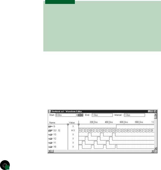
FIGURE 5.8
Simulation Waveforms for a 2- to-4 Decoder with Enable
2to4dcdr.gdf
2to4dcdr.scf
5.2How many inputs are required for a binary decoder with 16 outputs? How many inputs are required for a decoder with 32 outputs?
Simulation of a 2-Line-to-4-Line Decoder
K E Y T E R M S
Timing diagram A diagram showing how two or more digital waveforms in a system relate to each other over time.
Simulation The verification, using timing diagrams, of the logic of a digital design before programming it into a PLD.
Stimulus waveforms A set of user-defined input waveforms in a simulator file
designed to imitate input conditions of a digital circuit.
Response waveforms A set of output waveforms generated by a simulator for a particular digital design in response to a set of stimulus waveforms.
Propagation delay Time difference between a change on a digital circuit input and a change on an output in response to the input change.
An important part of the CPLD design process is simulation of the design. A simulation tool allows us to see whether the output responses to a set of circuit inputs are what we expected in our initial design idea. The simulator works by creating a timing diagram. We specify a set of input (stimulus) waveforms. The simulator looks at the relationship between inputs and outputs, as defined by the design file, and generates a set of response outputs.
Figure 5.8 shows a set of simulation waveforms created for the 2-line-to-4-line decoder in Figure 5.4. The inputs D1 and D0 are combined as a single 2-bit value, to which an increasing binary count is applied as a stimulus. The decoder output waveforms are observed individually to determine the decoder’s response. Once we have entered the design in the MAX PLUS II Graphic Editor and compiled it, we can create the waveforms as follows.
dialog box, select Waveform EdiFile menu, choose Save As, then enter
5.1 • Decoders |
163 |
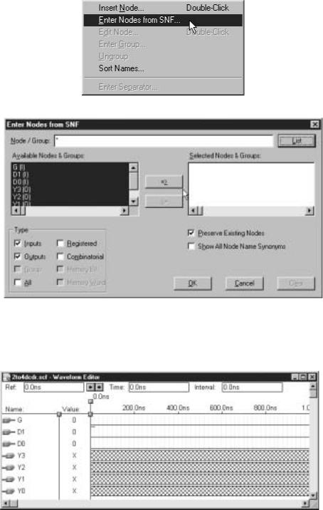
We specify the inputs and outputs we want to view by selecting Enter Nodes from SNF on the Node menu, shown in Figure 5.9. In the dialog box that pops up (Figure 5.10), there are two boxes labelled Available Nodes & Groups and Selected Nodes & Groups, with an arrow ( ) pointing from one to the other. Select the List button to show the “available” signals and click the arrow to transfer them all to the “selected” box. Click OK to close the box.
FIGURE 5.9
Node Menu
FIGURE 5.10
Selecting Nodes for Waveform
Editor
Figure 5.11 shows the simulation waveforms in their uninitialized (default) states. Inputs and outputs are shown by symbols in front of the signal names. Inputs are at logic 0 and outputs are indicated as X or unknown values.
FIGURE 5.11
Default Values of Simulation Waveforms
164 C H A P T E R 5 • Combinational Logic Functions
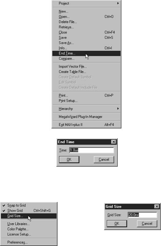
We now set the timing length of the simulation. The default value is 1 s, written 1.0us. For this example, we will leave the end time at the default value. However, if we want to change it, we select End Time (File menu, Figure 5.12) and enter the new time for the end of simulation in the dialog box of Figure 5.13. Click OK.
FIGURE 5.12
Setting the End Time of a
Simulation (File Menu)
FIGURE 5.13
End Time Dialog Box
FIGURE 5.14
Setting Simulation Grid
Size (Options Menu)
The End Time dialog sets the end of the simulation. We should also set the Grid Size, which determines the size of the smallest time division in the simulation. To do so, select Grid Size from the Options menu, shown in Figure 5.14. In the dialog box of Figure 5.15, enter the value 20ns and click OK. (We will use this value for many of our simulations
FIGURE 5.15
Grid Size Dialog Box
5.1 • Decoders |
165 |
because it corresponds to one half period of the oscillator on the Altera UP-1 board. In the simulator, one full period requires two grid spaces.)
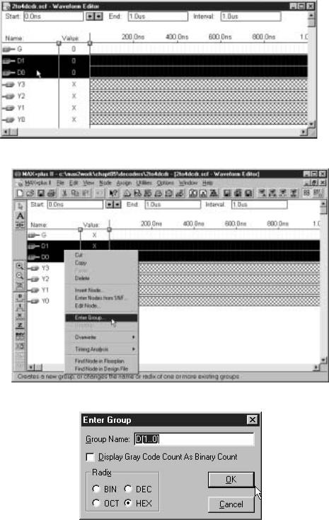
When we created the simulation file, the D inputs were entered as separate waveforms. We can join these waveforms to make a Group. Highlight both D1 and D0 by clicking on one name and dragging the mouse to the next name, as in Figure 5.16. From the Node menu or the pop-up menu in Figure 5.17, select Enter Group. The dialog box shown in Figure 5.18 appears, containing the most likely name derived from the highlighted group. Either type a new group name or accept the original name by clicking OK.
FIGURE 5.16
Highlighting a Group
FIGURE 5.17
Pop-up Menu (Enter Group)
FIGURE 5.18
Enter Group Dialog Box
166 C H A P T E R 5 • Combinational Logic Functions
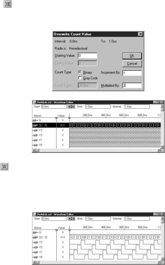
Overwrite Count
Button
As a decoder stimulus, we will define an increasing binary count on the D inputs. Highlight the input group by clicking in the Value column. Use the Overwrite Count toolbar button to create an increasing binary count on the group, D[1..0]. Fill in the dialog box as shown in Figure 5.19 and click OK. The count is increased every 40 ns (2 20 ns), as shown in Figure 5.20.
FIGURE 5.19
Overwrite Count Value Dialog
Box
FIGURE 5.20
Group Input with Binary Count
Fit in Window
Button
FIGURE 5.21
Decoder Simulation with Enable Always Active
Save the file. From the MAX PLUS II menu, bring the Simulator to the front and click Start. When the simulation is finished (almost immediately), click Open SCF and maximize the window. From the View menu, select Fit in Window or select the toolbar button for this function.
The simulator output, shown in Figure 5.21, shows the result of a repeating binary count at the decoder input when the outputs are always enabled. The outputs activate in a repeating sequence, from Y0 to Y3.
You will notice that the D inputs change exactly on the grid lines, but the Y outputs change slightly after. This is due to propagation delay, defined as the time between an
Overwrite with
HIGH Button
decode1.vhd
decode2.vhd
5.1 • Decoders |
167 |
input change and the time an output changes in response to that input. In the EPM7128SLC84-7 CPLD, for which this simulation is created, propagation delay is about 7 nanoseconds. (The MAX PLUS II simulator accounts for the propagation delay in different CPLDs.) Later simulations in this chapter will not necessarily show the delay, as the timing chosen may be very long compared to delay times.
To see the result of the enable input, highlight the G waveform from approximately 500 ns to 1 s by dragging the mouse along this part of the waveform. Overwrite the highlighted part by clicking the Overwrite with HIGH button. When we run the simulation again, we get the waveforms shown in Figure 5.8.
VHDL Binary Decoder
K E Y T E R M S
Selected signal assignment statement A concurrent signal assignment in VHDL in which a value is assigned to a signal, depending on the alternative values of another signal or variable.
Conditional signal assignment statement A concurrent VHDL construct that assigns a value to a signal, depending on a sequence of conditions being true or false.
In Chapter 4, we saw an example of how we can use VHDL to define the function of a 2-line-to-4-line decoder. For reference the description is replicated below, with the difference that the input and output ports are defined as BIT rather than STD_LOGIC types. (This is sufficient for a combinational circuit like a decoder, as the only I/O (input/output) values required are ‘0’ and ‘1’. If we use BIT types, we do not require a reference to the IEEE library, as we do to define STD_LOGIC types.)
ENTITY decode1 IS
PORT(
d1, d0 : IN BIT;
y0, y1, y2, y3 : OUT BIT); END decode1;
ARCHITECTURE |
decoder1 OF decode1 IS |
|||
BEGIN |
|
|
|
|
y0 |
<= (not |
d1) |
and (not d0); |
|
y1 |
<= (not |
d1) |
and ( |
d0); |
y2 |
<= ( |
d1) |
and (not |
d0); |
y3 |
<= ( |
d1) |
and ( |
d0); |
END decoder1;
The above formulation has no enable input. If we wish to include the enable function, we must modify the entity declaration to include that input and change the signal assignment statements, as well. The new VHDL code is as follows.
ENTITY decode2 IS
PORT(
d1, d0, g : IN BIT; y0, y1, y2, y3 : OUT BIT);
END decode2;
ARCHITECTURE decoder2 OF decode2 IS
BEGIN |
|
|
|
|
|
|
y0 |
<= |
(not d1) |
and (not d0) |
and (not g); |
||
y1 |
<= |
(not d1) |
and ( |
d0) |
and (not g); |
|
y2 |
<= |
( |
d1) |
and (not d0) |
and (not g); |
|
y3 |
<= |
( |
d1) |
and ( |
d0) |
and (not g); |
END decoder2;

168 C H A P T E R 5 • Combinational Logic Functions
In addition to coding the Boolean expressions directly, we can use two types of concurrent signal assignments to create decoder circuits: the selected signal assignment statement and the conditional signal assignment statement. Both the Altera VHDL manual and the Help menu in MAX PLUS II have a section on “Golden Rules” for VHDL. The VHDL Golden Rules suggest that you should use a selected signal assignment rather than a conditional signal assignment, if possible. This is because, in certain cases, the selected signal assignment uses the internal circuitry of the CPLD more efficiently.
The selected signal assignment has the form:
label: WITH __expression SELECT
__signal <=__expression WHEN __constant_value, __expression WHEN __constant_value, __expression WHEN __constant_value, __expression WHEN __constant_value;
The signal indicated in the second line of the statement template is assigned one of several expressions, depending on the constant value of the expression in the first line. The label is optional. Examine the selected signal statement below:
circuit: |
WITH mode SELECT |
|
y |
<= q |
WHEN “00” |
|
not q |
WHEN “01”, |
|
p |
WHEN “11”, |
|
‘1’ |
WHEN others; |
Signal y is assigned one of three values, p, q, or not q, depending on the status of a two-bit variable called mode. Note that the value of y for the case when mode “10” is not explicitly stated. This is covered by the last clause (WHEN others), which defines a default value for signal y of logic 1.
The following VHDL code implements a 2-line-to-4-line decoder using a selected signal assignment statement.
decode3.vhd
PORT( |
|
|
|
d |
: IN |
STD_LOGIC_VECTOR (1 |
downto 0); |
y |
: OUT |
STD_LOGIC_VECTOR (3 |
downto 0)); |
END decode3;
ARCHITECTURE decoder OF decode3 IS
BEGIN
WITH d SELECT
y <= “0001” WHEN “00”, “0010” WHEN “01”, “0100” WHEN “10”, “1000” WHEN “11”, “0000” WHEN others;
END decoder;
The selected signal assignment statement evaluates input d. For every possible combination of the 2-bit input vector, d, a particular value is assigned to the 4-bit vector, y. (For
example, for the case d1d0 10 ( 210), the output y2 is HIGH: y3y2y1y0 0100.)
The default case (“WHEN others”) is required because of the multivalued logic type STD_LOGIC_VECTOR. Since a STD_LOGIC_VECTOR can have values other than ‘0’ and ‘1’, the values listed for d don’t cover all possible cases. The default output (which will never occur if we only use ‘0’ and ‘1’ inputs) is chosen such that no output is active in the

5.1 • Decoders |
169 |
default case. The default case would not be required if we chose to use BIT_VECTOR, rather than STD_LOGIC_VECTOR, since the listed combinations of d cover all possible combinations of a BIT_VECTOR. However, it is a good practice to include the default case, in order to account for all possible contingencies.
In order to include an enable input (g) in a decoder, we can increase the input vector size to include the g input, as shown in the following code.
|
decode3a.vhd |
|
_1164.ALL; |
|
|
||
|
|
||
|
ENTITY decode3a IS |
|
|
|
PORT( |
|
|
|
d |
: IN |
STD_LOGIC_VECTOR (1 downto 0); |
|
g |
: IN |
STD_LOGIC; |
|
y |
: OUT |
STD_LOGIC_VECTOR (3 downto 0)); |
END decode3a;
ARCHITECTURE decoder OF decode3a IS
SIGNAL inputs : STD_LOGIC_VECTOR (2 downto 0);
BEGIN |
|
|
inputs(2) |
|
<= g; |
inputs(1 downto 0) |
<= d; |
|
WITH inputs SELECT |
|
|
y <= |
“0001” WHEN “000”, |
|
|
“0010” WHEN “001”, |
|
|
“0100” WHEN “010”, |
|
|
“1000” WHEN “011”, |
|
|
“0000” WHEN others; |
|
END decoder; |
|
|
To include g and d in a single vector, we create a signal called inputs, a vector with three elements in the sequence g, d(1), d(0). When assigning the d to the last two elements of inputs, we must be explicit about which elements of inputs we want to use. Since d only contains two elements and we are assigning them to two elements of inputs, we don’t need to list the elements of d explicitly.
We can use a selected signal assignment statement to evaluate all inputs, including g , and assign outputs accordingly. When g ‘0’, the decoder outputs are assigned the same as they were in the example without the enable input. The cases where g ‘1’ are covered by the others clause. In this default case, all decoder outputs are LOW (inactive).
Another way to include an enable input is to use a conditional signal assignment statement, which makes an assignment based on a Boolean expression. This template for the conditional signal assignment statement is:
__signal <= __expression WHEN __boolean_expression ELSE
__expression WHEN __boolean_expression ELSE
__expression;
The first Boolean expression in the statement is evaluated. If it is true, the corresponding expression is assigned to the signal. If false, the next Boolean expression is evaluated, and so on until a true Boolean expression is found. If none are true, the signal is assigned a default expression, listed last in the statement.
The VHDL code below implements the decoder with an active-LOW enable. If g is LOW, one decoder output activates, depending on the value of d. Note that the d inputs are defined as type INTEGER, rather than BIT_VECTOR or STD_LOGIC_VECTOR. In this situation, we don’t need to specify the number of inputs; the compiler automatically defines the required inputs d1 and d0 when fitting the design to the selected CPLD. Also, since d is of type INTEGER, we write its value in the selected signal assignment statement directly, without quotes.