240 |
C H A P T E R 6 • Digital Arithmetic and Arithmetic Circuits |
FIGURE 6.2
Half Adder Circuit
FIGURE 6.3
Full Adder
Table 6.7 Full Adder Truth
Table
A |
B |
CIN |
COUT |
|
0 |
0 |
0 |
0 |
0 |
0 |
0 |
1 |
0 |
1 |
0 |
1 |
0 |
0 |
1 |
0 |
1 |
1 |
1 |
0 |
1 |
0 |
0 |
0 |
1 |
1 |
0 |
1 |
1 |
0 |
1 |
1 |
0 |
1 |
0 |
1 |
1 |
1 |
1 |
1 |
|
|
|
|
|
The corresponding logic circuit is shown in Figure 6.2.
The half adder circuit cannot account for an input carry, that is, a carry from a lowerorder 1-bit addition. A full adder, shown in Figure 6.3, can add two 1-bit numbers and accept a carry bit from a previous adder stage. Operation of the full adder is based on the following sums:
0 0 0 00
0 0 1 01
0 1 1 10
1 1 1 11
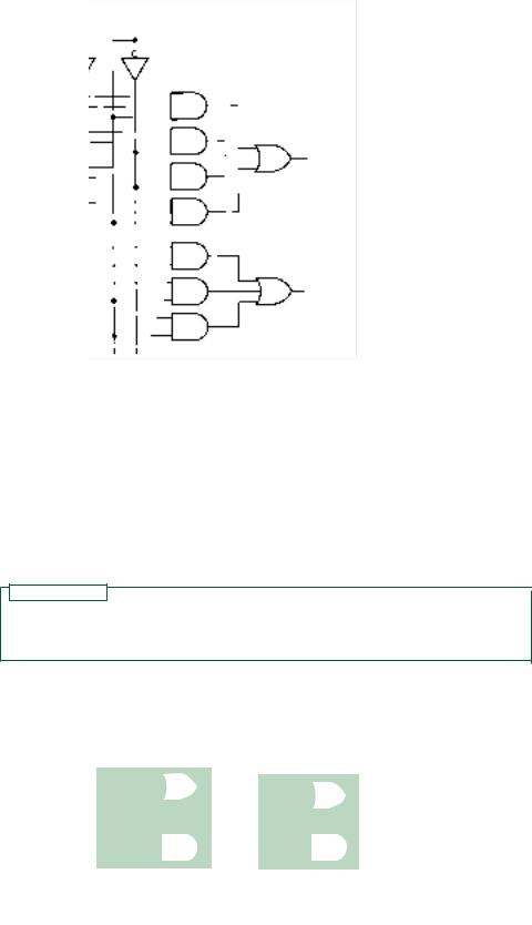
Designating the left side of the above equalities as circuit inputs A, B, and CIN and the right side as outputs COUT and , we can make the truth table in Table 6.7. (The second and third of the above sums each account for three lines in the full adder truth table.)
The unsimplified Boolean expressions for the outputs are:
COUT A B CIN A B CIN A B CIN A B CIN
A B CIN A B CIN A B CIN A B CIN
There are a couple of ways to simplify these expressions.
Karnaugh Map Method
Since we have expressions for and COUT in sum-of-products form, let us try to use the Karnaugh maps in Figure 6.4 to simplify them. The expression for doesn’t reduce at all.
The simplified expression for COUT is:
COUT A B A CIN B CIN
FIGURE 6.4
K-Maps for a Full Adder
The corresponding logic circuits for and COUT, shown in Figure 6.5, don’t give us much of a simplification.
Boolean Algebra Method
The simplest circuit for COUT and involves the Exclusive OR function, which we cannot derive from K-map groupings. This can be shown by Boolean algebra, as follows:
COUT A B CIN A B CIN A B CIN A B CIN
(A B A B)CIN A B (CIN CIN)
(A B) CIN A B
6.6 • Binary Adders and Subtractors |
241 |
FIGURE 6.5
Full Adder from K-Map Simplification
(A B AB) CIN (A B A B) CIN
(A B) CIN (A B) CIN |
Let x A B |
x CIN x CIN |
|
x CIN |
|
(A B) CIN |
|
The simplified expressions are as follows: |
|
N O T E
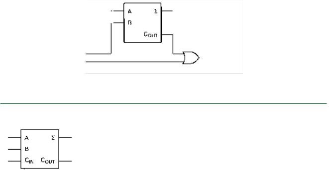
COUT (A B) CIN A B
(A B) CIN
Figure 6.6 shows the logic circuit derived from these equations. If you refer back to the half adder circuit in Figure 6.2, you will see that the full adder can be constructed from two half adders and an OR gate, as shown in Figure 6.7.
FIGURE 6.6
Full Adder from Logic Gates
242 |
C H A P T E R 6 • Digital Arithmetic and Arithmetic Circuits |
|
|
Half Adder |
Half Adder |
FIGURE 6.7
Full Adder From Two Half Adders
EXAMPLE 6.18
FIGURE 6.8
Example 6.18
Full Adder
Evaluate the Boolean expression for and COUT of the full adder in Figure 6.8 for the following input values. What is the binary value of the outputs in each case?
a.A 0, B 0, CIN 1
b.A 1, B 0, CIN 0
c.A 1, B 0, CIN 1
d.A 1, B 1, CIN 0
SOLUTION The output of a full adder for any set of inputs is simply given by COUT A B CIN. For each of the stated sets of inputs:
a.COUT A B CIN 0 0 1 01
b.COUT A B CIN 1 0 0 01
c.COUT A B CIN 1 0 1 10
d.COUT A B CIN 1 1 0 10
We can verify each of these sums algebraically by plugging the specified inputs into the full adder Boolean equations:
COUT (A B) CIN A B
(A B) CIN
a.COUT (0 0) 1 0 0
0 1 0
0 0 0
(0 0) 1 |
|
0 1 1 |
(Binary equivalent: COUT 01) |
b.COUT (1 0) 0 1 0
1 0 0
0 0 0
(1 0) 0 |
|
1 0 1 |
(Binary equivalent: COUT 01) |
c.COUT (1 0) 1 1 0
1 1 0
1 0 1
(1 0) 1
1 1 0 (Binary equivalent: COUT 10)
|
|
6.6 • Binary Adders and Subtractors |
243 |
|
d. COUT (1 1) 0 1 1 |
|
|
0 0 1 |
|
|
|
0 1 1 |
|
|
|
(1 1) 0 |
|
|
|
0 0 0 |
(Binary equivalent: COUT 10) |
|
|
In each case, the binary equivalent is the same as the number of HIGH inputs, regard- |
|
less of which inputs they are. |
|
|
|
EXAMPLE 6.19 |
Combine a half adder and a full adder to make a circuit that will add two 2-bit numbers. |
|
Check that the circuit will work by adding the following numbers and writing the binary |
|
equivalents of the inputs and outputs: |
|
a. A2 A1 01, B2 B1 01 b. A2 A1 11, B2 B1 10
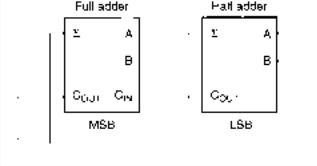
SOLUTION The 2-bit adder is shown in Figure 6.9. The half adder combines A1 and B1; A2, B2, and C1 are added in the full adder. The carry output, C1, of the half adder is connected to the carry input of the full adder. (A half adder can be used only in the LSB of a multiple-bit addition.)
FIGURE 6.9
Example 6.19
2-Bit Adder
Sums: |
|
|
|
|
a. 01 |
01 010 |
|
|
|
|
|
A1 1, B1 1 |
C1 1, 1 0 |
|
|
|
|
|
|
|
|
|
|
|
|
|
|
|
|
|
|
|
|
|
A2 0, B2 0, C1 1 |
C2 0, 2 1 |
|
|
(Binary equivalent: A2 A1 B2 B1 C2 2 1 010) |
|
b. 11 10 101 |
|
|
|
|
A1 1, B1 0 |
C1 0, 1 1 |
|
|
|
|
|
|
|
|
|
|
|
|
|
|
|
|
|
|
|
A2 1, B2 1, C1 0 |
C2 1, 2 0 |
|
|
(Binary equivalent: A2 A1 |
B2 B1 C2 2 1 |
101) |
|
|
|
|
|
|
|
6.6 • Binary Adders and Subtractors |
245 |
b.1111 0001 10000
(1510 110 1610)
A1 1, B1 1, C0 0; C1 1, 1 0 A2 1, B2 0, C1 1; C2 1, 2 0 A3 1, B3 0, C2 1; C3 1, 3 0 A4 1, B4 0, C3 1; C4 1, 4 0
(Binary equivalent: C4 4 3 2 1 10000)
The internal carries in the parallel binary adder in Figure 6.10 are achieved by a system called ripple carry. The carry output of one full adder cascades directly to the carry input of the next. Every time a carry bit changes, it “ripples” through some or all of the following stages. A sum is not complete until the carry from another stage has arrived. The equivalent circuit of a 4-bit ripple carry is shown in Figure 6.11.
|
A4 B4 |
A |
B4 |
|
A3B3 |
4 |
|
|
A3 B3 |
|
|
|
A2B2 |
|
C4 |
|
A2 B2 |
|
|
A1B1 |
|
|
|
A1 B1 |
|
|
|
C3 |
|
|
|
C2 |
|
|
C0 |
C1 |
|
|
FIGURE 6.11
4-bit Ripple Carry Chain
A potential problem with this design is that the adder circuitry does not switch instantaneously. A carry propagating through a ripple adder adds delays to the summation time and, more importantly, can introduce unwanted intermediate states.
Examine the sum (1111 0001 10000). For a parallel adder having a ripple carry, the output goes through the following series of changes as the carry bit propagates through the circuit:
C4 4 3 2 1 01111
01110
01100
01000
10000
If the output of the full adder is being used to drive another circuit, these unwanted intermediate states may cause erroneous operation of the load circuit.
Fast Carry
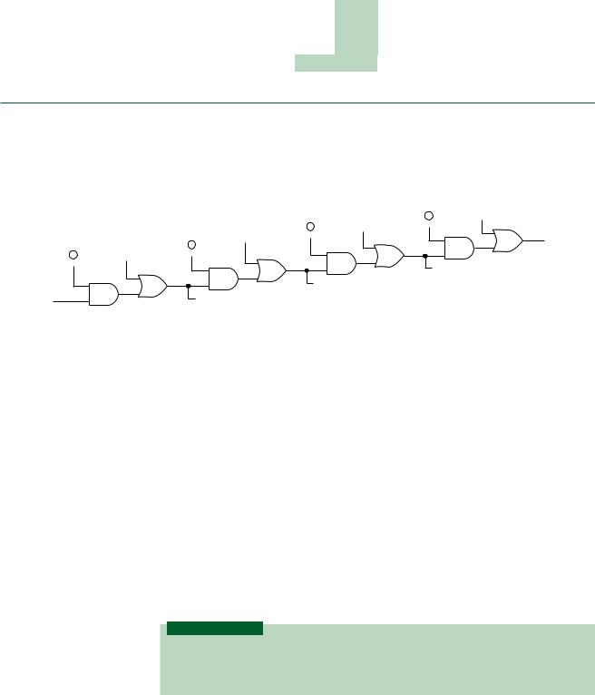
K E Y T E R M
Fast carry (or look-ahead carry) A gate network that generates a carry bit directly from all incoming operand bits, independent of the operation of each full adder stage.
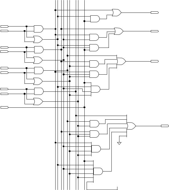
An alternative carry circuit is called fast carry or look-ahead carry. The idea behind fast carry is that the circuit will examine all the A and B bits simultaneously and produce an output carry that uses fewer levels of gating than a ripple carry circuit. Also, since there is
246 |
C H A P T E R 6 • Digital Arithmetic and Arithmetic Circuits |
a1
b1
a2
b2
a3
b3
a4
b4
c0
INPUT
INPUT
INPUT
INPUT
INPUT
INPUT
INPUT
INPUT
INPUT
|
OR2 |
|
|
AND2 |
c1 |
OUTPUT |
c1 |
|
|
|
|
|
AND2 |
OR3 |
|
|
|
|
|
AND2 |
c2 |
OUTPUT |
c2 |
|
|
|
|
|
OR2 |
|
|
|
AND3 |
|
|
|
AND2 |
|
|
|
OR2 |
OR4 |
|
|
|
|
|
AND2 |
c3 |
OUTPUT |
c3 |
|
|
|
AND2 |
|
|
|
AND3 |
|
|
|
OR2
AND4
AND2
OR2
OR6 |
|
|
AND2 |
|
|
c4 |
OUTPUT |
c4 |
|
|
AND3 |
|
|
AND4 |
|
|
GND |
|
|
AND6 |
|
|
VCC
FIGURE 6.12
4-bit Fast Carry Circuit
a carry bit gate network for each internal stage, the propagation delay is the same for each full adder, regardless of the input operands.
The algebraic relation between operand bits and fast carry output is presented below, without proof. It can be developed from the fast carry circuit of Figure 6.12 by tracing the logic of the gates in the circuit.
C4 A4 B4 A3 B3 (A4 B4) A2 B2 (A4 B4)(A3 B3)
A1 B1 (A4 B4)(A3 B3)(A2 B2)
C0 (A4 B4)(A3 B3)(A2 B2)(A1 B1)

6.6 • Binary Adders and Subtractors |
247 |
We can make some intuitive sense of the above expression by examining it a term at a time. The first term says if the MSBs of both operands are 1, there will be a carry (e.g., 1000 1000 10000; carry generated).
The second term says if both second bits are 1 AND at least one MSB is 1, there will be a carry (e.g., 0100 1100 10000, or 1100 1100 11000; carry generated in either case). This pattern can be followed logically through all the terms.
The internal carry bits are generated by similar circuits that drive the carry input of each full adder stage in the parallel adder. In general, we can generate each internal carry by expanding the following expression:
Cn AnBn Cn 1 (An Bn)
The algebraic expressions for the remaining carry bits are:
C1 A1B1 C0 (A1 B1)
C2 A2B2 A1 B1 (A2 B2) C0 (A2 B2)(A1 B1)
C3 A3B3 A2 B2 (A3 B3) A1 B1 (A3 B3)(A2 B2)C0 (A3 B3)(A2 B2)(A1 B1)
SECTION 6.6A REVIEW PROBLEM
6.9Refer to the logic diagrams for the ripple carry and fast carry circuits (Figures 6.11 and 6.12). How many gates must a carry bit propagate through in each device if the effect of the carry input ripples through to the 4 bit? (See Figure 6.32 on page 273 and Figure 6.33 on page 273.)
Using VHDL Components to Implement a Parallel Adder
K E Y T E R M S
Hierarchy A group of design entities associated in a series of levels or layers in which complete designs form portions of another, more general design entity. The more general design is considered to be the higher level of the hierarchy.
Component A complete VHDL design entity that can be used as a part of a higher-level file in a hierarchical design.
Port An input or output of a VHDL design entity or component.
Component declaration statement A statement that defines the input and output port names of a component used in a VHDL design entity.
Instantiate To use an instance of a component.
Component instantiation statement A statement that maps port names of a VHDL component to the port names, internal signals, or variables of a higher-level VHDL design entity.
VHDL designs can be created using a hierarchy of design entities. Certain functions, such as full adders, decoders, and so on, can be created once and used in many designs or multiple times in a single design.
We can create a parallel adder in VHDL by using multiple instances of a full adder component in the top-level file of a VHDL design hierarchy. Figure 6.13 shows a graphical illustration of this concept. Each full adder shown is an instance of a component written in VHDL, as shown in the following.
248 |
C H A P T E R 6 • Digital Arithmetic and Arithmetic Circuits |
FIGURE 6.13
4-bit Parallel Adder with Ripple Carry
ENTITY full_add IS
PORT (
a, b, c_in : IN BIT; c_out, sum : OUT BIT);
END full_add;
ARCHITECTURE adder OF full_add IS BEGIN
c_out ((a xor b) and c_in) or (a and b) ; sum (a xor b) xor c_in;
END adder;
|
|
|
|
|
FULL_ADD |
|
|
a1 |
|
INPUT |
a |
c_out |
|
OUTPUT |
|
INPUT |
|
OUTPUT |
b1 |
|
b |
sum |
|
|
INPUT |
|
|
c0 |
|
c_in |
|
|
|
|
|
|
|
|
|
|
|
|
|
|
|
|
|
|
|
|
|
|
|
|
|
|
|
FULL_ADD |
|
|
a2 |
INPUT |
a |
c_out |
|
OUTPUT |
INPUT |
|
OUTPUT |
b2 |
b |
sum |
|
|
|
|
|
|
|
|
c_in |
|
|
|
|
|
|
|
|
|
|
|
|
|
|
|
|
|
|
|
|
|
|
|
|
|
FULL_ADD |
|
|
a3 |
INPUT |
a |
c_out |
|
OUTPUT |
INPUT |
|
OUTPUT |
b3 |
b |
sum |
|
|
|
|
|
|
|
|
c_in |
|
|
|
|
|
|
|
|
|
|
|
|
|
|
|
|
|
|
|
|
|
|
|
|
|
|
FULL_ADD |
|
|
a4 |
INPUT |
a |
c_out |
OUTPUT |
|
INPUT |
OUTPUT |
|
b4 |
b |
sum |
|
|
|
|
|
|
|
|
c_in |
|
|
|
|
|
|
|
|
|
|
|
|
|
c1
sum1
c2
sum2
c3
sum3
c4
sum4
We can create the same design as in Figure 6.13 using VHDL only. To make this hierarchical design we require:
1.A separate component file for a full adder (full_add.vhd), saved in a folder where the compiler can find it (i.e., on a library path)
2.A component declaration statement in the top-level file of the design hierarchy
3.A component instantiation statement for each instance of the full adder component
The general form of a design entity using components is:
ENTITY entity_name IS
PORT ( input and output definitions);
END entity_name;
ARCHITECTURE arch_name OF entity_name IS component declaration(s);
signal declaration(s);
6.6 • Binary Adders and Subtractors |
249 |
BEGIN
Component instantiation(s);
Other statements;
END arch_name;
The VHDL file for a 4-bit parallel adder using full adder components is shown next.
.vhd
parallel adder, using 4 instances
add4par.vhd |
component full_add |
|
|
ENTITY add4par IS |
|
|
PORT( |
|
|
|
c0 |
: IN |
BIT; |
|
a, b |
: IN |
BIT_VECTOR (4 downto 1); |
|
c4 |
: OUT |
BIT; |
|
sum |
: OUT |
BIT_VECTOR (4 downto 1)); |
|
END add4par; |
|
|
ARCHITECTURE adder OF add4par IS
——Component declaration COMPONENT full_add
PORT (
a, b, c_in : IN BIT; c_out, sum : OUT BIT);
END COMPONENT;
——Define a signal for internal carry bits SIGNAL c : BIT_VECTOR (3 downto 1);
BEGIN
—— Four Component Instantiation Statements
adder1: full_add |
|
PORT MAP ( a |
a(1), |
b |
b(1), |
c_in |
c0, |
c_out |
c(1), |
sum |
sum (1)); |
adder2: full_add |
|
PORT MAP ( a |
a(2), |
b |
b(2), |
c_in |
c(1), |
c_out |
c(2), |
sum |
sum (2)); |
adder3: full_add |
|
PORT MAP ( a |
a(3), |
b |
b(3), |
c_in |
c(2), |
c_out |
c(3), |
sum |
sum (3)); |
adder4: full_add |
|
PORT MAP ( a |
a(4), |
b |
b(4), |
c_in |
c(3), |
c_out |
c4, |
sum |
sum (4)); |
END adder; |
|