200 |
C H A P T E R 5 • Combinational Logic Functions |
|
ENTITY dmux8 IS |
|
|
PORT( |
|
|
|
s |
: IN |
INTEGER Range 0 to 7; |
|
d |
: IN |
BIT; |
|
y |
: OUT |
BIT_VECTOR (0 to 7)); |
|
END dmux8; |
|
|
ARCHITECTURE a OF dmux8 IS |
|
SIGNAL output : BIT_VECTOR (0 to 7); |
|
BEGIN |
|
|
|
PROCESS (d, s) |
|
|
BEGIN |
|
|
|
IF |
(d ‘1’) THEN |
|
output <= “11111111”; |
|
|
ELSE |
|
|
|
|
|
CASE s IS |
|
|
|
|
|
WHEN 0 => |
output |
<= |
“01111111”; |
|
|
WHEN 1 => |
output |
<= |
“10111111”; |
|
|
WHEN 2 => |
output |
<= |
“11011111”; |
|
|
WHEN 3 => |
output |
<= |
“11101111”; |
|
|
WHEN 4 => |
output |
<= |
“11110111”; |
|
|
WHEN 5 => |
output |
<= |
“11111011”; |
|
|
WHEN 6 => |
output |
<= |
“11111101”; |
|
|
WHEN 7 => |
output |
<= |
“11111110”; |
|
|
WHEN OTHERS => output <= |
“11111111”; |
|
END |
CASE; |
|
|
|
END |
IF; |
|
|
|
|
y |
<= |
output; |
|
|
|
|
END PROCESS; |
|
END a; |
www.electronictech.com |
The simulation, shown in Figure 5.52, has as its input data the output of the original |
|
MUX simulation in Figure 5.48. Data are distributed to the outputs in sequence. Compare |
|
the DMUX output data to the MUX input data in Figure 5.48. |
FIGURE 5.52
Example 5.11
Demultiplexer Simulation
Note that idle channels sit HIGH. This is opposite from the status of the idle MUX lines and may affect circuit operation. If so, a DMUX with active-HIGH outputs and ac-
tive-HIGH enable should be used. |
|
|

CMOS Analog Multiplexer/Demultiplexer
K E Y T E R M S
CMOS analog switch A CMOS device that will pass an analog or digital signal in either direction, when enabled. Also called a transmission gate. There is no TTL equivalent.
An interesting device used in some CMOS medium-scale integration multiplexers and demultiplexers, as well as other applications, is the CMOS analog switch, or transmission gate. This device has the property of allowing signals to pass in two directions, instead of only one, thus allowing both positive and negative voltages and currents to pass. It also has no requirement that the voltages be of a specific value such as 5 volts. These properties make the device suitable for passing analog signals.
FIGURE 5.53
Line Drivers
Figure 5.53 shows several symbols, indicating the development of the transmission gate concept. Figures 5.53a and b show amplifiers whose output and input are clearly defined by the direction of the triangular amplifier symbol. A signal has one possible direction of flow. Figure 5.53b includes an active-LOW gating input, which can turn the signal on and off.
Figure 5.53c shows two opposite-direction overlapping amplifier symbols, with a gating input to enable or inhibit the bidirectional signal flow. The signal through the transmission gate may be either analog or digital.
Analog switches are available in packages of four switches with part numbers such as 4066B (standard CMOS) or 74HC4066 (high-speed CMOS).
Several available CMOS MUX/DMUX chips use analog switches to send signals in either direction. Figure 5.54 illustrates the design principle as applied to a 4-channel MUX/DMUX.
FIGURE 5.54
4-Channel CMOS MUX/DMUX
S
S
If four signals are to be multiplexed, they are connected to inputs D0 to D3. The decoder, activated by S1 and S0, selects which one of the four switches is enabled. Figure 5.54 shows Channel 2 active (S1S0 10).
202 C H A P T E R 5 • Combinational Logic Functions
|
Since all analog switch outputs are connected together, any selected channel connects |
|
to Y, resulting in a multiplexed output. To use the circuit in Figure 5.54 as a demultiplexer, |
|
the inputs and outputs are merely reversed. |
|
|
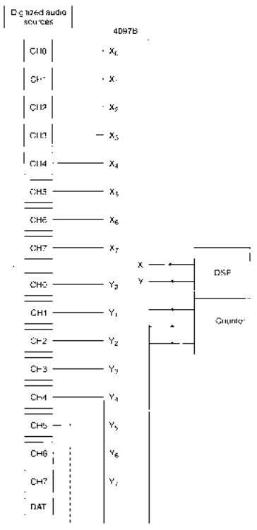
EXAMPLE 5.12 |
A CMOS 4097B dual 8-channel MUX/DMUX can be used simultaneously as a multi- |
|
plexer on one half of the device and as a demultiplexer on the other side. |
FIGURE 5.55 |
|
Example 5.12 |
|
4097B MUX/DMUX as a Time |
|
Division MUX/DMUX |
|

5.5 • Magnitude Comparators |
203 |
A circuit in a recording studio uses one side of a 4097B MUX/DMUX to multiplex 8 digital audio channels into a digital signal processor (DSP), using time division multiplexing. The other half of the 4097B takes the processed signals from a DSP output and distributes them to 8 channels on a digital audio tape (DAT) unit. Draw the circuit.
Solution Figure 5.55 shows a possible circuit. The counter can be part of the DSP. An audio source channel is selected by the counter inputs, data are sent to the DSP, where they are processed and sent to the same channel of the DAT. The counter advances by one, se-
lecting a new channel and repeating the process.
SomeanalogMUX/DMUXdevicesinhigh-speedCMOSinclude:74HC40518-channel MUX/DMUX, 74HC4052 dual 4-channel MUX/DMUX, and 74HC4053 triple 2-channel MUX/DMUX.
5.5 Magnitude Comparators
K E Y T E R M S
Magnitude comparator A circuit that compares two n-bit binary numbers, indi-
cates whether or not the numbers are equal, and, if not, which one is larger.
FIGURE 5.56
Exclusive NOR Gate
Table 5.11 |
XNOR |
Truth Table |
|
|
|
|
|
|
A |
B |
|
Y |
|
|
|
|
0 |
0 |
|
1 |
0 |
1 |
|
0 |
1 |
0 |
|
0 |
1 |
1 |
|
1 |
|
|
|
|
If we are interested in finding out whether or not two binary numbers are the same, we can use a magnitude comparator. The simplest comparison circuit is the Exclusive NOR gate, whose circuit symbol is shown in Figure 5.56 and whose truth table is given in Table 5.11.
The output of the XNOR gate is 1 if its inputs are the same (A B, symbolized AEQB) and 0 if they are different. For this reason, the XNOR gate is sometimes called a coincidence gate.
We can use several XNORs to compare each bit of two multi-bit binary numbers. Figure 5.57 shows a 2-bit comparator with one output that goes HIGH if all bits of A and B are identical.
FIGURE 5.57
2-bit Magnitude Comparator
If the most significant bit (MSB) of A equals the MSB of B, the output of the upper XNOR is HIGH. If the least significant bits (LSBs) are the same, the output of the lower XNOR is HIGH. If both these conditions are satisfied, then A B, which is indicated by a HIGH at the AND output. This general principle applies to any number of bits:
AEQB (An 1 |
Bn 1) (An 2 |
Bn 2) ... (A1 |
B1) (A0 B0) |
|
|
|
|
for two n-bit numbers, A and B.
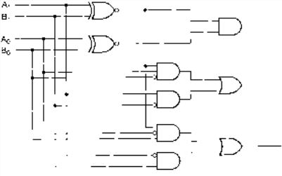
Some magnitude comparators also include an output that activates if A is greater than B (symbolized A B or AGTB) and another that is active when A is less than B (symbolized A B or ALTB). Figure 5.58 shows the comparator of Figure 5.57 expanded to include the “greater than” and “less than” functions.
Let us analyze the AGTB circuit. The AGTB function has two AND-shaped gates that compare A and B bit-by-bit to see which is larger.
204 C H A P T E R 5 • Combinational Logic Functions
FIGURE 5.58 |
|
2-bit Comparator With AEQB, |
|
AGTB, and ALTB Outputs |
AEQB |
AGTB
ALTB
1.The 2-input gate examines the MSBs of A and B. If A1 1 AND B1 0, then we know that A B. (This implies one of the following inequalities: 10 00; 10 01; 11 00; or 11 01.)
2.If A1 B1, then we don’t know whether or not A B until we compare the next most significant bits, A0 and B0. The 3-input gate makes this comparison. Since this gate is enabled by the XNOR, which compares the two MSBs, it is only active when A1 B1.
This yields the term (A B )A B in the Boolean expression for the AGTB function.
1 1 0 0
3.If A1 B1 AND A0 1 AND B0 0, then the 3-input gate has a HIGH output, telling us, via the OR gate, that A B. (The only possibilities are (01 00) and (11 10).)
Similar logic works in the ALTB circuit, except that inversion is on the A, rather than the B bits. Alternatively, we can simplify either the AGTB or the ALTB function by using a NOR function. For instance, if we have developed a circuit to indicate AEQB and ALTB, we can make the AGTB function from the other two, as follows:
AGTB AEQB ALTB
This Boolean expression implies that if A is not equal to or less than B, then it must be greater than B.
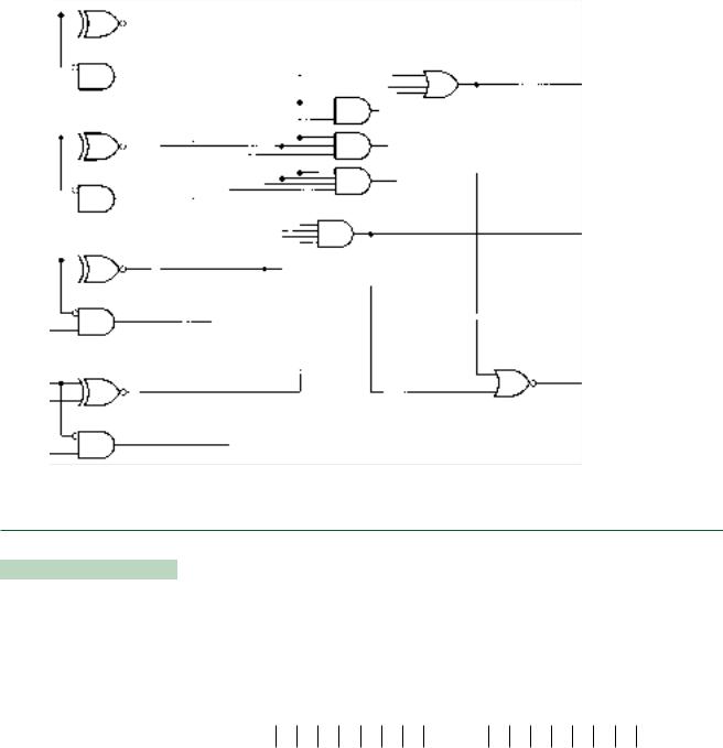
Figure 5.59 shows a 4-bit comparator with AEQB, ALTB, and AGTB outputs. The Boolean expressions for the outputs are:
AEQB (A3 B3)(A2 B2)(A1 B1)(A0 B0) |
|
|
|
|
|
(A3 B3) |
ALTB A3B3 (A3 B3)A2 |
B2 (A3 B3)(A2 B2)A1B1 |
|
|
|
|
|
(A2 B2)(A1 B1)A0B0 |
|
|
|
|
|
|
|
AGTB AEQB ALTB
This comparison technique can be expanded to as many bits as necessary. A 4-bit comparator requires four AND-shaped gates for its ALTB function. We can interpret the Boolean expression for this function as follows.
A B if:
1.The MSB of A is less than the MSB of B, OR
2.The MSBs are equal, but the second bit of A is less than the second bit of B, OR
3.The first two bits are equal, but the third bit of A is less than the third bit of B, OR
4.The first three bits are equal, but the LSB of A is less than the LSB of B
Expansion to more bits would use the same principle of comparing bits one at a time, beginning with the MSBs.
5.5 • Magnitude Comparators |
205 |
ALTB
AEQB
AGTB
FIGURE 5.59
4-bit Magnitude Comparator
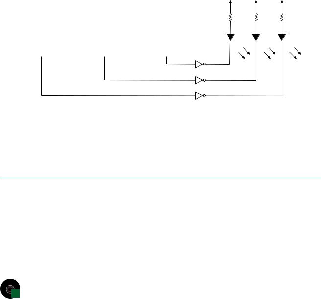
A digital thermometer has two input probes. A circuit in the thermometer converts the measured temperature at each probe to an 8-bit number, as shown by the block in Figure
|
|
|
|
A |
B |
|
|
Converter |
A7 A6 A5 A4 A3 A2 A1 A0 |
B7 B6 B5 B4 B3 B2 B1 B0 |
FIGURE 5.60
Example 5.13
Two-channel Digital Thermometer
5.60.
In addition to measuring the temperature at each input, the thermometer has a comparison function that indicates whether the temperature at one input is greater than, equal to, or less than the temperature at the other input.
Draw a logic diagram showing how a magnitude comparator could be connected to light a green LED for AGTB, an amber LED for AEQB, and a red LED for ALTB.
Solution Figure 5.61 shows the logic diagram of the magnitude comparator connected
206 |
|
C H A P T E R 5 • Combinational Logic Functions |
|
|
|
|
|
|
|
|
|
|
|
|
Probe |
|
|
|
|
Probe |
|
|
|
|
|
|
|
|
|
|
|
|
input |
|
|
|
|
input |
|
|
|
|
|
|
|
|
|
|
|
|
|
|
|
|
|
|
|
|
|
|
|
|
|
|
|
|
|
|
|
Vcc |
|
Vcc |
|
Vcc |
|
|
|
|
|
|
|
|
|
|
|
|
|
|
|
|
|
|
|
|
|
|
|
|
|
|
|
|
|
|
A |
|
|
|
|
|
B |
|
|
|
|
|
|
|
|
|
|
|
Converter |
|
|
|
|
|
|
|
|
|
A7 A6 A5 A4 A3 A2 A1 A0 |
|
B7 B6 B5 B4 B3 B2 B1 B0 |
|
|
|
|
|
|
|
|
|
|
|
|
|
|
|
|
|
|
|
|
|
|
|
|
|
|
|
|
|
|
|
|
|
|
|
|
|
|
|
A7 A6 A5 A4 A3 A2 A1 A0 |
|
B7 B6 B5 B4 B3 B2 B1 B0 |
G |
A |
R |
|
|
|
|
|
|
|
|
|
|
Comparator |
|
|
|
|
|
|
|
|
|
|
|
ALTB |
AEQB |
|
|
|
|
|
|
AGTB |
|
|
|
|
|
|
|
|
|
|
|
|
|
|
|
|
|
|
|
|
|
|
|
|
|
|
|
|
|
|
|
|
|
|
|
|
|
|
FIGURE 5.61
Example 5.13
Temperature Comparator Block Diagram
to the thermometer’s digital output.
When one of the comparator outputs goes HIGH, it sets the output of the corresponding inverter LOW. This provides a current path to ground for the indicator LED for that
output, causing it to illuminate. |
|
|
compare2.vhd
compare2.scf
VHDL Magnitude Comparators
The most obvious way to create a VHDL representation of a magnitude comparator is to use a concurrent signal assignment statement for each comparing function. For example, the following VHDL code can represent the 2-bit magnitude comparator of Figure 5.57:
—— compare2.vhd
ENTITY compare2 IS
PORT(
a, b : IN BIT_VECTOR (1 downto 0); agtb, aeqb, altb : OUT BIT);
END compare2;
ARCHITECTURE a OF compare2 IS
BEGIN
altb |
<= |
(not (a(1)) |
and b(1)) |
|
|
or |
((not (a(1) |
xor b(1))) and (not (a(0)) and b(0))); |
aeqb |
<= |
(not (a(1) xor b(1))) and (not (a(0) |
xor b(0))); |
agtb |
<= |
(a(1) |
and not (b(1))) |
|
|
or |
((not |
(a(1) |
xor b(1))) and (a(0) and |
not (b(0)))); |
END a;
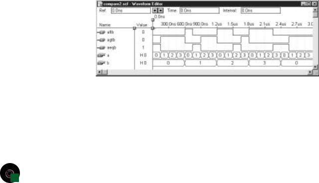
A simulation for this file is shown in Figure 5.62. The comparison outputs go HIGH to indicate A B, A B, or A B.
Although this approach works, it is not a very good one. Due to the complexity of the Boolean equations for ALTB and AGTB, it is difficult to type them without making errors. (Try it!) The difficulty increases greatly with the number of required inputs.
5.5 • Magnitude Comparators |
207 |
FIGURE 5.62
Simulation for a 2-bit Magnitude Comparator
The following code for a 4-bit comparator illustrates a much more efficient method. Since VHDL allows inputs to be represented as integers, we can define the required size of inputs A and B and compare them using IF statements. For every comparison, we assign an output vector consisting of bits for ALTB, AEQB, and AGTB one of the values 110, 101, or 011, for active-LOW outputs. For example, if A 12 and B 9, then the output vector would be 011 (i.e., A B). An active-LOW output will illuminate a LOW-sense LED,
compare4.vhd
compare4.scf
LIBRARY ieee; |
|
|
USE ieee.std_logic_1164.ALL; |
|
ENTITY compare4 IS |
|
|
PORT( |
|
|
a, b |
: IN |
INTEGER RANGE 0 TO 15; |
agtb, aeqb, altb : OUT |
STD_LOGIC); |
END compare4; |
|
|
ARCHITECTURE a OF compare4 IS
SIGNAL compare : STD_LOGIC_VECTOR (2 downto 0);
BEGIN |
|
|
|
PROCESS (a,b) |
|
|
BEGIN |
|
|
|
IF a<b THEN |
|
compare |
<= |
“110”; |
ELSIF a=b THEN |
|
compare |
<= |
“101”; |
ELSIF a>b THEN |
|
compare |
<= |
“011”; |
ELSE |
|
|
|
compare |
<= |
“111”; |
END IF; |
|
|
|
agtb |
<= |
compare(2); |
aeqb |
<= |
compare(1); |
altb |
<= |
compare(0); |
END PROCESS;
END a;
The beauty of this method is that the number of input bits can be changed by modifying one number: the range of the INTEGER-type input. For example, a 12-bit comparator is identical to the 4-bit comparator in the previous VHDL code, except that the inputs have a range of 0 to 4095 ( 212 1). Using this method, we can program an EPM7128S CPLD
C H A P T E R 5 • Combinational Logic Functions
with a comparator up to 28 bits wide (range of 0 to 268,435,455). If we do, however, there is no room for anything else.
5.14Write a VHDL file that uses IF statements to compare two 8-bit numbers A and B. The design should have outputs for AEQB, ALTB, and AGTB.
Solution
—— compare8.vhd |
|
|
LIBRARY ieee; |
|
|
USE ieee.std_logic_1164.ALL; |
|
ENTITY compare8 IS |
|
|
PORT( |
|
|
a, b |
: IN |
INTEGER RANGE 0 TO 255; |
compare8.vhd
ARCHITECTURE a OF compare8 IS
SIGNAL compare : STD_LOGIC_VECTOR (2 downto 0);
BEGIN |
|
|
|
PROCESS (a,b) |
|
|
BEGIN |
|
|
|
IF a<b THEN |
|
|
|
compare |
<= |
“110”; |
ELSIF a=b THEN |
|
|
|
compare |
<= |
“101”; |
ELSIF a>b THEN |
|
|
|
compare |
<= |
“011”; |
ELSE |
|
|
|
|
compare |
<= |
“111”; |
END IF; |
|
|
agtb |
<= compare(2); |
aeqb |
<= compare(1); |
altb |
<= compare(0); |
END PROCESS;
END a;
5.6 Parity Generators and Checkers
K E Y T E R M S
Parity A system that checks for errors in a multi-bit binary number by counting the number of 1s.
Even parity An error-checking system that requires a binary number to have an even number of 1s.
Odd parity An error-checking system that requires a binary number to have an odd number of 1s.
Parity bit A bit appended to a binary number to make the number of 1s even or odd, depending on the type of parity.
When data are transmitted from one device to another, it is necessary to have a system of checking for errors in transmission. These errors, which appear as incorrect bits, occur as a result of electrical limitations such as line capacitance or induced noise.
5.6 • Parity Generators and Checkers |
209 |
FIGURE 5.63
Parity Error Checking
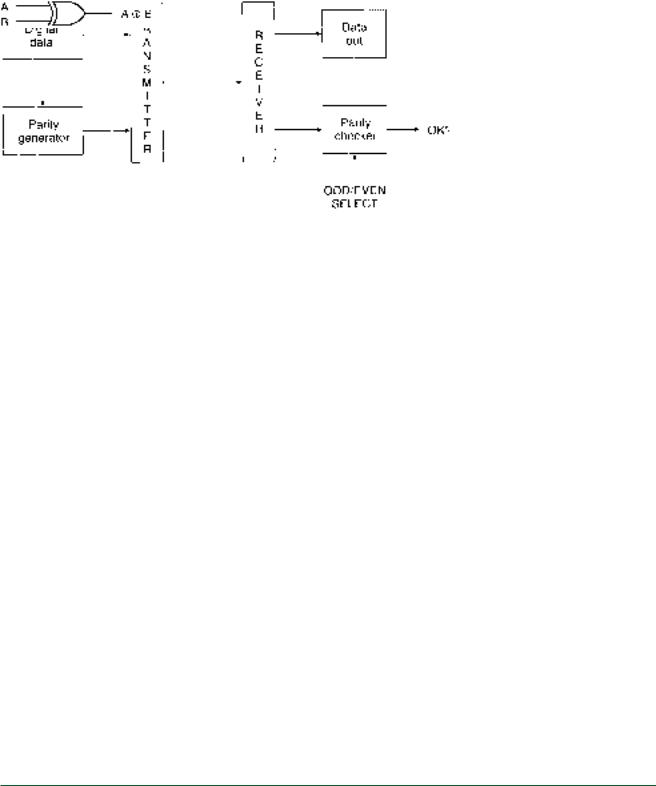
Parity error checking is a way of encoding information about the correctness of data before they are transmitted. The data can then be verified at the system’s receiving end. Figure 5.63 shows a block diagram of a parity error-checking system.
|
|
The parity generator in Figure 5.63 examines the outgoing data and adds a bit called |
|
the parity bit that makes the number of 1s in the transmitted data odd or even, depending |
|
on the type of parity. Data with EVEN parity have an even number of 1s, including the |
|
parity bit, and data with ODD parity have an odd number of 1s. |
|
|
The data receiver “knows” whether to expect EVEN or ODD parity. If the incoming |
|
number of 1s matches the expected parity, the parity checker responds by indicating that |
|
correct data have been received. Otherwise, the parity checker indicates an error. |
|
|
EXAMPLE 5.16 |
Data are transmitted from a PC serial port to a modem in groups of 7 data bits plus a parity |
|
bit. What should the parity bit, P, be for each of the following data if the parity is EVEN? |
|
If the parity is ODD? |
|
a. |
0110110 |
|
b. |
1000000 |
|
c. |
0010101 |
Solution
a. 0110110 Four 1s in data. (4 is an even number.) EVEN parity: P 0
ODD parity: P 1
b. 1000000 One 1 in data. (1 is an odd number.) EVEN parity: P 1
ODD parity: P 0
c. 0010101 Three 1s in data. (3 is an odd number.) EVEN parity: P 1
ODD parity: P 0
FIGURE 5.64
Exclusive OR Gate
An Exclusive OR gate can be used as a parity generator or a parity checker. Figure 5.64 shows the gate, and Table 5.12 is the XOR truth table. Notice that each line of the XOR truth table has an even number of 1s if we include the output column.
Figure 5.65 shows the block diagram of a circuit that will generate an EVEN parity bit from 2 data bits, A and B, and transmit the three bits one after the other, that is, serially, to a data receiver.