

Digital design with CPLD applications and VHDL (R. Dueck, 2000)
.pdf100 C H A P T E R 3 • Boolean Algebra and Combinational Logic
This expands to the following expression:
Y A B C (D D) A (B B) C D (A A) B C D A B C D
A B C D A B C D A B C D A B C D A B C D
A B C D A B C D
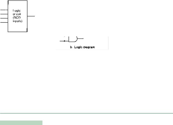
This expression can be loaded directly into the K-map and simplified, as shown in Figure 3.54b. The logic diagram for the simplified expression is shown in Figure 3.55.
FIGURE 3.55
Example 3.20
Simplified Circuit
Don’t Care States
K E Y T E R M S
Don’t care state An output state that can be regarded as either HIGH or LOW, as is most convenient. A don’t care state is the output state of a circuit for a combination of inputs that will never occur.
Sometimes a digital circuit will be intended to work only for certain combinations of inputs; any other input values will never be applied to the circuit.
In such a case, it may be to our advantage to use so-called don’t care states to simplify the circuit. A don’t care state is shown in a K-map cell as an “X” and can be either a 0 or a 1, depending on which case will yield the maximum simplification.
A common application of the don’t care state is a digital circuit designed for binarycoded decimal (BCD) inputs. In BCD, a decimal digit (0–9) is encoded as a 4-bit binary number (0000–1001). This leaves six binary states that are never used (1010, 1011, 1100, 1101, 1110, 1111). In any circuit designed for BCD inputs, these states are don’t care
|
states. |
|
All cells containing 1s must be grouped if we are looking for a maximum SOP simpli- |
|
fication. (If necessary, a group can contain one cell.) The don’t care states can be used to |
|
maximize the size of these groups. We need not group all don’t care states, only those that |
|
actually contribute to a maximum simplification. |
|
|
EXAMPLE 3.21 |
The circuit in Figure 3.56 is designed to accept binary-coded decimal inputs. The output is |
|
HIGH when the input is the BCD equivalent of 5, 7, or 9. If the BCD equivalent of the in- |
|
put is not 5, 7 or 9, the output is LOW. The output is not defined for input values greater |
|
than 9. |
|
Find the maximum SOP simplification of the circuit. |
D1
D2
D3
D4
FIGURE 3.56
Example 3.21
Circuit to be Simplified
3.5 • Simplification by the Karnaugh Map Method |
101 |
Solution The Karnaugh map for the circuit is shown in Figure 3.57a.
We can designate three of the don’t care cells as 1s—those corresponding to input states 1011, 1101, and 1111. This allows us to group the 1s into two overlapping quads, which yield the following simplification.
Y D4 D1 D3 D1
The ungrouped don’t care states are treated as 0s. The corresponding circuit is shown in Figure 3.57b.
FIGURE 3.57
Example 3.21
Karnaugh Map and Logic
Diagram
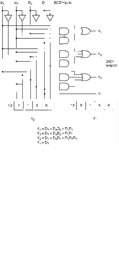
EXAMPLE 3.22
Applications
One type of decimal code is called 2421 code, so called because of the positional weights of its bits. (For example, 1011 in 2421 code is equivalent to 2 2 1 5 in decimal. 1100 is equivalent to decimal 2 4 6.) Table 3.16 shows how this code compares to its equivalent decimal digits and to the BCD code used in Example 3.21.
2421 code is sometimes used because it is “self-complementing,” a property that BCD code does not have, but that is useful in digital decimal arithmetic circuits.
The bits of the BCD code are designated D4 D3 D2 D1. The bits of the 2421 code are
designated Y4 Y3 Y2 Y1.
Use the Karnaugh map method to design a logic circuit that accepts any BCD input and generates an output in 2421 code, as specified by Table 3.16.
Solution The required circuit is called a code converter. Each 4-bit BCD input corresponds to a 4-bit 2421 output. Thus, we must find four Boolean expressions, one for each
Table 3.16 BCD and 2421 Code
Decimal |
|
BCD Code |
|
|
2421 Code |
|
||
Equivalent |
D4 |
D3 |
D2 |
D1 |
Y4 |
Y3 |
Y2 |
Y1 |
|
|
|
|
|
|
|
|
|
0 |
0 |
0 |
0 |
0 |
0 |
0 |
0 |
0 |
1 |
0 |
0 |
0 |
1 |
0 |
0 |
0 |
1 |
2 |
0 |
0 |
1 |
0 |
0 |
0 |
1 |
0 |
3 |
0 |
0 |
1 |
1 |
0 |
0 |
1 |
1 |
4 |
0 |
1 |
0 |
0 |
0 |
1 |
0 |
0 |
5 |
0 |
1 |
0 |
1 |
1 |
0 |
1 |
1 |
6 |
0 |
1 |
1 |
0 |
1 |
1 |
0 |
0 |
7 |
0 |
1 |
1 |
1 |
1 |
1 |
0 |
1 |
8 |
1 |
0 |
0 |
0 |
1 |
1 |
1 |
0 |
9 |
1 |
0 |
0 |
1 |
1 |
1 |
1 |
1 |
|
|
|
|
|
|
|
|
|
102 C H A P T E R 3 • Boolean Algebra and Combinational Logic
FIGURE 3.58
Example 3.22
K-Maps: BCD to 2421
FIGURE 3.59
Example 3.22
BCD-to-2421 Code Converter
3.5 • Simplification by the Karnaugh Map Method |
103 |
bit of the 2421 code. We can derive each Boolean expression from a truth table represented by the corresponding output column in Table 3.16.
We can load the 2421 values into four different Karnaugh maps, as shown in Figure 3.58. The cells corresponding to the unused input BCD codes 1010, 1011, 1100, 1101, 1110, and 1111 are don’t care states in each map.
The K-maps yield the following simplifications:
Y4 D4 D3 D2 D3 D1
Y3 D4 D3 D2 D3 D1 Y2 D4 D3 D2 D3 D2 D1 Y1 D1
Figure 3.59 shows the logic diagram for these equations.
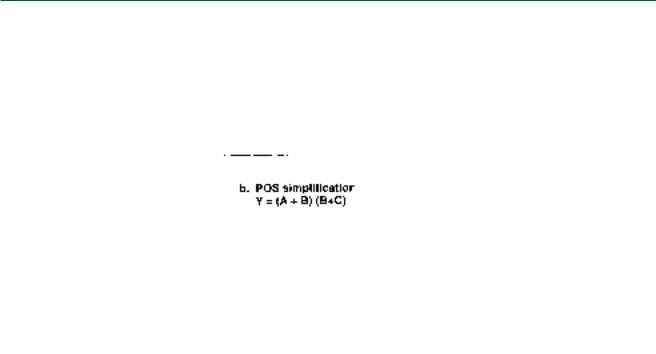
POS Simplification
Until now, we have looked only at obtaining the maximum SOP simplification from a Karnaugh map. It is also possible to find the maximum POS simplification from the same map.
Figure 3.60 shows a Karnaugh map with the cells grouped for an SOP simplification and a POS simplification. The SOP simplification is shown in Figure 3.60a and the POS simplification in Figure 3.60b.
FIGURE 3.60
SOP and POS Forms on a
K-Map
When we derive the POS form of an expression from a truth table, we use the lines where the output is 0 and we use the complements of the input variables on these lines as the elements of the selected maxterms. The same principle applies here.
The maxterms are:
(A B C) |
Top left cell |
(A B C) |
Bottom left cell |
(A B C) |
Bottom right cell |
The variables are canceled in much the same way as in the SOP form. Remember, however, that the POS variables are the complements of the variables written beside the Karnaugh map.
If there is more than one simplified term, the terms are ANDed together, as in a full POS form.
Cancellations:
Outside pair: |
A is present in both true and complement form in the pair. (Dis- |
|
card A.) |
|
B and C are present in both cells of the pair. (Keep B and C.) |
|
Term: B C |

104 C H A P T E R 3 • Boolean Algebra and Combinational Logic
Bottom pair: A and B are present in both cells of the pair. (Keep A and B.)
C is present in both true and complement form in the pair. (Discard C.)
Term: A B
Maximum POS simplification:
Y (A B)(B C)
Compare this with the maximum SOP simplification:
Y A C B
By the Boolean theorem (x y)(x z) x yz, we see that the SOP and POS forms are equivalent.
EXAMPLE 3.23
Table 3.17 Truth Table for Example 3.23
Find the maximum POS simplification of the logic function represented by Table 3.17.
Solution Figure 3.61 shows the Karnaugh map from the truth table in Table 3.17. The cells containing 0s are grouped in two quads and there is a single 0 cell left over.
Simplification:
|
|
|
|
|
Corner quad: |
(B D) |
|
|
A |
B |
C |
D |
Y |
|
|||
Horizontal quad: |
(A B) |
|
||||||
|
|
|
|
|
|
|||
0 |
0 |
0 |
0 |
0 |
Single cell: |
(A B C D) |
|
|
0 |
0 |
0 |
1 |
0 |
Y (A B)(B D)(A B C D) |
|
||
0 |
0 |
1 |
0 |
0 |
|
|||
|
|
|||||||
0 |
0 |
1 |
1 |
0 |
|
|
|
|
0 |
1 |
0 |
0 |
1 |
FIGURE 3.61 |
|
|
|
0 |
1 |
0 |
1 |
1 |
Example 3.23 |
|
|
|
0 |
1 |
1 |
0 |
1 |
POS Simplification of Table 3.17 |
|
||
0 |
1 |
1 |
1 |
1 |
|
|
|
|
1 |
0 |
0 |
0 |
0 |
|
|
|
|
1 |
0 |
0 |
1 |
1 |
|
|
|
|
1 |
0 |
1 |
0 |
0 |
|
|
|
|
1 |
0 |
1 |
1 |
1 |
|
|
|
|
1 |
1 |
0 |
0 |
1 |
|
|
|
|
1 |
1 |
0 |
1 |
0 |
|
|
|
|
1 |
1 |
1 |
0 |
1 |
|
|
|
|
1 |
1 |
1 |
1 |
1 |
|
|
|
|
|
|
|
|
|
|
|
|
|
S U M M A R Y
1. Two or more gates connected together form a logic gate network or combinational logic circuit, which can be described by a truth
table, a logic diagram, or a Boolean expression.
2.The output of a combinational logic circuit is always the same with the same combination of inputs, regardless of the order in which they are applied.
3.The order of precedence in a logic gate network is AND, then OR, unless otherwise indicated by parentheses.
4.DeMorgan’s theorems: x y x y
x y x y
5. Inequalities: x y x y
x y x y
6.A logic gate network can be drawn to simplify its Boolean expression by ensuring that bubbled (active-LOW) outputs drive bubbled inputs and outputs with no bubble (activeHIGH) drive inputs with no bubble. Some gates might need to be drawn in their DeMorgan equivalent form to achieve this.
7.In Boolean expressions, logic inversion bars of equal lengths

cancel; bars of unequal lengths do not. Bars of equal length represent bubble-to-bubble connections.
8.A logic diagram can be derived from a Boolean expression by order of precedence rules: synthesize ANDs before ORs, unless parentheses indicate otherwise. Inversion bars act as parentheses for a group of variables.
9.A truth table can be derived from a logic gate network either by finding truth tables for intermediate points in the network and combining them by the laws of Boolean algebra, or by simplifying the Boolean expression into a form that can be directly written into a truth table.
10.A sum-of-products (SOP) network combines inputs in AND gates to yield a group of product terms that are combined in an OR gate (logical sum) output.
11.A product-of-sums (POS) network combines inputs in OR gates to yield a group of sum terms that are combined in an AND gate (logical product) output.
12.An SOP Boolean expression can be derived from the lines in a truth table where the output is at logic 1. Each product term contains all inputs in true or complement form, where inputs at logic 0 have a bar and inputs at logic 1 do not.
13.A POS expression is derived from the lines where the output is at logic 0. Each sum term contains all inputs in true or complement form, where inputs at logic 1 have a bar and inputs at logic 0 do not.
14.Theorems of Boolean algebra, summarized in Table 3.8, allow us to simplify logic gate networks.
15.SOP networks can be simplified by grouping pairs of product terms and applying the Boolean identity xyz xyz xy.
16.POS networks can be simplified by grouping pairs of sum terms and applying the Boolean identity (x y z) (x y z) (x y).
Glossary 105
17.To achieve maximum simplification of an SOP or POS network, each product or sum term should be grouped with another if possible. A product or sum term can be grouped more than once, as long as each group has a term that is only in that group.
18.A Karnaugh map can be used to graphically reduce a Boolean expression to its simplest form by grouping adjacent cells containing 1s. One cell is equivalent to one line of a truth table. A group of adjacent cells that contain 1s represents a simplified product term.
19.Adjacent cells in a K-map differ by only one variable. Cells around the outside of the map are considered adjacent.
20.A group in a K-map must be a power of two in size: 1, 2, 4, 8, or 16. A group of two is called a pair, a group of four is a quad, and a group of eight is an octet.
21.A pair cancels one variable. A quad cancels two variables. An octet cancels three variables.
22.A K-map can have multiple groups. Each group represents one simplified product term in a sum-of-products expression.
23.Groups in K-maps can overlap as long as each group has one or more cells that appear only in that group.
24.Groups in a K-map should be as large as possible for maximum SOP simplification.
25.Don’t care states represent output states of input combinations that will never occur in a circuit. They are represented by Xs in a truth table or K-map and can be used as 0s or 1s, whichever is most advantageous for the simplification of the circuit.
G L O S S A R Y
Adjacent cell Two cells are adjacent if there is only one variable that is different between the coordinates of the two cells.
Associative property A mathematical function is associative if its operands can be grouped in any order without affecting the result.
For example, addition is associative ((a b) c a (b c)), but subtraction is not ((a b) c a (b c)).
Bubble-to-bubble convention The practice of drawing gates in a logic diagram so that inverting outputs connect to inverting inputs and noninverting outputs connect to noninverting inputs.
Bus form A way of drawing a logic diagram so that each true and complement input variable is available along a conductor called a bus.
Cell The smallest unit of a Karnaugh map, corresponding to one line of a truth table. The input variables are the cell’s coordinates and the output variable is the cell’s contents.
Combinational logic Digital circuitry in which an output is derived from the combination of inputs, independent of the order in which they are applied.
Combinatorial logic Another name for combinational logic.
Commutative property A mathematical operation is commutative if it can be applied to its operands in any order without affecting the result. For example, addition is commutative (a b b a), but subtraction is not (a b b a).
Distributive property Full name: distributive property of multiplication over addition. The property that allows us to distrib-
ute (“multiply through”) an AND across several OR functions. For example, a(b c) ac bc.
Don’t care state An output state that can be regarded either as HIGH or LOW, as is most convenient. A don’t care state is the output state of a circuit for a combination of inputs that will never occur.
Karnaugh map A graphical tool for finding the maximum SOP or POS simplification of a Boolean expression. A Karnaugh map works by arranging the terms of an expression in such a way that variables can be cancelled by grouping minterms or maxterms.
Levels of gating The number of gates through which a signal must pass from input to output of a logic gate network.
Logic diagram A diagram, similar to a schematic, showing the connection of logic gates.
Logic gate network Two or more logic gates connected together.
Maximum POS simplification The form of a POS Boolean expression which cannot be further simplified by cancelling variables in the sum terms. It may be possible to get an SOP form with fewer terms or variables.
106 C H A P T E R 3 • Boolean Algebra and Combinational Logic
Maximum SOP simplification The form of an SOP Boolean expression which cannot be further simplified by cancelling variables in the product terms. It may be possible to get a POS form with fewer terms or variables.
Maxterm A sum term in a Boolean expression where all possible variables appear once in true or complement form.
Minterm A product term in a Boolean expression where all possible variables appear once in true or complement form.
Octet A group of eight cells in a Karnaugh map. An octet cancels three variables in a K-map simplification.
Order of precedence The sequence in which Boolean functions are performed, unless otherwise specified by parentheses.
Pair A group of two cells in a Karnaugh map. A pair cancels one variable in a K-map simplification.
Product term A term in a Boolean expression where one or more true or complement variables are ANDed.
Truth Tables
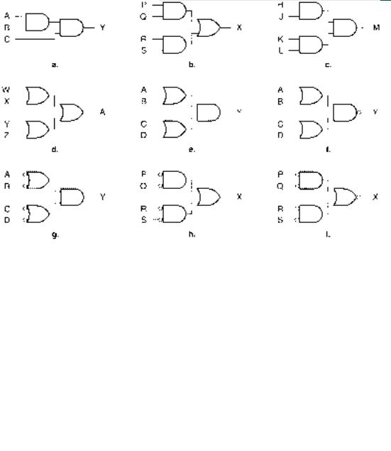
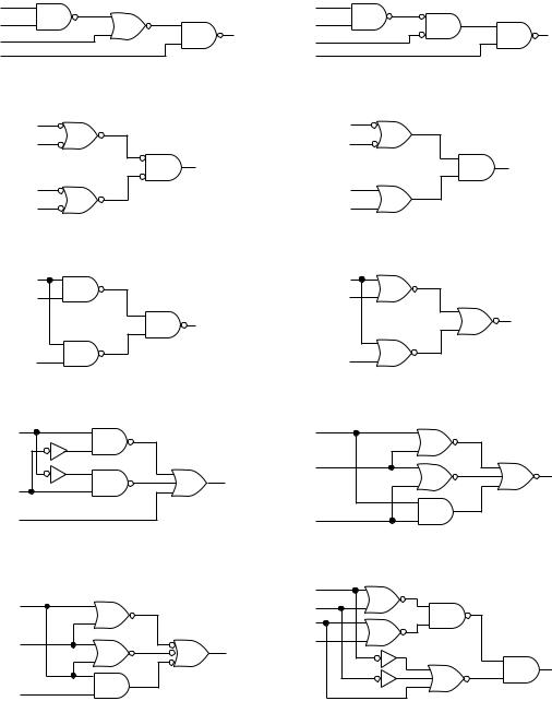
3.1Write the unsimplified Boolean expression for each of the logic gate networks shown in Figure 3.62.
3.2Write the unsimplified Boolean expression for each of the logic gate networks shown in Figure 3.63.
3.3Redraw the logic diagrams of the gate networks shown in Figure 3.63 a, e, f, h, i, and j so that they conform to the
FIGURE 3.62
Problem 3.1
Logic Circuits
Product-of-sums (POS) A type of Boolean expression where several sum terms are multiplied (ANDed) together.
Quad A group of four cells in a Karnaugh map. A quad cancels two variables in a K-map simplification.
Sum term A term in a Boolean expression where one or more true or complement variables are ORed.
Sum-of-products (SOP) A type of Boolean expression where several product terms are summed (ORed) together.
Synthesis The process of creating a logic circuit from a description such as a Boolean equation or truth table.
P R O B L E M S
Problem numbers set in color indicate more difficult problems: those with underlines indicate most difficult problems.
Section 3.1 Boolean Expressions, Logic Diagrams, and
|
|
Problems |
107 |
bubble-to-bubble convention. Rewrite the Boolean ex- |
3.4 |
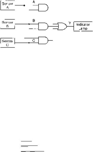
The circuit in Figure 3.64 is called a majority vote circuit. |
|
pression of each of the redrawn circuits. |
|
It will turn on an active-HIGH indicator lamp only if a |
|
|
|
majority of inputs (two out of three) are HIGH. Write the |
|
|
|
Boolean expression for the circuit. |
|
T |
|
H |
U |
X |
J |
V |
M |
|
|
K |
|
W |
|
L |
a. |
|
b. |
Q |
|
Q |
R |
|
R |
X |
|
X |
S |
|
S |
T |
|
T |
|
|
|
c. |
|
d. |
A |
|
A |
B |
|
B |
Y |
|
Y |
|
|
|
C |
|
C |
e. |
|
f. |
J |
|
A |
|
|
B |
|
M |
Y |
K |
|
|
|
|
|
L |
|
C |
g. |
|
h. |
|
|
A |
A |
|
B |
|
|
C |
B |
Y |
D |
|
|
|
|
|
Y |
C |
|
|
i. |
|
j. |
FIGURE 3.63
Problem 3.2
Logic Circuits
108 C H A P T E R 3 • Boolean Algebra and Combinational Logic
3.5Suppose you wish to design a circuit that indicates when three out of four inputs are HIGH. The circuit has four in-
puts, D3, D2, D1, and D0 and an active-HIGH output, Y. Write the Boolean expression for the circuit and draw the
function represented by the following truth table. Draw the logic diagram for each form.
3.12Find the Boolean expression, in both sum-of-products (SOP) and product-of-sums (POS) forms, for the logic function represented by the following truth table. Draw the logic diagram for the SOP form only.
FIGURE 3.64
Problem 3.4
Majority Vote Circuit
logic circuit.
3.6Draw the logic circuit for each of the following Boolean expressions:
a.Y AB BC
b.Y ACD BCD
c.Y (A B)(C D)
d.Y A BC D
e.Y AC B C
f.Y AC B C
g.Y ABD BC A C
h.Y AB AC BC
i.Y AB AC BC
3.7Use DeMorgan’s theorems to modify the Boolean equations in Problem 3.6, parts e, f, g, h, and i so that there is no bar over any group of variables. Redraw the logic diagrams of the circuits to reflect the changes. (The final circuit versions should conform to the bubble-to-bubble convention.)
3.8Write the truth tables for the logic diagrams in Figure 3.62, parts b, e, f, and g.
3.9Write the truth tables for the logic diagrams in Figure 3.63, parts a, h, i, and j.
3.10Write the truth tables for the Boolean expression in Problem 3.6, parts c, d, e, f, h, and i.
Section 3.2 Sum-of-Products (SOP) and Product-of-
Sums (POS) Forms
3.11Find the Boolean expression, in both sum-of-products (SOP) and product-of-sums (POS) forms, for the logic
A |
B |
C |
|
Y |
|
|
|
|
|
0 |
0 |
0 |
|
1 |
0 |
0 |
1 |
|
1 |
0 |
1 |
0 |
|
1 |
0 |
1 |
1 |
|
1 |
1 |
0 |
0 |
|
0 |
1 |
0 |
1 |
|
0 |
1 |
1 |
0 |
|
0 |
1 |
1 |
1 |
|
0 |
|
3.13Find the Boolean expression, in both sum-of-products (SOP) and product-of-sums (POS) forms, for the logic function represented by the following truth table. Draw the logic diagram for the POS form only.
A |
B |
C |
|
Y |
|
|
|
|
|
0 |
0 |
0 |
|
0 |
0 |
0 |
1 |
|
1 |
0 |
1 |
0 |
|
0 |
0 |
1 |
1 |
|
0 |
1 |
0 |
0 |
|
1 |
1 |
0 |
1 |
|
0 |
1 |
1 |
0 |
|
1 |
1 |
1 |
1 |
|
0 |
|
3.14Find the Boolean expression, in both sum-of-products (SOP) and product-of-sums (POS) forms, for the logic function represented by the following truth table. Draw the logic diagram for the SOP form only.
A |
B |
C |
|
Y |
|
|
|
|
|
0 |
0 |
0 |
|
0 |
0 |
0 |
1 |
|
1 |
0 |
1 |
0 |
|
1 |
0 |
1 |
1 |
|
0 |
1 |
0 |
0 |
|
0 |
1 |
0 |
1 |
|
1 |
1 |
1 |
0 |
|
1 |
1 |
1 |
1 |
|
1 |
|
3.15Write the POS form of the 2-input XOR function. Draw the logic diagram of the POS form of the XOR function.
3.16Write the POS form of the 2-input XNOR function. Draw the logic diagram of the POS form of the XNOR func-
A |
B |
C |
D |
|
Y |
|
|
|
|
|
|
0 |
0 |
0 |
0 |
|
0 |
0 |
0 |
0 |
1 |
|
0 |
0 |
0 |
1 |
0 |
|
0 |
0 |
0 |
1 |
1 |
|
0 |
0 |
1 |
0 |
0 |
|
1 |
0 |
1 |
0 |
1 |
|
0 |
0 |
1 |
1 |
0 |
|
1 |
0 |
1 |
1 |
1 |
|
0 |
1 |
0 |
0 |
0 |
|
1 |
1 |
0 |
0 |
1 |
|
0 |
1 |
0 |
1 |
0 |
|
0 |
1 |
0 |
1 |
1 |
|
0 |
1 |
1 |
0 |
0 |
|
0 |
1 |
1 |
0 |
1 |
|
1 |
1 |
1 |
1 |
0 |
|
0 |
1 |
1 |
1 |
1 |
|
0 |
|
tion.
Section 3.3 Theorems of Boolean Algebra
3.17Write the Boolean expression for the circuit shown in Figure 3.65 Use the distributive property to transform the circuit into a sum-of-products (SOP) circuit.
3.18Write the Boolean expression for the circuit shown in Figure 3.66 Use the distributive property to transform the circuit into a sum-of-products (SOP) circuit.
3.19Use the rules of Boolean algebra to simplify the follow-
A
B |
Y |
C |
D
FIGURE 3.65
Problem 3.17
Logic Circuit
ing expressions as much as possible.
a. Y A A B C
A
B
C
D
E
F
FIGURE 3.66
Problem 3.18
Logic Circuit
Problems 109
b.Y A A B C
c.J K L L
d.S (T U) V V
e.S T V V
f.Y (A B C)(B D F)
3.20Use the rules of Boolean algebra to simplify the following expressions as much as possible.
a.M P Q P Q R
b.M P Q P Q R
c.S (T U ) V (T U)
d.Y (A B D) A C A B D
e.Y (A B D) A C A B D
f.P (Q R S T )(Q R Q)
g.U (X Y W Z)(W Y Y W Z)
3.21Use the rules of Boolean algebra to simplify the following expressions as much as possible.
a.Y A B C D (A B) C D A B
b.Y A B C D (A B) C D A B
c.K (L M L M )(M N L M N) M(N L)
Section 3.4 Simplifying SOP and POS Expressions
3.22Use the rules of Boolean algebra to find the maximum SOP and POS simplifications of the function represented by the following truth table.
3.23Use the rules of Boolean algebra to find the maximum SOP and POS simplifications of the function represented by the following truth table.
A |
B |
C |
|
Y |
|
|
|
|
|
0 |
0 |
0 |
|
0 |
0 |
0 |
1 |
|
1 |
0 |
1 |
0 |
|
0 |
0 |
1 |
1 |
|
1 |
1 |
0 |
0 |
|
0 |
1 |
0 |
1 |
|
1 |
1 |
1 |
0 |
|
0 |
1 |
1 |
1 |
|
1 |
|
3.24Use the rules of Boolean algebra to find the maximum SOP and POS simplifications of the function represented by the following truth table.
A |
B |
C |
|
Y |
|
|
|
|
|
0 |
0 |
0 |
|
1 |
0 |
0 |
1 |
|
0 |
0 |
1 |
0 |
|
1 |
0 |
1 |
1 |
|
0 |
1 |
0 |
0 |
|
0 |
1 |
0 |
1 |
|
0 |
1 |
1 |
0 |
|
1 |
1 |
1 |
1 |
|
0 |
|