

Digital design with CPLD applications and VHDL (R. Dueck, 2000)
.pdf40 |
C H A P T E R |
2 • Logic Functions and Gates |
|
|
|
|
|
|
|
As previously stated, any ANDor OR-shaped gate can be represented in its DeMor- |
|||||
|
|
gan equivalent form. All we need to do is analyze a gate for its shape, input, and output, |
|||||
|
|
then change everything. |
|
|
|
|
|
|
|
|
|
|
|
||
|
EXAMPLE 2.3 |
Analyze the gate in Figure 2.25 and write a Boolean expression, descriptive sentence, and |
|||||
|
|
truth table for the gate. Mark active output levels on the truth table with asterisks. Find the |
|||||
|
|
DeMorgan equivalent form of the gate and write its Boolean expression and description. |
|||||
|
|
FIGURE 2.25 |
A |
|
|
|
|
|
|
|
|
|
|
||
|
|
Example 2.3: Logic Gates |
B |
|
|
|
Y |
|
|
|
|
|
|||
|
|
|
C |
|
|
|
|
SOLUTION
Boolean expression: Y A B C
Shape: OR (at least one)
Input: LOW
Output: LOW
Descriptive sentence: Output Y is LOW if A OR B OR C is LOW.
Truth table: |
Table 2.14 |
Truth Table |
|||
|
of Gate in Figure 2.25 |
|
|||
|
|
|
|
|
|
|
A |
B |
C |
|
Y |
|
|
|
|
|
|
|
0 |
0 |
0 |
|
0* |
|
0 |
0 |
1 |
|
0* |
|
0 |
1 |
0 |
|
0* |
|
0 |
1 |
1 |
|
0* |
|
1 |
0 |
0 |
|
0* |
|
1 |
0 |
1 |
|
0* |
|
1 |
1 |
0 |
|
0* |
|
1 |
1 |
1 |
|
1 |
|
|
|
|
|
|
Figure 2.26 shows the DeMorgan equivalent form of the gate in Figure 2.25. To create this symbol, we change the shape from OR to AND and invert the logic levels at both input and output.
FIGURE 2.26 |
A |
|
|
|
|
|
|
|
|
||
Example 2.3: DeMorgan |
B |
|
|
|
Y |
|
|
|
|||
Equivalent of Gate in |
C |
|
|
|
|
|
|
|
|
||
|
|
|
|
|
|
Figure 2.25 |
|
|
|
|
|
Boolean expression: Y ABC
Descriptive sentence: Output Y is HIGH if A AND B AND C are HIGH.
SECTION 2.4 REVIEW PROBLEM
2.8 The output of a gate is described by the following Boolean expression:
Y A B C D
Write the Boolean expression for the DeMorgan equivalent form of this gate.

2.5 • Enable and Inhibit Properties of Logic Gates |
41 |
2.5 Enable and Inhibit Properties of Logic Gates
K E Y T E R M S
Digital signal (or pulse waveform) A series of 0s and 1s plotted over time.
True form Not inverted.
Complement form Inverted.
Enable A logic gate is enabled if it allows a digital signal to pass from an input to the output in either true or complement form.
Inhibit (or disable) A logic gate is inhibited if it prevents a digital signal from passing from an input to the output.
In phase Two digital waveforms are in phase if they are always at the same logic level at the same time.
Out of phase Two digital waveforms are out of phase if they are always at opposite logic levels at any given time.
In Chapter 1, we saw that a digital signal is just a string of bits (0s and 1s) generated over time. A major task of digital circuitry is the direction and control of such signals. Logic gates can be used to enable (pass) or inhibit (block) these signals. (The word “gate” gives a clue to this function; the gate can “open” to allow a signal through or “close” to block its passage.)
AND and OR Gates
The simplest case of the enable and inhibit properties is that of an AND gate used to pass or block a logic signal. Figure 2.27 shows the output of an AND gate under different conditions of input A when a digital signal (an alternating string of 0s and 1s) is applied to input B.
FIGURE 2.27
Enable/Inhibit Properties of an
AND Gate
Recall the properties of an AND gate: both inputs must be HIGH to make the output HIGH. Thus, if input A is LOW, the output must always be LOW, regardless of the state of input B. The digital signal applied to B has no effect on the output, and we say that the gate is inhibited or disabled. This is shown in the first half of the timing diagram in Figure 2.27.
If A AND B are HIGH, the output is HIGH. When A is HIGH and B is LOW, the output is LOW. Thus, output Y is the same as input B if input A is HIGH; that is, Y and B are in phase with each other. The input waveform is passed to the output in true form, and we say the gate is enabled. The last half of the timing diagram in Figure 2.27 shows this waveform.
It is convenient to define terms for the A and B inputs. Since we apply a digital signal to B, we will call it the Signal input. Since input A controls whether or not the signal

42 C H A P T E R 2 • Logic Functions and Gates
passes to the output, we will call it the Control input. These definitions are illustrated in Figure 2.28.
FIGURE 2.28
Control and Signal Inputs of an AND Gate
Table 2.15 AND Truth Table
Showing Enable/Inhibit
Properties
A |
B |
Y |
|
|
|
|
|
0 |
0 |
0 |
(Y 0) |
0 |
1 |
0 |
Inhibit |
|
|
|
|
1 |
0 |
0 |
(Y B) |
1 |
1 |
1 |
Enable |
|
|
|
|
Each type of logic gate has a particular set of enable/inhibit properties that can be predicted by examining the truth table of the gate. Let us examine the truth table of the AND gate to see how the method works.
Divide the truth table in half, as shown in Table 2.15. Since we have designated A as the Control input, the top half of the truth table shows the inhibit function (A 0), and the bottom half shows the enable function (A 1). To determine the gate properties, we compare input B (the Signal input) to the output in each half of the table.
Inhibit mode: If A 0 and B is pulsing (B is continuously going back and forth between the first and second lines of the truth table), output Y is always 0. Since the Signal input has no effect on the output, we say that the gate is disabled or inhibited.
Enable mode: If A 1 and B is pulsing (B is going continuously between the third and fourth lines of the truth table), the output is the same as the Signal input. Since the Signal input affects the output, we say that the gate is enabled.
EXAMPLE 2.4 |
Use the method just described to draw the output waveform of an OR gate if the input |
|||||
|
waveforms of A and B are the same as in Figure 2.27. Indicate the enable and inhibit por- |
|||||
|
tions of the timing diagram. |
|
|
|
|
|
|
SOLUTION Divide the OR gate truth table in half. Designate input A the Control input |
|||||
|
and input B the Signal input. |
|
|
|
|
|
|
As shown in Table 2.16, when A 0 and B is pulsing, the output is the same as B and |
|||||
|
the gate is enabled. When A 1, the output is always HIGH. (At least one input HIGH |
|||||
|
makes the output HIGH.) Since B has no effect on the output, the gate is inhibited. This is |
|||||
|
shown in Figure 2.29 in graphical form. |
|
|
|
||
|
|
Table 2.16 OR Truth Table |
||||
|
|
Showing Enable/Inhibit |
||||
|
|
Properties |
|
|
|
|
|
|
|
|
|
|
|
|
|
A |
B |
Y |
|
|
|
|
|
|
|
|
|
|
0 |
0 |
0 |
(Y B) |
||
|
0 |
1 |
1 |
Enable |
||
|
|
|
|
|
|
|
|
1 |
0 |
1 |
(Y 1) |
||
|
1 |
1 |
1 |
Inhibit |
||
|
|
|
|
|
|
|

2.5 • Enable and Inhibit Properties of Logic Gates |
43 |
FIGURE 2.29
Example 2.4 OR Gate Enable/Inhibit Waveform
Example 2.4 shows that a gate can be in the inhibit state even if its output is HIGH. It is natural to think of the HIGH state as “ON,” but this is not always the case. Enable or inhibit states are determined by the effect the Signal input has on the gate’s output. If an input signal does not affect the gate output, the gate is inhibited. If the Signal input does affect the output, the gate is enabled.
NAND and NOR Gates
When inverting gates, such as NAND and NOR, are enabled, they will invert an input signal before passing it to the gate output. In other words, they transmit the signal in complement form. Figures 2.30 and 2.31 show the output waveforms of a NAND and a NOR gate when a square waveform is applied to input B and input A acts as a Control input.
FIGURE 2.30
Enable/Inhibit Properties of a
NAND Gate
FIGURE 2.31
Enable/Inhibit Properties of a
NOR Gate
44 C H A P T E R 2 • Logic Functions and Gates
Table 2.17 |
NAND Truth |
||
Table Showing Enable/Inhibit |
|||
Properties |
|
|
|
|
|
|
|
A |
B |
Y |
|
|
|
|
|
0 |
0 |
1 |
(Y 1) |
0 |
1 |
1 |
Inhibit |
|
|
|
|
1 |
0 |
1 |
(Y B) |
1 |
1 |
0 |
Enable |
|
|
|
|
The truth table for the NAND gate is shown in Table 2.17, divided in half to show the enable and inhibit properties of the gate.
Table 2.18 shows the NOR gate truth table, divided in half to show its enable and inhibit properties.
Figures 2.30 and 2.31 show that when the NAND and NOR gates are enabled, the Signal and output waveforms are opposite to one another; we say that they are out of phase.
Compare the enable/inhibit waveforms of the AND, OR, NAND, and NOR gates. Gates of the same shape are enabled by the same Control level. AND and NAND gates are enabled by a HIGH on the Control input and inhibited by a LOW. OR and NOR are the opposite. A HIGH Control input inhibits the OR/NOR; a LOW Control input enables the gate.
Table 2.18 NOR Truth Table
Showing Enable/Inhibit
Properties
A |
B |
Y |
|
|
|
|
|
0 |
0 |
1 |
(Y B) |
0 |
1 |
0 |
Enable |
|
|
|
|
1 |
0 |
0 |
(Y 0) |
1 |
1 |
0 |
Inhibit |
|
|
|
|
Exclusive OR and Exclusive NOR Gates
Neither the XOR nor the XNOR gate has an inhibit state. The Control input on both of these gates acts only to determine whether the output waveform will be in or out of phase with the input signal. Figure 2.32 shows the dynamic properties of an XOR gate.
FIGURE 2.32
Dynamic Properties of an Exclusive OR Gate
Table 2.19 XOR Truth Table
Showing Dynamic Properties
A |
B |
Y |
|
|
|
|
|
0 |
0 |
0 |
(Y B) |
0 |
1 |
1 |
Enable |
|
|
|
|
1 |
0 |
1 |
(Y B) |
1 |
1 |
0 |
Enable |
|
|
|
|
The truth table for the XOR gate, showing the gate’s dynamic properties, is given in Table 2.19.
Notice that when A 0, the output is in phase with B and when A 1, the output is out of phase with B. A useful application of this property is to use an XOR gate as a programmable inverter. When A 1, the gate is an inverter; when A 0, it is a noninverting buffer.
The XNOR gate has properties similar to the XOR gate. That is, an XNOR has no inhibit state, and the Control input switches the output in and out of phase with the Signal waveform, although not the same way as an XOR gate does. You will derive these properties in one of the end-of-chapter problems.
Table 2.20 summarizes the enable/inhibit properties of the six gates examined above.
Table 2.20 Summary of Enable/Inhibit Properties
Control |
AND |
OR |
NAND |
NOR |
XOR |
XNOR |
|
|
|
|
|
|
|
A 0 |
Y 0 |
Y B |
Y 1 |
Y B |
Y B |
Y B |
A 1 |
Y B |
Y 1 |
Y B |
Y 0 |
Y B |
Y B |
|
|
|
|
|
|
|
SECTION 2.5 REVIEW PROBLEM
2.9Briefly explain why an AND gate is inhibited by a LOW Control input and an OR gate is inhibited by a HIGH Control input.
IN |
OUT |
|
|
OE
a. Noninverting
IN |
OUT |
|
|
OE
b. Inverting
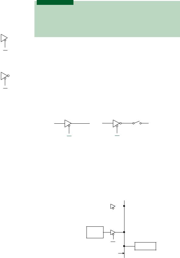
FIGURE 2.33
Tristate Buffers
FIGURE 2.34
Electrical Equivalent of Tristate
Operation
2.5 • Enable and Inhibit Properties of Logic Gates |
45 |
Tristate Buffers
K E Y T E R M S
Tristate buffer A gate having three possible output states: logic HIGH, logic LOW, and high-impedance.
High-impedance state The output state of a tristate buffer that is neither logic HIGH nor logic LOW, but is electrically equivalent to an open circuit.
Bus A common wire or parallel group of wires connecting multiple circuits.
In the previous section, logic gates were used to enable or inhibit signals in digital circuits. In the AND, NAND, NOR, and OR gates, however, the inhibit state was always logic HIGH or LOW. In some cases, it is desirable to have an output state that is neither HIGH nor LOW, but acts to electrically disconnect the gate output from the circuit. This third state is called the high-impedance state and is one of three available states in a class of devices known as tristate buffers.
Figure 2.33 shows the logic symbols for two tristate buffers, one with a noninverting output and one with an inverting output. The third input, OE (Output enable), is an activeLOW signal that enables or disables the buffer output.
When OE 0, as shown in Figure 2.34a, the noninverting buffer transfers the input value directly to the output as a logic HIGH or LOW. When OE 1, as in Figure 2.34b, the output is electrically disconnected from any circuit to which it is connected. (The open switch in Figure 2.34b does not literally exist. It is shown as a symbolic representation of the electrical disconnection of the output in the high-impedance state.)
IN |
OUT IN |
IN |
OUT HI-Z |
|
|||
|
OE 0 |
|
OE 1 |
|
a. Output enabled |
|
b. Output disabled |
This type of enable/disable function is particularly useful when digital data are transferred from more than one source to one or more destinations along a common wire (or bus), as shown in Figure 2.35. (This is the underlying principle in modern computer systems, where multiple components use the same bus to pass data back and forth.) The destination circuit in Figure 2.35 can receive data from source 1 or source 2. If the source circuits were directly connected to the bus, they could produce contradictory logic levels at the destination. To prevent this, only one source is enabled at a time, with control of this switching left to the two tristate buffers.
FIGURE 2.35 |
Digital |
|
|
|
|
Using Tristate Buffers to Switch |
|
||||
source 1 |
|
|
|
|
|
Two Sources to a Single |
|
|
|||
|
|
|
|
|
|
Destination |
|
|
|
|
|
|
OE1 |
||||
|
|
||||
Digital source 2
OE2
Destination
Bus

46C H A P T E R 2 • Logic Functions and Gates
2.6Integrated Circuit Logic Gates
K E Y T E R M S
Integrated circuit (IC) An electronic circuit having many components, such as transistors, diodes, resistors, and capacitors, in a single package.
Small scale integration (SSI) An integrated circuit having 12 or fewer gates in one package.
Medium scale integration (MSI) An integrated circuit having the equivalent of 12 to 100 gates in one package.
Large scale integration (LSI) An integrated circuit having from 100 to 10,000 equivalent gates.
Very large scale integration (VLSI) An integrated circuit having more than 10,000 equivalent gates.
Transistor-transistor logic (TTL) A family of digital logic devices whose basic element is the bipolar junction transistor.
Complementary metal-oxide-semiconductor (CMOS) A family of digital logic devices whose basic element is the metal-oxide-semiconductor field effect transistor (MOSFET).
Chip An integrated circuit. Specifically, a chip of silicon on which an integrated circuit is constructed.
Dual in-line package (DIP) A type of IC with two parallel rows of pins for the various circuit inputs and outputs.
Printed circuit board (PCB) A circuit board in which connections between components are made with lines of copper on the surfaces of the circuit board.
Breadboard A circuit board for wiring temporary circuits, usually used for prototypes or laboratory work.
Wire-wrap A circuit construction technique in which the connecting wires are wrapped around the posts of a special chip socket, usually used for prototyping or laboratory work.
Through-hole A means of mounting DIP ICs on a circuit board by inserting the
IC leads through holes in the board and soldering them in place.
Surface-mount technology (SMT) A system of mounting and soldering integrated circuits on the surface of a circuit board, as opposed to inserting their leads through holes on the board.
Small outline IC (SOIC) An IC package similar to a DIP, but smaller, which is designed for automatic placement and soldering on the surface of a circuit board. Also called gull-wing, for the shape of the package leads.
Thin shrink small outline package (TSSOP) A thinner version of an SOIC package.
Plastic leaded chip carrier (PLCC) A square IC package with leads on all four sides designed for surface mounting on a circuit board. Also called J-lead, for the profile shape of the package leads.
Quad flat pack (QFP) A square surface-mount IC package with gull-wing leads.
Ball grid array (BGA) A square surface-mount IC package with rows and columns of spherical leads underneath the package.
Data sheet A printed specification giving details of the pin configuration, electrical properties, and mechanical profile of an electronic device.
Data book A bound collection of data sheets. A digital logic data book usually contains data sheets for a specific logic family or families.
Portable document format (PDF) A format for storing published documents in compressed form.
2.6 • Integrated Circuit Logic Gates |
47 |
All the logic gates we have looked at so far are available in integrated circuit form. Most of these small scale integration (SSI) functions are available either in transistortransistor logic (TTL) or complementary metal-oxide-semiconductor (CMOS) technologies. TTL and CMOS devices differ not in their logic functions, but in their construction and electrical characteristics.
TTL and CMOS chips are designated by an industry-standard numbering system. TTL devices and the more recent members of the CMOS family are numbered according to the general format 74XXNN, where XX is a family identifier and NN identifies the specific logic function. For example, the number 74ALS00 represents a quadruple 2-input NAND device (indicated by 00) in the advanced low power Schottky (ALS) family of TTL. (Earlier versions of CMOS had a different set of unrelated numbers of the form 4NNNB or 4NNNUB where NNN was the logic function designator. The suffixes B and UB stand for buffered and unbuffered, respectively.)
Table 2.21 lists the quadruple 2-input NAND function as implemented in different logic families. These devices all have the same logic function, but different electrical characteristics.
Table 2.21 Part Numbers for a Quad 2-input NAND Gate in Different Logic Families
Part Number |
Logic Family |
|
|
74LS00 |
Low-power Schottky TTL |
74ALS00 |
Advanced low-power Schottky TTL |
74F00 |
FAST TTL |
74HC00 |
High-speed CMOS |
74HCT00 |
High-speed CMOS (TTL-compatible inputs) |
74LVX00 |
Low-voltage CMOS |
74ABT00 |
Advanced BiCMOS (TTL/CMOS hybrid) |
|
|
Table 2.22 lists several logic functions available in the high-speed CMOS family. These devices all have the same electrical characteristics, but different logic functions.
Table 2.22 Part Numbers for Different Functions within a Logic Family (High-Speed CMOS)
Part Number |
Function |
|
|
74HC00 |
Quadruple 2-input NAND |
74HC02 |
Quadruple 2-input NOR |
74HC04 |
Hex inverter |
74HC08 |
Quadruple 2-input AND |
74HC32 |
Quadruple 2-input OR |
74HC86 |
Quadruple 2-input XOR |
|
|
Until recently, the most common way to package logic gates has been in a plastic or ceramic dual in-line package, or DIP, which has two parallel rows of pins. The standard spacing between pins in one row is 0.1 (or 100 mil). For packages having fewer than 28 pins, the spacing between rows is 0.3 (or 300 mil). For larger packages, the rows are spaced by 0.6 (600 mil).
This type of package is designed to be inserted in a printed circuit board in one of two says: (a) the pins are inserted through holes in the circuit board and soldered in place; or (b) a socket is soldered to the circuit board and the IC is placed in the socket. The latter method is more expensive, but makes chip replacement much easier. A socket can occasionally cause its own problems by making a poor connection to the pins of the IC.
The DIP is also convenient for laboratory and prototype work, since it can also be inserted easily into a breadboard, a special type of temporary circuit board with internal connections between holes of a standard spacing. It is also convenient for wire-wrapping, a technique in which a special tool is used to wrap wires around posts on the underside of special sockets.
48 C H A P T E R 2 • Logic Functions and Gates
FIGURE 2.36
14-Pin DIP (Top View)
The outline of a 14-pin DIP is shown in Figure 2.36. There is a notch on one end to show the orientation of the pins. When the IC is oriented as shown and viewed from above, pin 1 is at the top left corner and the pins number counterclockwise from that point.
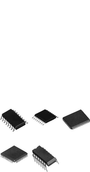
Besides DIP packages, there are numerous other types of packages for digital ICs, including, among others, small outline IC (SOIC), thin shrink small outline package (TSSOP), plastic leaded chip carrier (PLCC), quad flat pack (QFP), and ball grid array (BGA) packages. They are used mostly in applications where circuit board space is at a premium and in manufacturing processes relying on surface-mount technology (SMT). In fact, these devices represent the majority of IC packages found in new designs. Some of these IC packaging options are shown in Figure 2.37.
a. |
b. |
c. |
d. |
e. |
FIGURE 2.37
Some IC Packaging Options
SMT is a sophisticated technology which relies on automatic placement of chips and soldering of pins onto the surface of a circuit board, not through holes in the circuit board. This technique allows a manufacturer to mount components on both sides of a circuit board.
2.6 • Integrated Circuit Logic Gates |
49 |
Primarily due to the great reduction in board space requirements, most new ICs are available only in the newer surface-mount packages and are not being offered at all in the DIP package. However, we will look at DIP offerings in logic gates because they are inexpensive and easy to use with laboratory breadboards and therefore useful as a learning tool.
Logic gates come in packages containing several gates. Common groupings available in DIP packages are six 1-input gates, four 2-input gates, three 3-input gates, or two 4-in- put gates, although other arrangements are available. The usual way of stating the number of logic gates in a package is to use the numerical prefixes hex (6), quad or quadruple (4), triple (3), or dual (2).
Some common gate packages are listed in Table 2.23.
Table 2.23 Some Common Logic Gate ICs
Gate |
Family |
Function |
|
|
|
74HC00A |
High-speed CMOS |
Quad 2-input NAND |
74HC02 |
High-speed CMOS |
Quad 2-input NOR |
74ALS04 |
Advanced low-power Schottky TTL |
Hex inverter |
74LS11 |
Low-power Schottky TTL |
Triple 3-input AND |
74F20 |
FAST TTL |
Dual 4-input NAND |
74HC27 |
High-speed CMOS |
Triple 3-input NOR |
|
|
|
Information about pin configurations, electrical characteristics, and mechanical specifications of a part is available in a data sheet provided by the chip manufacturer. A collection of data sheets for a particular logic family is often bound together in a data book. More recently, device manufacturers have been making data sheets available on their corporate World Wide Web sites in portable document format (PDF), readable by a special program such as Adobe Acrobat Reader. Links to some of these manufacturers can be found on the Online Companion Web site for this book. (http://www.electronictech.com)
Figure 2.38 shows the internal diagrams of gates listed in Table 2.23. Notice that the gates can be oriented inside a chip in a number of ways. That is why it is important to confirm pin connections with a data sheet.
In addition to the gate inputs and outputs there are two more connections to be made on every chip: the power (VCC) and ground connections. In TTL, connect VCC to 5 Volts and GND to ground. In CMOS, connect the VCC pin to the supply voltage ( 3 V to 6 V) and GND to ground. The gates won’t work without these connections.
Every chip requires power and ground. This might seem obvious, but it’s surprising how often it is forgotten, especially by students who are new to digital electronics. Probably this is because most digital circuit diagrams don’t show the power connections, but assume that you know enough to make them.
The only place a chip gets its required power is through the VCC pin. Even if the power supply is connected to a logic input as a logic HIGH, you still need to connect it to the power supply pin.
Even more important is a good ground connection. A circuit with no power connection will not work at all. A circuit without a ground may appear to work, but it will often produce bizarre errors that are very difficult to detect and repair.
In later chapters, we will work primarily with complex ICs in PLCC packages. The power and ground connections are so important to these chips that they will not be left to chance; they are provided on a specially designed circuit board. Only input and output pins are accessible for connection by the user.
As digital designs become more complex, it is increasingly necessary to follow good practices in board layout and prototyping procedure to ensure even minimal functionality.