

20 |
1 Electromagnetic Field and Wave |
It can be seen that there is still a field outside the spherical shell of the conductor in this case. That is to say, the spherical shell cannot shield the field of the point charge.
Example 1.6 There is a grounded hollow metal sphere with an inner radius a and an outer radius b, with a point charge placed at the center of the sphere. Calculate the spatial potential distribution.
Solution This problem can be solved with the electrostatic field separation variable method. First, divide the space into three areas: area I (0 < rS < a), area II(a < rS < b), and area III(rS > b). The potentials in the three areas are Φ1(r), Φ2(r), Φ3(r), respectively, all of which satisfy the Laplace equation. The four boundary conditions are
rS a, Φ1(r) Φ2(r) 0 (Constant) |
|
|||||||
rS b, Φ2(r) Φ3(r) 0 (Constant) |
|
|||||||
|
rS → ∞, Φ3(r) → 0 |
|
||||||
rS → |
0, Φ1(r) → |
q |
|
|||||
|
|
|
||||||
4π ε0rS |
|
|||||||
Then, the solved spatial distribution of the potential is [1] |
|
|||||||
|
q |
a−b |
+ |
1 |
(0 < rS < a) |
|
||
4πε0 |
|
|
||||||
ab |
rS |
|
||||||
Φ(r) 0 |
|
|
|
(a < rS < b) (V ) |
(1.19) |
|||
0 |
|
|
|
(rS > b) |
|
|||
It can be seen that there is no field outside the spherical shell of the conductor in this case. That is to say, the grounded metal spherical shell can shield the field of the point charge.
1.3.2 Air Electric Wall
In this section, we will introduce the reflection characteristics of the semi-infinite ideal metal plane electromagnetic wave and explain that the electric wall is not necessarily composed of an ideal metal conductor, but “air” can also be used for shielding.
An ideal metal conductor is defined as a metal conductor with an infinite conductivity; a semi-infinite ideal metal plane, an ideal metal plane, is infinite.
The reflection of a semi-infinite ideal metal plane electromagnetic wave refers to an ideal conductor plane in which electromagnetic waves are obliquely incident from
1.3 The Reflection of Electromagnetic Wave |
21 |
a free space to a semi-infinite. There is no electromagnetic field in the ideal metal conductor, so it is only necessary to study the relationship between the reflected wave and the incident wave.
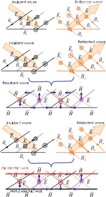
Suppose that the incident wave enters the interface between free space and a semiinfinite ideal metal plane at an angle of θi θ 0◦. We take the vertical polarization as an example for discussion. In this case, the incident wave is a linearly polarized wave that electric field is perpendicular to the incident surface, as shown in Fig. 1.7. Take z 0 as the interface and XOZ as the incident surface, because it is vertically
˜
polarized; Ei should be a complex vector in the y directions. Assume the electric
˜
field Er of the reflected wave is still in the y direction, according to electromagnetic
˜ ˜
field boundary conditions and electric fields E, magnetic field H, and glass pavilion
˜
vector S in plane electromagnetic waves are vertical to each other; we obtain that the
electromagnetic field of the synthetic wave in free space z < 0 is |
|
|||||||||||||
|
E˜ E˜ i |
+ E˜ r i y E˙ y |
|
|
|
|
(1.20) |
|||||||
H˜ H˜ i + H˜ r i x H˙ x + i z H˙ z |
|
(1.21) |
||||||||||||
where |
|
|
|
|
|
|
|
|
|
|
|
|
|
|
˙ y |
− |
|
˙ i0 |
|
|
z |
ze− jβx x |
|
|
|
|
|
||
E |
|
j2 E |
sin β |
|
(V/m) |
(1.22) |
||||||||
˙ x − |
˙ i0 |
cos θ |
cos |
|
z |
ze− jβx x /η |
0 |
(A/m) |
(1.23) |
|||||
H |
j2 E |
|
β |
|
|
|||||||||
˙ z − |
˙ i0 |
sin θ |
|
|
z |
ze− jβx x |
/η |
0 |
(A/m) |
(1.24) |
||||
H |
j2 E |
|
sin β |
|
|
|||||||||
From the expression of the synthetic wave, we see that the electric field of the synthetic wave is a linear polarization field in y direction; but the magnetic field is an elliptically polarized field on XOZ plane. In z direction, the synthetic electromagnetic field exhibits the properties of standing waves. The traveling wave in x direction forms a guided wave propagating along the metal surface. Detailed derivation of the synthesis wave and the characteristics of the guided wave can be found from reference [1].
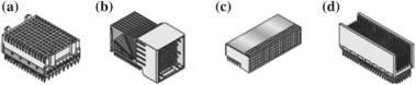
A typical application of the air electric wall technology is the AirMax VS connector, as shown in Fig. 1.8. The connector uses a virtual shield design with air as the high-efficiency dielectric, eliminating the need for staggered shielding, which significantly reduces the weight and price of the AC connector system. The connector achieves a rate of 2.5 GB/s and 6.25 GB/s and can be scaled to 12 GB/s high-speed computing and network system design.
22 |
1 Electromagnetic Field and Wave |
(a)
(b)
(c)
Fig. 1.7 Schematic diagram of the air electric wall: a schematic diagram of incident wave and reflected wave; b synthetic wave diagram; c metal electric wall and air electric wall
1.3 The Reflection of Electromagnetic Wave |
23 |
Fig. 1.8 Schematic diagram of the AirMax versus connectors
The formation of an air electric wall is the result of coherent electromagnetic waves in space. Using the coherence characteristics of electromagnetic waves is a useful technique for us to effectively control electromagnetic interference problems. For example, we can use the coherence characteristics of electromagnetic waves to find areas with weak synthetic fields and place susceptive devices and cables in these areas to reduce the mutual interference between devices.